Äîêóìåíòàöèÿ è îïèñàíèÿ www.docs.chipfind.ru
www.fairchildsemi.com
REV. 1.0 3/26/03
Features
· Multiple input formats
24 bit RGB
20 bit CCIR601
10 bit CCIR656
10 bit Digital Composite
· Synchronization modes
Master
Slave
Genlock
CCIR656
· Subcarrier modes
Free-run
Subcarrier reset
Genlock
DRS-lock
· Ancillary Data Control (ANC)
· Pixel rates from 10 MHz to 15 MHz
· Programmable horizontal timing
· Programmable vertical blanking interval (VBI)
· Line-by-line pedestal enable
· Programmable pedestal height from -20 IRE to 20 IRE
· Programmable burst amplitude and phase
· Controlled edge rates for
Sync
Burst
Active video
· Programmable color space matrix
· 8:8:8 video reconstruction
· Four 10 bit D/A's with independent trim
· Individual power down modes for each D/A
· Multiple output formats
RGB
Y P
B
P
R
Betacam
S-video
Composite
Digital composite output
· Pin-driven and data-driven, window keying
· Closed Caption waveform generation (13.5 MHz only)
· Sin(X)/X compensation filter
· 5 bit VBI line counter
· 3 bit field counter
· Internal test pattern generation
100% Color Bars
75% Color Bars
Modulated Ramp
Applications
· Broadcast Television
· Nonlinear Video Processing
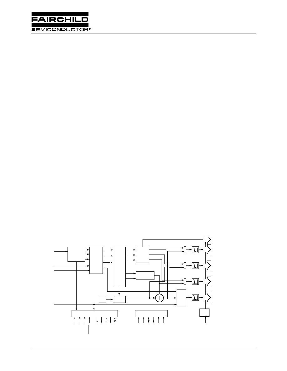
TMC2193
10 Bit Encoder
Block Diagram
PRE-
PROCESSOR
SYNC
INSERT
SYNC
INSERT
CC
KEY
MIX
sync/mid
Gr/Y
Y
Bl/Pb
Ch
Rd/Pr
Comp
PD[23:0]
OL[4:0]
CVBS[9:0]
COLOR
SPACE
MATRIX
KEY
FVHGEN
MPU
PXCK
HSIN
VSIN
DCVEN
HSOUT
VSOUT
LINE[4:0]
FLD[2:0]
PDCIN/PDCOUT
RESET
SERB
D[7:0]
A[1:0]/SA[1:0]
CS/SCL
R/W\/SD
A
VREF
CBYP4
CBYP3
CBYP2
CBYP1
DAC
REF.
U
V
Y
Gr/Y
Bl/Pb
Rd/Pr
OVERLAY
MIXER
REFDAC
DAC1
DAC2
DAC3
DAC4
RREF4
RREF3
RREF2
RREF1
CHROMA
PROCESSOR
65-6294-01
INTERP.
INTERP.
INTERP.
INTERP.
COMP2
gr/y
bl/cb
rd/cr

TMC2193
PRODUCT SPECIFICATION
2
REV. 1.0 3/26/03
Table of Contents
Features . . . . . . . . . . . . . . . . . . . . . . . . . . . .1
Applications. . . . . . . . . . . . . . . . . . . . . . . . .1
Block Diagram . . . . . . . . . . . . . . . . . . . . . . .1
10 Bit Encoder . . . . . . . . . . . . . . . . . . . . . . .1
LIst of Figures . . . . . . . . . . . . . . . . . . . . . . .3
LIst of Tables . . . . . . . . . . . . . . . . . . . . . . . .3
Pin Assignments . . . . . . . . . . . . . . . . . . . . .4
Pin Definitions . . . . . . . . . . . . . . . . . . . . . . .4
Functional Description . . . . . . . . . . . . . . . .7
Input Formats. . . . . . . . . . . . . . . . . . . . . . . . . . . 7
Gamma Correction . . . . . . . . . . . . . . . . . . . . . . 9
Color Space Matrix . . . . . . . . . . . . . . . . . . . . . . 9
Synchronization Modes . . . . . . . . . . . . . . . . . 12
Propagation Delay . . . . . . . . . . . . . . . . . . . . . . 12
Blanking Control . . . . . . . . . . . . . . . . . . . . . . . 13
Pixel Data Control . . . . . . . . . . . . . . . . . . . . . . 13
Edge Shaping. . . . . . . . . . . . . . . . . . . . . . . . . . 13
Horizontal Programming. . . . . . . . . . . . . . . . . 14
Vertical Timing . . . . . . . . . . . . . . . . . . . . . . . . . 17
Chrominance Processor . . . . . . . . . . . . . . . . . 23
Subcarrier Programming . . . . . . . . . . . . . . . 23
NTSC Subcarrier . . . . . . . . . . . . . . . . . 23
PAL Subcarrier . . . . . . . . . . . . . . . . . . . 23
PAL-M Subcarrier . . . . . . . . . . . . . . . . . 23
Subcarrier Synchronization . . . . . . . . . . . . . 24
SCH Phase Error Correction. . . . . . . . . . . . 24
Burst Envelope . . . . . . . . . . . . . . . . . . . . . . 25
Color-Difference Low-Pass Filters. . . . . . . . 25
Sync and Pedestal Insertion. . . . . . . . . . . . . . 25
Pedestal Enable . . . . . . . . . . . . . . . . . . . . . 25
Pedestal Height . . . . . . . . . . . . . . . . . . . . . . 26
Sync and Blank Insertion . . . . . . . . . . . . . . 26
Closed Caption Insertion . . . . . . . . . . . . . . . . 26
Line Selection . . . . . . . . . . . . . . . . . . . . . . . 26
Parity Generation . . . . . . . . . . . . . . . . . . . . 26
Operating Sequence . . . . . . . . . . . . . . . . . . 26
Interpolation Filters . . . . . . . . . . . . . . . . . . . . . 27
x/Sin(x) Filter . . . . . . . . . . . . . . . . . . . . . . . . . . 27
Output Data Formats . . . . . . . . . . . . . . . . . . . . 27
Digital Composite Output . . . . . . . . . . . . . . . . 28
Ancillary Data. . . . . . . . . . . . . . . . . . . . . . . . . . 28
Operating Modes. . . . . . . . . . . . . . . . . . . . . 29
Layering Engine. . . . . . . . . . . . . . . . . . . . . . . . 30
Overlay Mixer . . . . . . . . . . . . . . . . . . . . . . . 30
Hardware Keying . . . . . . . . . . . . . . . . . . . . . . . 31
Data Keying . . . . . . . . . . . . . . . . . . . . . . . . . . . 31
Parallel Microprocessor Interface . . . . . . . . . 31
Serial Control Port (R-Bus) . . . . . . . . . . . . . . . 33
Data Transfer via Serial Interface . . . . . . . . 33
Serial Interface Read/Write Examples . . . . 34
Control Register Map . . . . . . . . . . . . . . . . 35
Control Register Definitions . . . . . . . . . . 37
Absolute Maximum Ratings . . . . . . . . . . . 62
Operating Conditions . . . . . . . . . . . . . . . . 62
Electrical Characteristics . . . . . . . . . . . . . 64
Switching Characteristics . . . . . . . . . . . . 64
System Performance Characteristics . . . 65
Applications Discussion . . . . . . . . . . . . . 65
Layout Considerations . . . . . . . . . . . . . . . . . . 66
Output Low-Pass Filters . . . . . . . . . . . . . . . . . 69
Mechanical Dimensions . . . . . . . . . . . . . . 70
100-Lead MQFP . . . . . . . . . . . . . . . . . . . . . . . . 70
Ordering Information . . . . . . . . . . . . . . . . 72
Life Support Policy . . . . . . . . . . . . . . . . . . 72

PRODUCT SPECIFICATION
TMC2193
REV. 1.0 3/26/03
3
List of Figures
Figure 1.
Input Formats . . . . . . . . . . . . . . . . . . . . . .7
Figure 2.
24 bit Input Format . . . . . . . . . . . . . . . . . .7
Figure 3.
CCIR656 Input Format . . . . . . . . . . . . . . .8
Figure 4.
10 bit Input Format . . . . . . . . . . . . . . . . . .8
Figure 5.
20 bit 4:2:2 Input Format . . . . . . . . . . . . .8
Figure 6.
20 bit 4:4:4 Input Format . . . . . . . . . . . . .8
Figure 7.
Gamma Curves . . . . . . . . . . . . . . . . . . . .9
Figure 8.
Propagation Delay through the
Encoder . . . . . . . . . . . . . . . . . . . . . . . . .12
Figure 9.
Horizontal Timing . . . . . . . . . . . . . . . . . .15
Figure 10. Horizontal Timing Vertical Blanking . . .15
Figure 11. Horizontal Timing 1st Half-line. . . . . . .16
Figure 12. Horizontal Timing 2nd Half-line . . . . . .16
Figure 13. NTSC Vertical Interval . . . . . . . . . . . . . .17
Figure 14. PAL Vertical Interval . . . . . . . . . . . . . . . .19
Figure 15. PAL-M Vertical Interval . . . . . . . . . . . . . .21
Figure 16. Burst Envelope . . . . . . . . . . . . . . . . . . . .25
Figure 17. Gaussian Filter Response . . . . . . . . . . .25
Figure 18. Interpolation Filter. . . . . . . . . . . . . . . . . .27
Figure 19. Interpolation Filter Passband
Detail . . . . . . . . . . . . . . . . . . . . . . . . . . .27
Figure 20. X/SIN(X) Filter . . . . . . . . . . . . . . . . . . . .27
Figure 21. Layering Engine . . . . . . . . . . . . . . . . . . .30
Figure 22. Overlay Outputs . . . . . . . . . . . . . . . . . . .31
Figure 23. Data Keying . . . . . . . . . . . . . . . . . . . . . .31
Figure 24. Microprocessor Parallel Port
Write Timing . . . . . . . . . . . . . . . . . . . . . .32
Figure 25. Microprocessor Parallel Port
Read Timing . . . . . . . . . . . . . . . . . . . . . .32
Figure 26. Serial Port Read/Write Timing . . . . . . . .33
Figure 27. Serial Interface Typical Byte
Transfer. . . . . . . . . . . . . . . . . . . . . . . . . .34
Figure 28. Serial Interface Chip Address . . . . . . .34
Figure 29. Typical Analog Reconstruction Filter . . .65
Figure 30. Overall Response . . . . . . . . . . . . . . . . . .65
Figure 31. Typical Layout . . . . . . . . . . . . . . . . . . . . .67
Figure 32. ST-163E Layout . . . . . . . . . . . . . . . . . . .68
Figure 33. Pass Band . . . . . . . . . . . . . . . . . . . . . . .69
Figure 34. Stop Band. . . . . . . . . . . . . . . . . . . . . . . .69
Figure 35. 2T Pulse . . . . . . . . . . . . . . . . . . . . . . . . .69
Figure 36. Group Delay . . . . . . . . . . . . . . . . . . . . . .69
List of Tables
Table 1.
CSM Coefficient Range . . . . . . . . . . . . 10
Table 2.
Expected Output Values for the
CSM with YCBCR Inputs . . . . . . . . . . . 11
Table 3.
Expected Output Values for the
CSM with RGB Inputs. . . . . . . . . . . . . . 11
Table 4.
Coefficient sets YCBCR inputs . . . . . . . 11
Table 5.
Coefficient sets YCBCR inputs . . . . . . . 11
Table 6.
PDC Edge Control . . . . . . . . . . . . . . . . 13
Table 7.
Horizontal Line Equations. . . . . . . . . . . 14
Table 8.
Horizontal Timing Specifications. . . . . . 15
Table 9.
Vertical Interval Timing
Specifications . . . . . . . . . . . . . . . . . . . . 16
Table 10.
Default Horizontal Timing
Parameters . . . . . . . . . . . . . . . . . . . . . . 17
Table 11.
NTSC Field/Line Sequence and
Identification . . . . . . . . . . . . . . . . . . . . . 18
Table 12.
PAL Field/Line Sequence and
Identification . . . . . . . . . . . . . . . . . . . . . 20
Table 13.
PAL-M Field/Line Sequence and
Identification . . . . . . . . . . . . . . . . . . . . . 22
Table 14.
Standard Subcarrier Parameters . . . . . 24
Table 15.
Line by Line Pedestal Enable . . . . . . . . 25
Table 16.
Closed Caption Line Selection . . . . . . . 26
Table 17.
D/A Outputs . . . . . . . . . . . . . . . . . . . . . 27
Table 18.
Ancillary Data Format . . . . . . . . . . . . . . 28
Table 19.
Ancillary Data Control Phase . . . . . . 29
Table 20.
Ancillary Data Control Frequency. . . . . 29
Table 21.
Field Identification and Subcarrier
Reset Modes . . . . . . . . . . . . . . . . . . . . 29
Table 22.
Layering and Keying Modes . . . . . . . . . 30
Table 23.
Overlay Address Map . . . . . . . . . . . . . . 31
Table 24.
Parallel Port Control . . . . . . . . . . . . . . . 32
Table 25.
Serial Port Addresses. . . . . . . . . . . . . . 33
Table 26.
Control Register Map . . . . . . . . . . . . . . 35
TMC2193
PRODUCT SPECIFICATION
4
REV. 1.0 3/26/03
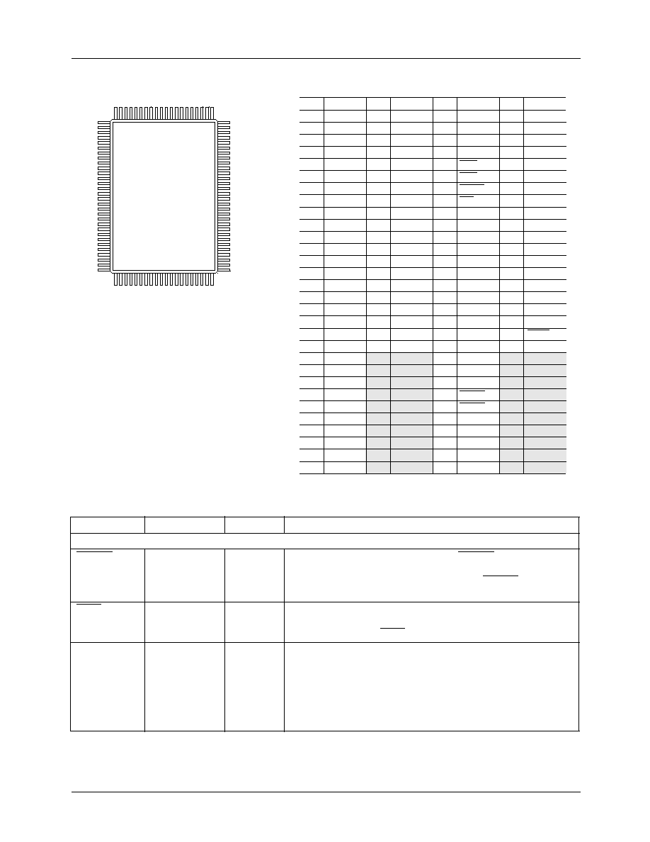
Pin Assignments
Pin Definitions
Pin Name
Pin Number
Value
Description
CLOCK, SYNC, & CONTROL INPUTS (6 pins)
DCVEN
57
TTL
Digital CVBS Output Enable. When DCVEN is LOW, the
Comp2 output prior to the D/A is routed to D7-0, FLD2-1
providing a digital composite output. When DCVEN is HIGH,
D7-0 and FLD2-1 operate in their normal mode.
HSIN
56
TTL
Horizontal Sync Input. When operating in slave, Genlock, or
DRS-Lock the TMC2193 will start a new horizontal line with
each falling edge of HSIN.
KEY
20
TTL
Hard Key selection. When the control register bit HKEN is set
HIGH and the hardware KEY pin is high, the video data
considered to be the foreground. is routed to the COMP2
output. This control signal is data aligned so that the pixel that is
present on the PD port when KEY signal is latched is at the
midpoint of the key transition. When HKEN is LOW, Key is
ignored.
1
30
31
50
65-6294-14
100
81
80
Pin
1
2
3
4
5
6
7
8
9
10
11
12
13
14
15
16
17
18
19
20
21
22
23
24
25
26
27
28
29
30
Function
VDDA
DAC4
CBYP4
AGND
DAC3
CBYP3
VDDA
RREF3
AGND
DAC2
CBYP2
VDDA
RREF2
AGND
DAC1
CBYP1
VDDA
RREF1
REFDAC
KEY
OL4
OL3
OL2
OL1
OL0
DGND
PD23
PD22
PD21
PD20
51
Pin
31
32
33
34
35
36
37
38
39
40
41
42
43
44
45
46
47
48
49
50
Function
PD19
PD18
PD17
PD16
PD15
PD14
PD13
PD12
VDD
DGND
PD11
PD10
PD9
PD8
PD7
PD6
PD5
PD4
PD3
PD2
Pin
51
52
53
54
55
56
57
58
59
60
61
62
63
64
65
66
67
68
69
70
71
72
73
74
75
76
77
78
79
80
Function
PD1
PD0
DGND
VDD
VSIN
HSIN
DCVEN
SER
CSVSCL
R/WVSDA
A1/SA1
A0/SA0
D7
D6
D5
D4
D3
D2
D1
D0
DGND
VDD
PDC
HSOUT
VSOUT
LINE4
LINE3
LINE2
LINE1
LINE0
Pin
81
82
83
84
85
86
87
88
89
90
91
92
93
94
95
96
97
98
99
100
Function
FLD2
FLD1
FLD0
CVBS9
CVBS8
CVBS7
CVBS6
CVBS5
CVBS4
CVBS3
CVBS2
CVBS1
CVBS0
RESET
PXCK
VDD
DGND
VREF
RREF4
AGND
PRODUCT SPECIFICATION
TMC2193
REV. 1.0 3/26/03
5
PXCK
95
TTL
Pixel Clock Input. PXCK is a clock signal that period is twice
the sample rate of the pixel data. The operating range is 20 to
30 MHz. The clock is internally divided by 2 to generate the
internal pixel clock, PCK. PXCK drives the entire TMC2193
except the asynchronous microprocessor interface.
RESET
94
TTL
Master Chip Reset. When LOW, All outputs are tri-stated and
the internal state machines and control registers are reset. At
rising edge of RESET, all outputs are active, the preset values
will be loaded into the control registers and the internal states
machines start to operate.
VSIN
55
TTL
Vertical Sync Input. When operating in slave, Genlock, or
DRS-Lock the TMC2193 will start a new vertical field with each
falling edge of VSIN that is coincident with HSIN.
SYNC & CONTROL OUTPUTS (11 pins)
FLD[2:0]
8183
TTL
Field Identifier. Field Identifier outputs the current field number.
For all video standards the field identifier will cycle through the
eight counts.
HSOUT
74
TTL
Horizontal Sync Output. The alignment of HSOUT to the pixel
data port or DCVBS port is controlled by control register
TSOUT.
LINE[4:0]
7680
TTL
Vertical Blanking Interval Line Identifier. LINE identifies the
current line number for the first 31 lines. If the line count is
greater than 31 then LINE is 11111b. The first line with a vertical
serration is considered to be line 0.
PDC
73
TTL
Pixel Data Control.
When PDCDIR = LOW: At a rising edge, The next pixel starts a
controlled ramp of the PD data. At a falling edge, the pixel prior
is the last PD used in the ramp. The rising edge is determined
by the PDCCNT control register, the falling edge of PDC is
determined by the horizontal timing registers.
When PDCDIR = HIGH: PDCIN is used to override the internal
PDC. When HIGH, the internal PDC controls the blank and
unblank window. When LOW, the video remains blanked
regardless of the internal PDC. All edges have the same ramp
control as the internal PDC.
VSOUT
75
TTL
Vertical Sync Output. The alignment of VSOUT to the pixel
data port or DCVBS port is controlled by control register
TSOUT.
DATA INPUTS (39 pins)
CVBS[9:0]
8493
TTL
Composite Data Input
OL[4:0]
2125
TTL
Overlay Control
PD[23:0]
2738, 4152
TTL
Component Data Input
ANALOG INTERFACE Video Out (5 pins)
Ref. DAC
19
0.675Vp-p
Selectable sync only or midpoint reference D/A
DAC1
15
1.35Vp-p
Composite or Green D/A
DAC2
10
1.35Vp-p
Luma or Blue D/A
DAC3
5
1.35Vp-p
Chroma or Red D/A
DAC4
2
1.35Vp-p
Composite D/A with optional keying
Pin Definitions
(continued)
Pin Name
Pin Number
Value
Description