
www.fairchildsemi.com
Features
∑ All-digital video encoding
∑ Internal digital oscillators, no crystals required
∑ Multiple input formats supported
≠ 24-bit and 15-bit GBR/RGB
≠ YC
B
C
R
422 or 444
≠ Color indexed
∑ 30 overlay colors (TMC22191)
∑ Fully programmable timing
∑ Supports input pixel rates of 10 to 15 Mpps
∑ 256 x 8 x 3 color look-up tables (bypassable on
TMC22191)
∑ 8-bit mask register
∑ 8-bit composite digital video input
∑ Hardware and 24-bit data keying
∑ Synchronizes with TMC22071 Genlocking Video
Digitizer
∑ 8:8:8 video reconstruction
∑ SMPTE 170M NTSC or CCIR Report 624 PAL
compatible
∑ Supports PAL-M and NTSC without pedestal
∑ Simultaneous S-VIDEO (Y/C) NTSC/PAL output
∑ 10-bit D/A conversion (three channels)
∑ Controlled edge rates
∑ 3 power-down modes
∑ Built-in color bars and modulated ramp test signals
∑ JTAG (IEEE Std 1149.1-1990) test interface
∑ Single +5V power supply
∑ 84 lead PLCC package
∑ 100 lead MQFP package
Description
The TMC22x91 digital video encoders convert digital com-
puter image or graphics data (in RGB, YCBCR, or color
indexed format) or a CCIR-601 signal into a standard analog
baseband television (NTSC or PAL) signal with a modulated
color subcarrier.
Both composite (single lead) and S-VIDEO (separate
chroma and luma) formats are active simultaneously at the
three analog output pins, each of which generates a standard
video-level signal into doubly-terminated 75
load.
The TMC22x91 accepts digitized video from the companion
TMC22071 Genlocking Video Digitizer. Soft switching
between video sources is done under either hardware or
programmable data control.
The TMC22191 offers 4-layer keying capability, bypassable
CLUT, and 30 Overlay colors.
The TMC22x91 is fabricated in a submicron CMOS process
and packaged in an 84 Lead Plastic Leadless Chip Carrier, or
in a 100 Lead Metric Quad Flat Pack. Performance is guar-
anteed from 0
∞
C to 70
∞
C.
Logic Symbol
PD23-0
24
PDC
CHROMA
LUNA
COMPOSITE
FRAME BUFFER
INTERFACE
GENLOCK
INTERFACE
MICROPROCESSOR
INTERFACE
VIDEO
OUTPUT
VHSYNC
VVSYNC
GHSYNC
GVSYNC
CS
R/W
KEY
TDI
TMS
TCK
JTAG TEST
INTERFACE
LDV
PXCK
CLOCKS
TDO
V
REF
COMP
R
REF
ANALOG
INTERFACE
BYPASS
RESET
27008A
TMC22x91
DIGITAL
VIDEO
ENCODER
CVBS7-0
8
D7-0
8
A1-0
2
OL4-0
6
BYPASS and OL4:0 on TMC22191 only.
TMC22091/TMC22191
Digital Video Encoders/Layering Engine
Rev. 1.1.0
TMC22091/TMC22191
PRODUCT SPECIFICATION
2
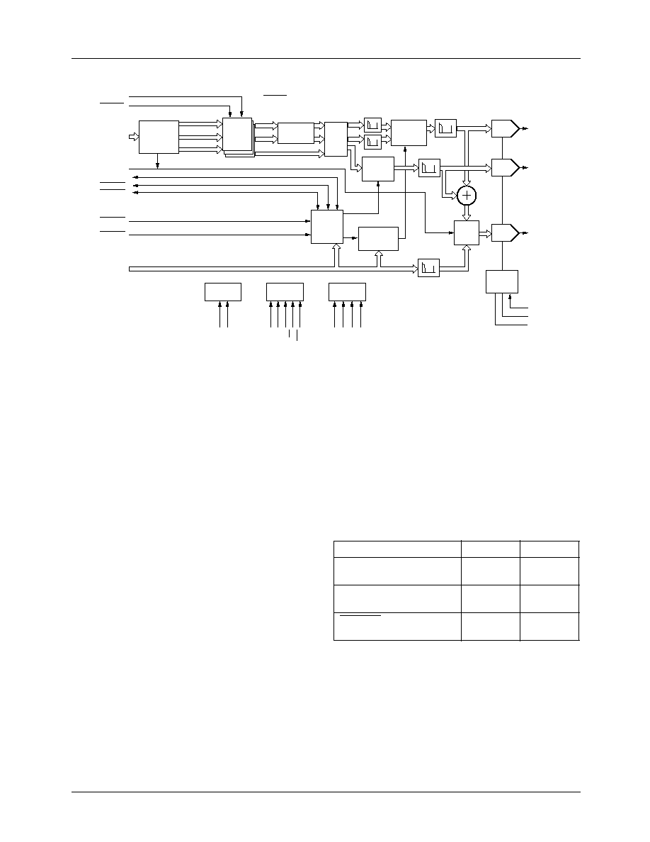
Block Diagram
OL4-0
PD23-0
CVBS7-0
BYPASS
KEY
PDC
VVSYNC
VHSYNC
G/R/Y MAP
R/R-Y
LPF
INT
10-bit
D/A
10-bit
D/A
10-bit
D/A
D/A
REF.
INT
CLOCK
CONTROL
JTAG
CLOCKS
MICROPROCESSOR
INTERFACE
FRAME BUFFER INTERFACE
GENLOCK
INTERFACE
ENCODED VIDEO OUTPUT
ANALOG
INTERFACE
JTAG TEST
INTERFACE
INT
DIGITAL
SYNC.
GEN.
INTERPOLATION
FILTERS
LPF
R-Y
CHROMA
LUMA
COMPOSITE
27006A
VREF
LDV
PXCK
RESET
D
7:0
A
1:0
CS
R/W
TDI
TMS
TCK
TDO
COMP
RREF
B-Y
B/B-Y
G/Y
B/G/CB
R/B/CR
Data Key
BYPASS and OL4:0 on TMC22191 only.
GHSYNC
GVSYNC
256 x 8 x 3
COLOR
LOOK-UP
TABLE
FORMATTER
MASK, KEY
COMPARATOR
MATRIX
CHROMA
MODULATOR
SYNC,
BLANK
INSERT
VIDEO
SWITCH
SUBCARRIER
SYNTHESIZER
INTER-
POLATOR
4:2:2/4:4:4
Functional Description
The TMC22091 and TMC22191 are totally integrated, fully-
programmable digital video encoders with simultaneous
composite and Y/C (S-VIDEO) outputs. The TMC22x91
video outputs are compatible with SMPTE 170M NTSC,
CCIR Report 624 PAL, PAL-M, and NTSC without pedestal
television standards. No external component selection or
tuning is required.
The encoders accept digital image data at the PD port in one
of several formats, which are matrixed into luminance and
chrominance components. The chrominance signals are
modulated onto a digitally synthesized subcarrier. The lumi-
nance and chrominance signals are separately interpolated to
twice the pixel rate, and converted to analog levels by 10-bit
D/A converters. They are also digitally combined and the
resulting composite signal is output by a third 10-bit D/A
converter. This composite signal may be keyed (pixel rate
switching) with a second composite digital video signal pre-
sented to the encoder.
The output video frames may be internally timed by the
TMC22x91, synchronized with the external frame buffer, or
slaved to the companion Genlocking Video Digitizer
(TMC22071). All operational parameters are fully program-
mable over a standard microprocessor port.
Table 1 shows the key features that distinguish between the
TMC22091 and TMC22191. All of the information pre-
sented in this data sheet applies to both products unless oth-
erwise noted. Statements, paragraphs, tables, and figures that
apply to only one or two of the encoders have notation speci-
fying the applicable part number.
Timing
The encoder operates from a single clock at twice the system
pixel rate. This frequency may be set between 20 MHz and
36 MHz (pixel rates of 10 Mpps to 18 Mpps). Within this
range are included CCIR-601, D2, and square-pixel formats,
as well as a variety of computer-specific pixel rates. An array
of programmable timing registers allows the software selec-
tion of all pertinent signal parameters to produce NTSC
(with or without 7.5 IRE pedestal) and PAL, and PAL-M
outputs.
Table 1. Comparing the TMC22x91 Encoders
Input Formatting
The input section accepts a variety of video and graphics for-
mats, including 24-bit GBR and RGB, 15-bit GBR and
RGB, YCBCR422, YCBCR444, and 8-bit color-indexed data
(Figure 1a and 1b).
The input section of the TMC22x91 includes a key compara-
tor which monitors the pixel data port with three independent
8-bit comparators, and invokes a video key when the selected
registers match the incoming data.
Feature
TMC22091 TMC22191
OL
4-0
pixel inputs for 30
overlay colors
No
Yes
Number of video layers
supported
2
4
BYPASS input for
bypassing CLUTs
No
Yes

PRODUCT SPECIFICATION
TMC22091/TMC22191
3
Mask Register
A Mask Register is provided which is logically ANDed with
incoming color-index data to facilitate pixel animation and
other special graphics effects. The Mask Register is ahead of
the Data Key comparators and is enabled only when color-
index input is selected. Mask Register programming and
operation are similar to that of the 171/176 family of graph-
ics RAMDACS.
Color Lookup Table
The Color Lookup Table (CLUT) is a 256 x 8 x 3 random-
access memory. It provides means for offset, gain, gamma,
and color correction in RGB and YC
B
C
R
operating modes. It
provides a full 24-bit color lookup function for color-index
mode. It can be loaded in the same manner as a standard
VGA RAMDAC.
Colorspace Conversion Matrix and
Interpolator
The matrix converts RGB data (whether from RGB inputs or
color-indexed CLUT data) into Y, B-Y, R-Y format for
encoding. In input configurations where the pixel input is
already in Y, B-Y, R-Y format, the matrix is bypassed. When
pixel data is input in YC
B
C
R
422 format, the interpolation fil-
ters produce YC
B
C
R
444 for encoding.
Sync Generator
The TMC22x91 can operate in Master, Genlock, or Slave
modes. In Master and Genlock modes, the encoder internally
generates all timing and sync signals, and provides Horizon-
tal Sync, Vertical Sync, and Pixel Data Control (PDC) to the
external frame buffer circuitry. PDC is independently select-
able to function as an input or an output. In Genlock mode,
the TMC22x91 timing is controlled by the TMC22071 Gen-
locking Video Digitizer over the CVBS
7-0
bus, GVSYNC,
and GHSYNC. The encoder, in turn, produces VHSYNC,
VVSYNC, and PDC for the frame buffer interface.
Figure 1a. Pixel Data Format
MSB
23
LSB
0
16
GBR444
MODE
24300A
RGB444
YCBCR444
YCBCR422
COLOR INDEX
GBR15
RGB15
00011000
Format Control Register
00010000
00011100
00011101
0001X011
00011010
00010010
G
B
R
R
G
B
Y
C
B
C
R
G
B
R
R
G
B
Y
C
B/
C
R
Pixel
15
G
7
G
0
B7
B
0
R
7
R
0
R
7
R
0
G
7
G
0
B
7
B
0
Y
7
Y
0
C
B7
C
B0
R
R7
R
R0
Y
7
Y
0
C
B7
C
R7
C
B0
C
R0
P
7
P
0
G
4
R
0
R
4
G
0
R
0
B
4
G
4
B
0
G
0
R
4
B
4
B
0
8
7
MSB
LSB

TMC22091/TMC22191
PRODUCT SPECIFICATION
4
In Slave mode, VHSYNC, VVSYNC, and PDC (optional)
are inputs to the TMC22x91. These inputs determine when
new lines, frames, and active picture areas begin. The exter-
nal controlling circuitry needs to establish the correct timing
for these signals.
Horizontal and vertical synchronization signals are digitally
generated by the TMC22x91 with controlled rise and fall
times on all sync edges, the beginning and end of active
video, and the burst envelope. All elements of horizontal
sync timing are programmable, as are the frequency, phase,
and duration of color burst.
Video Input
The TMC22x91 accepts genlocked synchronization data and
digital composite video signals from the TMC22071 Gen-
locking Video Digitizer over the 8-bit CVBS bus. The
encoder synchronizes its digital subcarrier oscillator to the
video input from the TMC22071 with this data. The compos-
ite video data output from the TMC22071 is passed to the
internal video switch for keying with the encoded pixel data.
Chroma Modulator
A 32-bit digital subcarrier synthesizer feeds a quadrature
modulator, producing a digital chrominance signal. The rela-
tive phases of the burst and active video portions of the sub-
carrier can be individually adjusted to compensate for
external phase errors and to effect a hue control.
Interpolation Filters
Interpolation filters on the luminance and chrominance sig-
nals double the pixel rate in preparation for D/A conversion.
This band-limited process greatly simplifies the output filter-
ing required following the D/A converters and dramatically
reduces sin(x)/x distortion.
An interpolation filter on the CVBS data similarly raises the
sample rate of the video signal, for mixing with the encoded
pixel data.
Composite Video Switch
The Composite Video Switch selects between the composite
video input (CVBS) and the composite encoded pixel data
on a pixel-by-pixel basis, under the control of a key function.
Keying may be managed by hardware or software. The hard-
ware key input (KEY pin) directly controls the video switch.
The encoder may be programmed to operate with a data key,
represented by three 8-bit registers that compare with the 24
input bits. They operate in all input modes and may be indi-
vidually enabled or disabled.
D/A Converters
The analog outputs of the TMC22x91 are the outputs of
three 10-bit D/A converters, operating at twice the pixel
clock rate. The outputs are capable of driving standard video
levels into a doubly-terminated 75
coaxial video cable
(37.5
total load). An internal voltage reference is provided
which can be used to provide reference current for the three
D/A converters. For accurate video levels, an external fixed
or variable voltage reference source is recommended. The
video signal levels from the TMC22x91 may be adjusted to
overcome the insertion loss of analog low-pass output filters.
The D/A converters on the TMC22x91 may be powered-
down via Control Register 0E bits 5 and 6. The
COMPOSITE D/A is controlled by bit 6 and the LUMA and
CHROMA D/A converters are controlled by bit 5.
Figure 1b. Pixel Data Format (TMC22191 when CLUTs are Bypassed)
MSB
23
LSB
0
16
GBR444
MODE
RGB444
YCBCR444
YCBCR422
COLOR INDEX
*C
B
and C
R
are loaded on alternate LDV cycles
RGB15
GBR15
24393A
01011000
Format Control Register
01010000
0101X000
0101X001
0101X011
01010010
01011010
G
B
R
R
G
B
Y
C
B
C
R
R
G
B
Y
C
B*
C
R*
Pixel
15
G
7
G
0
B7
B
0
R
7
R
0
R
7
R
0
G
7
G
0
B
7
B
0
Y
7
Y
0
C
B7
C
B0
C
R7
C
R0
Y
7
Y
0
C
B7
C
B0
C
R7
C
R0
P
7
P
0
Pixel
P
7
P
0
Pixel
P
7
P
0
R
4
B
0
R
0
G
4
G
0
B
4
8
7
MSB
LSB
G
B
R
G
4
R
0
G
0
B
4
B
0
R
4

PRODUCT SPECIFICATION
TMC22091/TMC22191
5
Microprocessor Interface
The microprocessor interface employs a 13 line format. The
RESET pin sets all internal state machines to their initialized
conditions, disables the analog outputs, sets the internal
SRESET bit LOW (reset condition), and places the encoder
in a power-down mode. All register and CLUT data are
maintained in power-down mode. If the HRESET bit is set
HIGH, line 1 field 1 is started when RESET goes HIGH, and
SRESET is ignored. If HRESET is LOW, the encoder
remains idle after RESET goes HIGH until Control Register
bit SRESET is set HIGH, which initiates line 1 field 1.
Two address lines are provided and decoded for access to the
internal Control Registers and CLUT. Control Registers and
CLUT are accessed by loading a desired address through the
8-bit D
7-0
port, followed by the desired data read or write for
that address. Both the CLUT and the Control Registers are
self-indexing, allowing continuous reads or writes to succes-
sive addresses.
JTAG Test Interface
The TMC22x91 includes a standard 4-line JTAG (IEEE Std
1149.1-1990) test interface port, providing access to all digi-
tal input/output data pins. This is provided to facilitate com-
ponent and board-level testing.
Test/Validation Mode
The TMC22x91 may be configured to produce standard
color bars or a 40 IRE modulated (or unmodulated) video
ramp, independent of any pixel or video data input. Color
bars are useful as an idle system output signal. The test sig-
nals may be used to verify proper operation of the analog
video signal chain.
TMC22090/TMC22190 Compatibility
The TMC22090 and TMC22190 are earlier versions of the
TMC22091 and TMC22191, respectively. They lack the fol-
lowing features of the newer versions:
1.
Selectable Setup (to support NTSC EIA-J video output
for Japan)
2.
PAL-M format (for South American applications)
3.
Extended EH and SL intervals (to support pixel rates
above 15 Mpps)
4.
Individual D/A power-down (to reduce total dissipation
when some outputs are not required)
5.
Luminance I/O processing (to reduce flicker in graphics
applications)
These features are controlled by registers 0E and 0F, and
enabled by setting Register OE bit 7 to ONE. If an applica-
tion of the TMC22x90 is programmed with this bit set to
ZERO (as recommended in the product documentation) then
the corresponding TMC22x91 will perform identically.
Though the earlier parts continue to be available, it is recom-
mended that the newer devices be used in new designs for
the additional flexibility. Older designs may be readily
converted to the newer versions to take advantage of the
added features and lower cost of the later technology.