www.fairchildsemi.com
REV. 1.0.0 2/4/03
Features
∑ Very high performance, low cost
∑ Adaptive comb-based decoding
∑ Multiple pin-compatible versions
- 3-line, 2-line, and band-split
- 8- and 10-bit processing
∑ Internal digital linestores
∑ Supports NTSC/PAL field and NTSC frame based
decoding
∑ Multiple input formats
- CCIR-601/624 (D1), D2, CVBS, YC
∑ Multiple output formats
- CCIR-601/624 (D1), RGB, YC
B
C
R
∑ 10-18 Mpps data rate
∑ Parallel and serial control interface
∑ Single +5V power supply
Applications
∑ Studio television equipment
∑ Personal computer video input
∑ MPEG and JPEG compression inputs
Description
The TMC22x5yA family of Digital Video Decoders offers
unprecedented, broadcast-quality video processing perfor-
mance in a single chip. It accepts line-locked or subcarrier-
locked composite, YC, or D1 digital video and produces dig-
ital components in a variety of formats.
An internal three-line adaptive comb decoder structure pro-
duces optimal picture quality with a wide range of source
material. NTSC/PAL field and NTSC frame based decoding
is supported with external memory. Full comb programma-
bility allows the user to tailor the decoder's response to a
particular systems goals.
A family of products offers 3-line, 2-line, and simple decod-
ers in 8-bit and 10-bit versions--all in a pin and software-
compatible format. Serial and parallel control ports are pro-
vided. These submicron CMOS devices are packaged in a
100-lead Metric Quad Flat Pack (MQFP).
Related Products
∑ TMC22071 Genlocking Video Digitizer
∑ TMC22x9x 8 bit Digital Video Encoders
∑ TMC2081 Digital Video Mixer
∑ TMC3003 Triple 10-bit D/A Converter
∑ TMC1185 10 bit A/D converter
∑ TMC2192 10 bit video encoder
∑ TMC2072 Enhanced Genlocking Video Digitizer
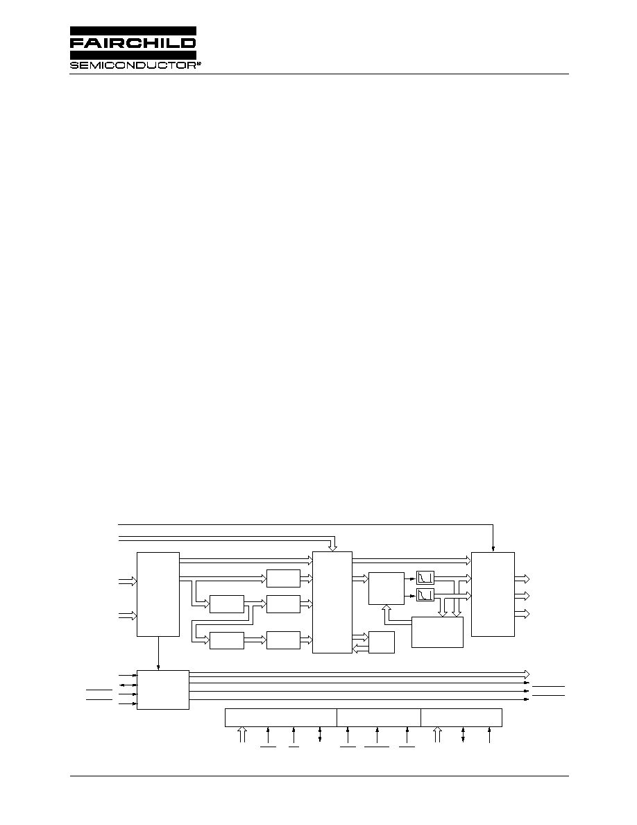
Block Diagram
65-22x5y-01
Input
Processor
Output
Processor
Adaptive
Comb
Filter
VIDEOA
9-0
VIDEOB
9-0
G/Y
9-0
MASTER
1-0
BUFFER
CLOCK
HSYNC
VSYNC
LDV
DHSYNC
DVSYNC
DREF
FID
2-0
B/Cb
9-0
R/Cr
9-0
SER
A1-0
SA
2-0
RESET
SET
R/W
SDA
CS
SCL
D 7-0
Parallel Control
Serial Control
Global Control
Internal
Sync Pulse
Generator
Y/C Split0
Y/C Split1
Linestore1
Linestore2
Y/C Split2
Chroma
Demod
Comb
Fail
Burst
Locked
Loop
TMC22x5yA
Multistandard Digital Video Decoder
Three-Line Adaptive Comb Decoder Family, 8 & 10 bit

TMC22x5yA
PRODUCT SPECIFICATION
2
REV. 1.0.0 2/4/03
Table of Contents
Features ......................................................................1
Applications ...............................................................1
Description .................................................................1
Block Diagram ............................................................1
Contents .....................................................................2
List of Tables and Figures ........................................3
General Description ...................................................4
Input Processor...............................................................4
Adaptive Comb Filter.....................................................4
Output Processor ............................................................5
Parallel and Serial Microprocessor Interfaces................5
Pin Assignments ........................................................5
Pin Descriptions.........................................................6
Control Register Map.................................................8
Control Register Definitions ...................................11
Decoder Introduction...............................................40
YC Separation ..............................................................40
Comb Filter Architecture for YC Separation ...............41
YC Line-Based Comb Filters.......................................42
D1 Line-Based Comb Filters .......................................42
NTSC Frame and Field Based Decoders ...............42
Composite Frame-Based Comb Filters ........................42
Composite Field-Based Comb Filters ..........................42
PAL Field Comb Decoders ......................................42
Composite PAL Field Comb Filters.............................42
The TMC22x5yA Comb Filter Architecture ............43
TMC22x5yA Functional Description.......................44
Input Processor.............................................................44
Bandsplit Filter (BSF) ..................................................44
Comb Filter Input.........................................................45
Adaptive Comb Filter...................................................47
Comb Fails................................................................49
Comb Fail Detection ....................................................49
Generation of the Comb Fail Signals .....................50
Luma Error Signals ......................................................50
Hue and Saturation Error Signals.................................50
Picture Correlation .......................................................50
Adapting the Comb Filter ............................................50
XLUT ...........................................................................51
Digital Burst Locked Loop ..........................................53
Color Kill Counter .......................................................53
PAL Color Frame Bit ...................................................55
Hue Control..................................................................55
System Monitoring of the Burst Loop Error ................55
Clamp Circuit .............................................................. 55
Pedestal Removal ........................................................ 55
Clamp Generator ......................................................... 55
Luma Notch Filter ....................................................... 56
Matrix .......................................................................... 56
Programmable U Scalar............................................... 56
Programmable V Scalar............................................... 56
Programmable Y Scalar............................................... 56
Programmable MS Scalar............................................ 56
Fixed (B-Y) and (R-Y) Scalars ................................... 56
Y Offset ....................................................................... 57
Matrix Limiters............................................................ 57
Examples of Output Matrix Operation ........................ 57
Simple Luma Color Correction ................................... 58
C
B
C
R
MSB Inversion ................................................. 58
Output Rounding ......................................................... 58
Output Formats............................................................ 58
Decimating C
B
C
R
Data............................................... 58
Multiplexed YC
B
C
R
Output (TRS Words Inserted)... 58
YC Outputs.................................................................. 58
The LDV Clock ........................................................... 58
Sync Pulse Generator ............................................. 59
Internal Field and Line Numbering Scheme ............... 59
Timing Parameters .................................................. 61
Subcarrier Programming ............................................. 61
Horizontal Timing ....................................................... 61
Horizontal and Vertical Timing Parameters................ 61
Vertical Blanking ........................................................ 62
VINDO Operation ....................................................... 65
Video Measurement ................................................. 65
Pixel Grab.................................................................... 65
Composite Line Grab .................................................. 67
Parallel Microprocessor Interface ............................... 67
Serial Control Port (R-Bus) ......................................... 68
Equivalent Circuits and Threshold Levels ............ 71
Absolute Maximum Ratings.................................... 72
Operating Conditions .............................................. 73
Electrical Characteristics ........................................ 75
Switching Characteristics ....................................... 76
System Performance Characteristics .................... 76
Programming Examples.......................................... 77
Programming Worksheet ........................................ 81
Related Products ..................................................... 82
Ordering Information ............................................... 84

PRODUCT SPECIFICATION
TMC22x5yA
REV. 1.0.0 2/4/03
3
List of Tables and Figures
Table 1.
TMC22x5yA Decoder Family ................. 4
Table 2.
Normalized Subcarrier Frequency
as a Function of Pixel Data Rates....... 45
Table 3.
Comb Filter Architecture ..................... 48
Table 4.
Simple Example of an Adaptive
Comb Filter Architecture ..................... 48
Table 5.
Adaption Modes ................................... 51
Table 6.
XLUT Input Selection ........................... 52
Table 7.
XLUT Output Function ......................... 52
Table 8.
XLUT Special Function Definitions..... 52
Table 9.
PAL-B,G,H,I Bruch
Blanking Sequence .............................. 53
Table 10. PAL-M Bruch Blanking Sequence ...... 54
Table 11. Blanking Level Selection ..................... 55
Table 12. Adaptive Notch Threshold Control..... 55
Table 13. Matrix Limiters...................................... 57
Table 14. Output Format ...................................... 58
Table 15. NTSC Field and Line Numbering ........ 59
Table 16. PAL B,G,H,I Field and
Line Numbering .................................... 59
Table 17. PAL M Field and Line Numbering ....... 59
Table 18. Vertical Blanking Period ...................... 60
Table 19. Vertical Burst Blanking Period............ 60
Table 20. Table of Line Idents, LID[4:0] .............. 60
Table 21. Timing Offsets ...................................... 61
Table 22. PAL VINDO operation .......................... 63
Table 23. Pixel Grab Control................................ 66
Table 24. Parallel Port Control............................. 67
Table 25. Serial Port Addresses .......................... 69
Figure 1.
Logic Symbol.......................................... 4
Figure 2.
Pixel Data Format ................................... 4
Figure 3.
Fundamental Decoder
Block Diagram ...................................... 40
Figure 4.
Comparison of the Frequency
Spectrum of NTSC and PAL
Composite Video Signals .................... 40
Figure 5.
Examples of Notch and Bandpass
Filters..................................................... 41
Figure 6.
............................................................... 41
Figure 7.
Chrominance Vector Rotation in
PAL and NTSC ...................................... 42
Figure 8.
Chrominance Vector Rotation Over
4 Fields in NTSC ................................... 42
Figure 9.
Chrominance Vector Rotation Over
4 Fields in PAL...................................... 42
Figure 10. TMC22x5yA Line Based Comb
Filter Architecture ................................ 43
Figure 11. Input Processor .................................... 44
Figure 12. Complementary Bandsplit Filter ......... 44
Figure 13. Bandsplit Filter, Full Frequency
Response .............................................. 45
Figure 14. Bandsplit Filter, Passband
Response .............................................. 45
Figure 15. Block Diagram of Comb Filter Input ... 46
Figure 16. Signal Flow Around the Adaptive
Comb Filter ........................................... 47
Figure 17. Example of a Comb Fail Using a NTSC
Two Line Comb Filter........................... 49
Figure 18. Generation of Upper and Lower Comb
Fail Signals ........................................... 50
Figure 19. Comb Filter Selection .......................... 51
Figure 20. XLUT Input Selection ........................... 52
Figure 21. Block Diagram of Digital Burst
Locked Loop ......................................... 53
Figure 22. Gaussian Low Pass Filters.................. 54
Figure 23. Gaussian LPF Passband Detail........... 54
Figure 24. Output Processor Block Diagram....... 55
Figure 25. Adaptive Notch Filters ......................... 56
Figure 26. Luminance Notch Filter ....................... 56
Figure 27. Horizontal Timing ................................. 61
Figure 28. External HSYNC and VSYNC Timing
for Field 1(3, 5, or 7) ............................. 62
Figure 29. NTSC Vertical Interval.......................... 62
Figure 30. PAL-B,G,H,I,N Vertical Interval............ 62
Figure 31. PAL-M Vertical Interval ........................ 63
Figure 32. Pixel Grab Locations............................ 64
Figure 33. Relationship Between Pixel Count
and Pixel Grab Value............................ 65
Figure 34. Microprocessor Parallel Port ≠
Write Timing.......................................... 66
Figure 35. Microprocessor Parallel Port ≠
Read Timing.......................................... 68
Figure 36. Serial Port Read/Write Timing............. 69
Figure 37. Serial Interface ≠
Typical Byte Transfer........................... 70
Figure 38. Equivalent Digital Input Circuit ........... 71
Figure 39. Equivalent Digital Output .................... 71
Figure 40. Threshold Levels for Three-state........ 71
Figure 41. Input Timing Parameters ..................... 72
Figure 42. Functional Block Diagram of the
TMC22x5yA G/Y, B/U, and R/V Output
Stage...................................................... 73
Figure 43. Output Timing Parameters .................. 74

TMC22x5yA
PRODUCT SPECIFICATION
4
REV. 1.0.0 2/4/03
General Description
The TMC22x5yA digital decoder can be used as a universal
input to digital video processing systems by decoding digital
composite video and transcoding digital component inputs
into a common data format.
The digital comb filter decoder implements one of sixteen
comb filter architectures to produce luminance and color dif-
ference component signals which are virtually free of the
cross-color and cross-luminance artifacts associated with
simple bandsplit filter decoders.
Table 1. TMC22x5yA Decoder Family
Because the cost/performance tradeoff varies among applica-
tions, the TMC22x5yA decoder has been developed as a
family of six parts. They are all assembled in the same
package, and fit the same footprint. The register maps are
identical.
Figure 1. Logic Symbol
The devices come in 8- and 10-bit resolution versions (see
Figure 2 for data alignment between 8- and 10-bit versions).
Within each resolution version there are three models, offer-
ing three-line adaptive comb filtering, two-line adaptive
comb filtering, and simple decoding. The TMC22153A
10-bit three-line comb filter can be programmed to emulate
any of the other parts. All prototyping can be performed with
this version to evaluate performance tradeoffs, and lower-
cost versions are easily substituted in production.
Input Processor
The digitized video and clocks provided to the decoder can
be either locked to the line frequency or the subcarrier fre-
quency of the digitized waveform, providing broadcast qual-
ity decoding from the NTSC square pixel rate of 12.27 MHz
to the PAL four times subcarrier pixel rate of 17.73 MHz.
Figure 2. Pixel Data Format
Inputs containing embedded GRS (Fairchild Video Input
Processors), TRS words (D1 multiplexed component sig-
nals), and TRS-ID words (deserialized D2 signals) can be
used to lock the internal horizontal and vertical state
machines to the embedded information. If this information is
not provided, external horizontal and vertical syncs are
required for all line-locked input formats, and are optional
for NTSC inputs locked to four times the subcarrier (4*Fsc).
A simple sync separator is provided for digitized inputs
locked to the subcarrier frequency: the internal sync separa-
tor locks to the mid point of syncs during the vertical field
group, then flywheels during the active portion of the field.
For this reason, the DHSYNC and DVSYNC operations are
not guaranteed in subcarrier mode.
Adaptive Comb Filter
The line based adaptive comb filter in the TMC22x5yA adds
or subtracts the high frequency data from three adjacent field
lines to produce the average of the high frequency luminance
by canceling the chrominance signals, which in flat fields of
color are 180 degrees apart. Unfortunately flat fields of color
are rare and, when vertical transitions in the picture occur,
the output of the comb filter contains a mixture of both high
frequency luminance and chrominance, at which time the
comb fails. To avoid the comb filter artifacts that occur when
this happens, three sets of error signals are sent to a user-pro-
grammable lookup table, allowing the output of the comb fil-
ter to be mixed with the output of an internal bandsplit
decoder.
To produce these comb fail error signals, the video on each
of the inputs to the comb filter is passed through a simple
bandsplit decoder. The low-frequency portion of the signal is
TMC2215yA
TMC2205yA
Function
3
2
1
3
2
1
10-bit Data
8-bit Data
D1 Interface
Line-Locked Mode
f
SC
-Locked Mode
Genlock Mode
NTSC Frame Comb
NTSC/PAL Field Comb
3-Line Comb
2-Line Comb
Line Grab
Pixel Grab
65-22x5yA-02
VIDEOA
9-0
BUFFER
LDV
HSYNC
MASTER
TMC22x5yA
Multistandard
Digital
Video
Decoder
CLOCK
CS
VSYNC
R/W
D
7-0
A
1-0
VIDEOB
9-0
G/Y
9-0
B/C
B9-0
R/C
R9-0
FID
2-0
AVOUT
DHSYNC
DVSYNC
SER
SET
RESET
SA
2-0
SDA
SCL
MSB
LSB
VA
9
VB
9
G/Y
9
B/C
B9
R/C
R9
VA
8
VB
8
G/Y
8
B/C
B 8
R/C
R8
∑∑∑
VA
2
VB
2
G/Y
2
B/C
B2
R/C
R2
VA
1
VB
1
G/Y
1
B/C
B1
R/C
R1
VA
0
VB
0
G/Y
0
B/C
B0
R/C
R0
10 bit
VA
9
VB
9
G/Y
9
B/C
B9
R/C
R9
VA
8
VB
8
G/Y
8
B/C
B 8
R/C
R8
∑∑∑
VA
2
VB
2
G/Y
2
B/C
B2
R/C
R2
N/C
N/C
N/C
N/C
N/C
N/C
N/C
N/C
N/C
N/C
8 bit
PRODUCT SPECIFICATION
TMC22x5yA
REV. 1.0.0 2/4/03
5
assumed to be luminance and the high frequency portion is
processed as chrominance to find the magnitude and phase of
the chrominance vector. These three components are then
compared across the (0H & 1H) and (1H & 2H) taps of the
comb filter to produce the difference in luminance, chromi-
nance magnitude, and chrominance phase. These differences
are then translated in the user-programmable lookup table to
produce the "K" signal which controls the complementary
mix between the output of the comb filter and the simple
bandsplit decoder. That is, the "K" signals controls how
much of the combed high frequency luminance signal is sub-
tracted from the simple bandsplit chrominance for chroma
combs, or added to the low frequency output of the bandsplit
for luma comb filters.
Output Processor
The demodulated chrominance signal and the luminance
signal are passed through a programmable output matrix,
producing RGB, YUV, or YC
B
C
R
. When the clock is at
27MHz, a D1 signal can be produced on the R/V output with
the embedded TRS words fixed to the external HSYNC and
VSYNC timing.
Parallel and Serial Microprocessor Interfaces
The parallel microprocessor interface employs 12 pins, the
serial port uses 5. A single pin, SER, selects between the two
interface modes.
In parallel interface mode, one address line is decoded for
access to the internal control register and its pointer.
Controls are reached by loading a desired address through
the 8-bit D
7-0
port, followed by the desired data (read or
write) for that address. The control register address pointer
auto-increments to address 3Fh and then remains there.
A 2-line serial interface may also be used for initialization
and control. The same set of registers accessed by the paral-
lel port is available to the serial port. The device address in
the serial interface is selected via pins SA
2-0
.
The RESET pin sets all internal state machines to their ini-
tialized conditions and places the decoder in a power-down
mode. All register data are maintained while in power-down
mode.
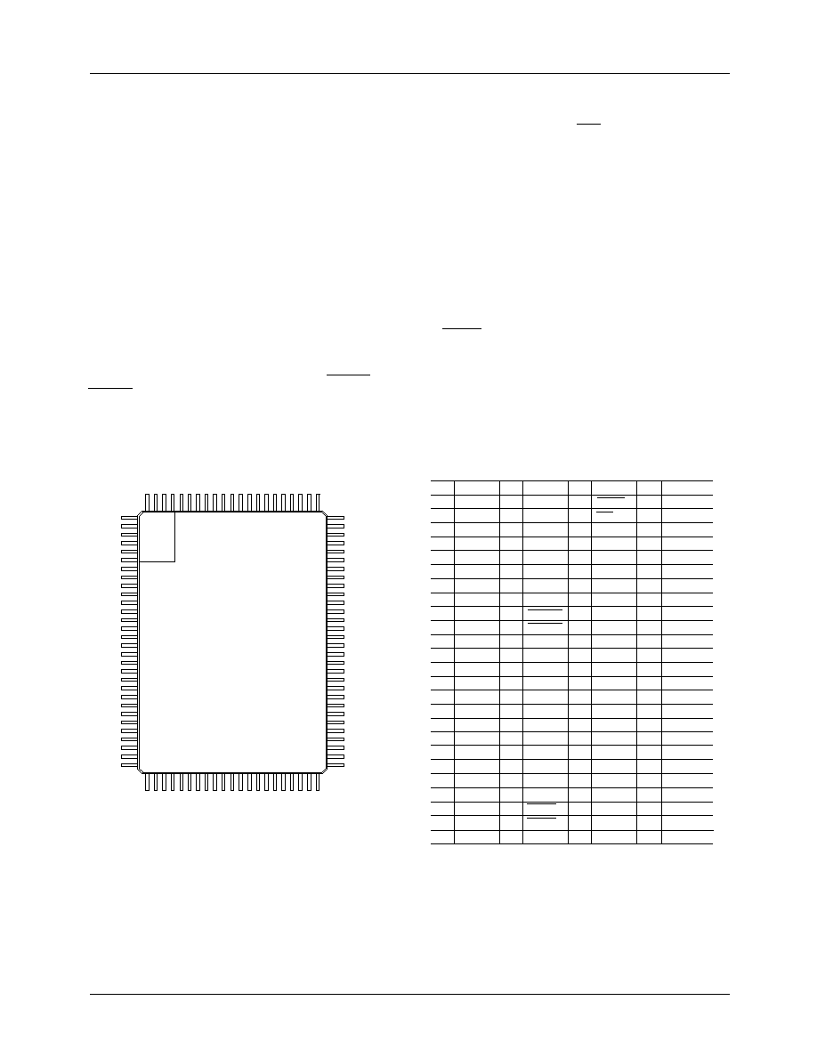
Pin Assignments
G/Y
1
G/Y
0
LDV
GND
V
DD
B/Cb
9
B/Cb
8
B/Cb
7
B/Cb
6
B/Cb
5
B/Cb
4
B/Cb
3
B/Cb
2
B/Cb
1
B/Cb
0
GND
V
DD
R/Cr
9
R/Cr
8
R/Cr
7
R/Cr
6
R/Cr
5
R/Cr
4
R/Cr
3
R/Cr
2
1
2
3
4
5
6
7
8
9
10
11
12
13
14
15
16
17
18
19
20
21
22
23
24
25
R/Cr
1
R/Cr
0
GND
V
DD
DREF
FID
0
FID
1
FID
2
DHSYNC
DVSYNC
D
0
D
1
D
2
GND
V
DD
D
3
D
4
D
5
D
6
D
7
GND
V
DD
HSYNC
VSYNC
BUFFER
26
27
28
29
30
31
32
33
34
35
36
37
38
39
40
41
42
43
44
45
46
47
48
49
50
Pin Name
Pin Name
RESET
SET
SER
SA
0
SA
1
SA
2
GND
SDA
SCL
CS
R/W
A
0
A
1
GND
V
DD
VIDEOB
0
VIDEOB
1
VIDEOB
2
VIDEOB
3
VIDEOB
4
VIDEOB
5
VIDEOB
6
VIDEOB
7
VIDEOB
8
VIDEOB
9
51
52
53
54
55
56
57
58
59
60
61
62
63
64
65
66
67
68
69
70
71
72
73
74
75
GND
VIDEOA
0
VIDEOA
1
VIDEOA
2
VIDEOA
3
VIDEOA
4
VIDEOA
5
VIDEOA
6
VIDEOA
7
VIDEOA
8
VIDEOA
9
MASTER
0
MASTER
1
CLOCK
GND
V
DD
GND
G/Y
9
G/Y
8
G/Y
7
G/Y
6
G/Y
5
G/Y
4
G/Y
3
G/Y
2
76
77
78
79
80
81
82
83
84
85
86
87
88
89
90
91
92
93
94
95
96
97
98
99
100
Pin Name
Pin
Name
1
30
65-22x5y-03
31
50
51
80
81
100