 | –≠–ª–µ–∫—Ç—Ä–æ–Ω–Ω—ã–π –∫–æ–º–ø–æ–Ω–µ–Ω—Ç: TN3467A | –°–∫–∞—á–∞—Ç—å:  PDF PDF  ZIP ZIP |

TN3467A / MMPQ3467
TN3467A
PNP Switching Transistor
This device is designed for high speed saturated switching applications
at currents to 800 mA. Sourced from Process 70.
Absolute Maximum Ratings*
TA = 25∞C unless otherwise noted
*
These ratings are limiting values above which the serviceability of any semiconductor device may be impaired.
NOTES:
1) These ratings are based on a maximum junction temperature of 150 degrees C.
2) These are steady state limits. The factory should be consulted on applications involving pulsed or low duty cycle operations.
Symbol
Parameter
Value
Units
V
CEO
Collector-Emitter Voltage
40
V
V
CBO
Collector-Base Voltage
40
V
V
EBO
Emitter-Base Voltage
5.0
V
I
C
Collector Current - Continuous
1.2
A
T
J
, T
stg
Operating and Storage Junction Temperature Range
-55 to +150
∞
C
MMPQ3467
Thermal Characteristics
TA = 25∞C unless otherwise noted
Symbol
Characteristic
Max
Units
TN3467A
MMPQ3467
P
D
Total Device Dissipation
Derate above 25
∞
C
1.0
8.0
1.0
8.0
W
mW/
∞
C
R
JC
Thermal Resistance, Junction to Case
50
∞
C/W
R
JA
Thermal Resistance, Junction to Ambient
Effective 4 Die
Each Die
125
125
240
∞
C/W
∞
C/W
∞
C/W
TO-226
C
B
E
C
C
C
C
C
C
C
C
SOIC-16
E
B
E
B
E
B
E
B
Discrete POWER & Signal
Technologies
©
1997 Fairchild Semiconductor Corporation

TN3467A / MMPQ3467
PNP Switching Transistor
(continued)
Electrical Characteristics
TA = 25∞C unless otherwise noted
OFF CHARACTERISTICS
SMALL SIGNAL CHARACTERISTICS
Symbol
Parameter
Test Conditions
Min
Max
Units
ON CHARACTERISTICS*
V
(BR)CEO
Collector-Emitter Breakdown Voltage*
I
C
= 10 mA, I
B
= 0
40
V
V
(BR)CBO
Collector-Base Breakdown Voltage
I
C
= 10
µ
A, I
E
= 0
40
V
V
(BR)EBO
Emitter-Base Breakdown Voltage
I
E
= 10
µ
A, I
C
= 0
5.0
V
I
BEV
Base-Cutoff Current
V
CE
= 30 V, V
BE
= 3.0 V
120
nA
I
CEX
Collector-Cutoff Current
V
CE
= 30 V, V
BE
= 3.0 V
100
nA
I
CBO
Collector-Cutoff Current
V
CB
= 30 V, I
E
= 0
V
CB
= 30 V, I
E
= 0, T
A
= 150
∞
C
0.01
15
µ
A
µ
A
SWITCHING CHARACTERISTICS
(except for MMPQ3467)
*
Pulse Test: Pulse Width
300
µ
s, Duty Cycle
1.0%
t
d
Delay Time
V
CC
= 30 V, V
BE
= 2.0 V,
10
ns
t
r
Rise Time
I
C
= 500 mA, I
B1
= 50 mA
30
ns
t
s
Storage Time
V
CC
= 30 V, I
C
= 500 mA,
60
ns
t
f
Fall Time
I
B1
= I
B2
= 50 mA
30
ns
h
FE
DC Current Gain
I
C
= 150 mA, V
CE
= 1.0 V
I
C
= 500 mA, V
CE
= 1.0 V
I
C
= 1.0 A, V
CE
= 5.0 V
40
40
40
120
V
CE(
sat
)
Collector-Emitter Saturation Voltage
I
C
= 150 mA, I
B
= 15 mA
I
C
= 500 mA, I
B
= 50 mA
I
C
= 1.0 A, I
B
= 100 mA
0.3
0.5
1.0
V
V
V
V
BE(
sat
)
Base-Emitter Saturation Voltage
I
C
= 150 mA, I
B
= 15 mA
I
C
= 500 mA, I
B
= 50 mA
I
C
= 1.0 A, I
B
= 100 mA
0.8
1.0
1.2
1.6
V
V
V
f
T
Current Gain-Bandwidth Product
I
C
= 50 mA, V
CE
= 10 V,
f = 100 MHz
175
MHz
C
obo
Output Capacitance
V
CB
= 10 V, I
E
= 0, f = 1.0 KHz
25
pF
C
ibo
Input Capacitance
V
BE
= 0.5 V, I
C
= 0, f = 1.0 KHz
100
pF

TN3467A / MMPQ3467
DC Typical Characteristics
Typical Pulsed Current Gain
vs Collector Current
P
0
0.01
0.1
1
0
20
40
60
80
100
120
140
I - COLLECTOR CURRENT (A)
h
-
T
YPIC
A
L
PU
L
SED
C
U
R
R
EN
T
G
A
IN
FE
C
V = 1V
CE
125 ∫
C
- 40 ∫C
25 ∞C
Collector-Emitter Saturation
Voltage vs Collector Current
P 0
10
100
300
500
0
0.1
0.2
0.3
0.4
I - COLLECTOR CURRENT (mA)
V
-
C
O
LLE
C
T
O
R
-
E
M
I
TTE
R
V
O
L
T
A
G
E
(
V
)
CE
S
A
T
C
= 10
125 ∫
C
- 40 ∫C
25 ∞C
Base-Emitter Saturation
Voltage vs Collector Current
P
0
10
100
1000
0.2
0.4
0.6
0.8
1
I - COLLECTOR CURRENT (mA)
V
-
B
A
SE-
EM
I
T
T
E
R
VO
L
T
A
G
E
(
V
)
B
ESA
T
125 ∫
C
- 40 ∫C
25 ∞C
C
= 10
Base-Emitter ON Voltage vs
Collector Current
P 0
10
100
300
0.4
0.6
0.8
1
I - COLLECTOR CURRENT (mA)
V
-
B
A
SE-
EM
I
T
T
E
R
O
N
VO
L
T
A
G
E
(
V
)
B
E(O
N
)
C
V = 5V
CE
125 ∫
C
- 40 ∫C
25 ∞C
Collector-Cutoff Current
vs Ambient Temperature
25
50
75
100
125
150
1
10
100
1000
6000
T - AMBIENT TEMPERATURE ( C)
I
-
CO
L
L
E
CT
O
R
CURR
E
N
T
(n
A)
A
V = 30V
CB
∫
CBO
PNP Switching Transistor
(continued)
TN3467A / MMPQ3467
PNP Switching Transistor
(continued)
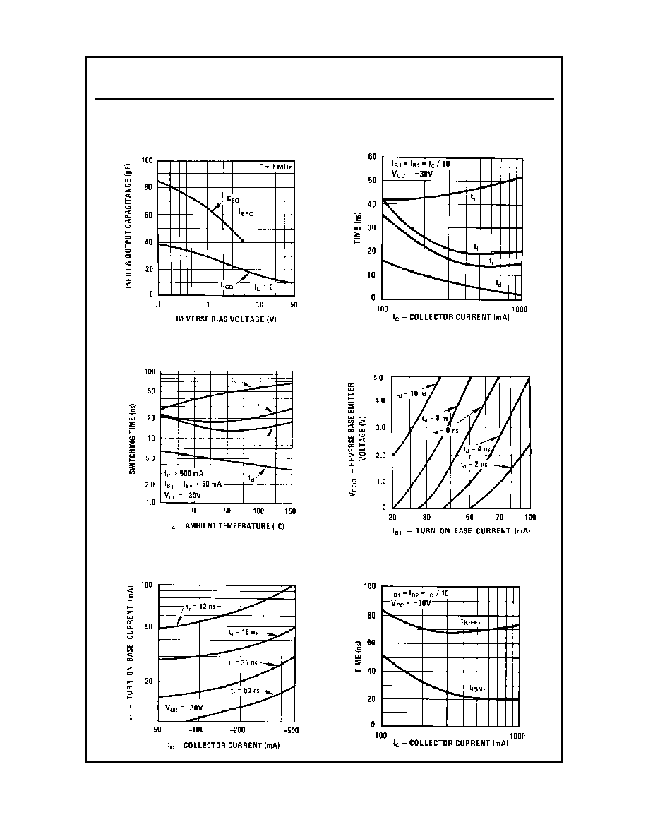
AC Typical Characteristics
Switching Times vs.
Collector Current
Input / Output Capacitance
vs. Reverse Bias Voltage
Switching Times vs.
Ambient Temperature
Delay Time vs. Turn On Base
Current and Reverse Bias
Emitter Voltage
Rise Time vs. Collector Current
and Turn On Base Current
Turn On / Turn Off Times
vs. Collector Current

TN3467A / MMPQ3467
AC Typical Characteristics
(continued)
Fall Time vs. Turn On
and Turn Off Base Currents
Fall Time vs. Turn On
and Turn Off Base Currents
Storage Time vs. Turn On and
Turn Off Base Currents
Storage Time vs. Turn On and
Turn Off Base Currents
PNP Switching Transistor
(continued)