TN5415A
Discrete POWER & Signal
Technologies
PNP High Voltage Amplifier
TN5415A
This device is designed for use as high voltage drivers requiring
collector currents to 100 mA. Sourced from Process 76. See
MPSA92 for characteristics.
Absolute Maximum Ratings*
TA = 25∞C unless otherwise noted
*
These ratings are limiting values above which the serviceability of any semiconductor device may be impaired.
NOTES:
1) These ratings are based on a maximum junction temperature of 150 degrees C.
2) These are steady state limits. The factory should be consulted on applications involving pulsed or low duty cycle operations.
Thermal Characteristics
TA = 25∞C unless otherwise noted
Symbol
Parameter
Value
Units
V
CEO
Collector-Emitter Voltage
200
V
V
CBO
Collector-Base Voltage
200
V
V
EBO
Emitter-Base Voltage
4.0
V
I
C
Collector Current - Continuous
100
mA
T
J
, T
stg
Operating and Storage Junction Temperature Range
-55 to +150
∞
C
Symbol
Characteristic
Max
Units
TN5415A
P
D
Total Device Dissipation
Derate above 25
∞
C
1.0
8.0
W
mW/
∞
C
R
JC
Thermal Resistance, Junction to Case
125
∞
C/W
R
JA
Thermal Resistance, Junction to Ambient
50
∞
C/W
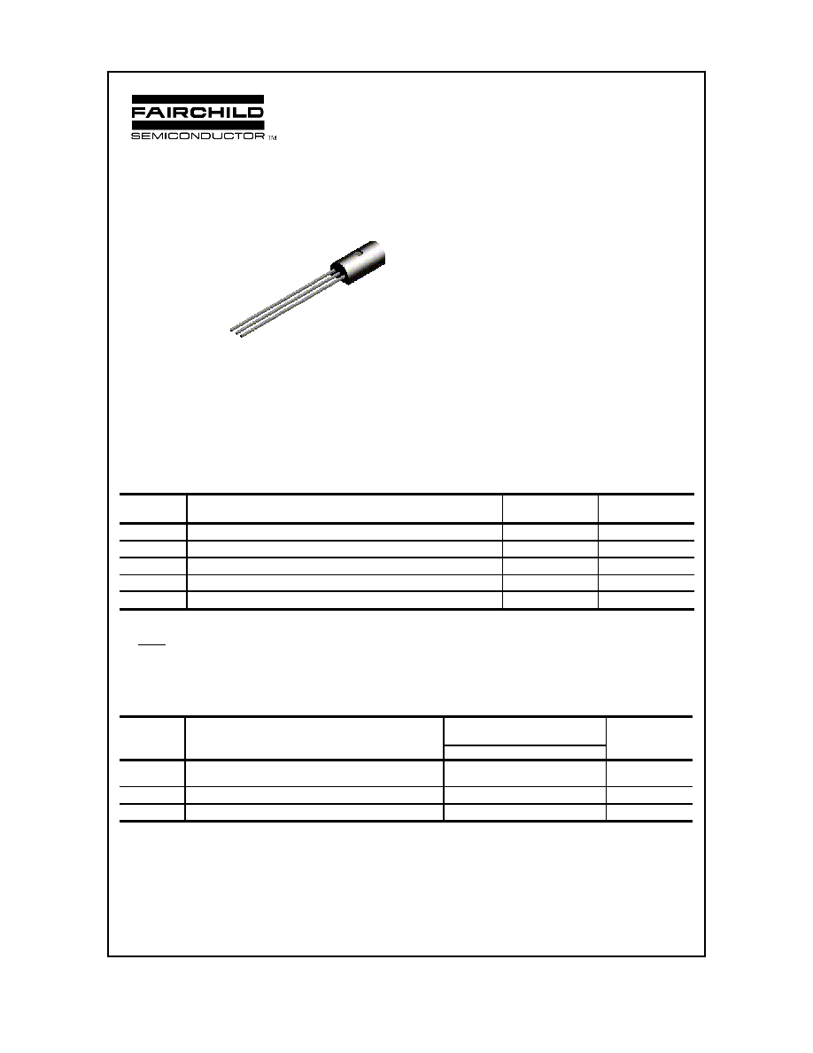
TO-226
C
B
E
©
1997 Fairchild Semiconductor Corporation
TN5415A
PNP High Voltage Amplifier
(continued)
Electrical Characteristics
TA = 25∞C unless otherwise noted
OFF CHARACTERISTICS
Symbol
Parameter
Test Conditions
Min
Max
Units
V
(BR)CEO
Collector-Emitter Breakdown Voltage*
I
C
= 50 mA, I
B
= 0
200
V
V
(BR)CBO
Collector-Base Breakdown Voltage
I
C
= 100
µ
A, I
E
= 0
200
V
V
(BR)EBO
Emitter-Base Breakdown Voltage
I
E
= 100
µ
A, I
C
= 0
4.0
V
I
CBO
Collector Cutoff Current
V
CB
= 175 V
50
µ
A
I
CEX
Collector Cutoff Current
V
CE
= 200 V, V
BE
= 1.5 V (rev)
50
µ
A
I
CEO
Collector Cutoff Current
V
CE
= 150 V
50
µ
A
I
EBO
Emitter Cutoff Current
V
EB
= 4.0 V, I
C
= 0
20
µ
A
ON CHARACTERISTICS*
h
FE
DC Current Gain
V
CE
= 10 V, I
C
= 50 mA
30
150
V
CE(
sat
)
Collector-Emitter Saturation Voltage
I
C
= 50 mA, I
B
= 5.0 mA
2.5
V
V
BE(
on
)
Base-Emitter On Voltage
I
C
= 50 mA, V
CE
= 10 V
1.5
V
SMALL SIGNAL CHARACTERISTICS
C
ob
Output Capacitance
V
CB
= 10 V, f = 1.0 MHz
15
pF
C
ib
Input Capacitance
V
EB
= 5.0 V, f = 1.0 MHz
75
pF
h
fe
Small-Signal Current Gain
I
C
= 5.0 mA, V
CE
= 10 V,
f = 5.0 MHz
I
C
= 5.0 mA, V
CE
= 10 V,
f = 1.0 kHz
3.0
25
Re
(hie)
Input Resistance
V
CE
= 10 V, I
C
= 5.0 mA
300
IS /
b
Safe Operating Area
V
CE
= 100 V, t = 100 mS
100
mA
*
Pulse Test: Pulse Width
300
µ
s, Duty Cycle
2.0%