 | –≠–ª–µ–∫—Ç—Ä–æ–Ω–Ω—ã–π –∫–æ–º–ø–æ–Ω–µ–Ω—Ç: UC3525AN | –°–∫–∞—á–∞—Ç—å:  PDF PDF  ZIP ZIP |

©2000 Fairchild Semiconductor International
www.fairchildsemi.com
Rev. 5.0
Features
∑ 5V
±
1% Reference
∑ Oscillator Sync terminal
∑ Internal Soft Start
∑ Deadtime Control
∑ Under-Voltage Lockout
Description
UC3525A is a monolithic integrated circuit that Included
all of the control circuit necessary for a pulse width modulat-
ing regulator. There are a voltage reference, an error ampli-
fier, a pulse width modulator, an oscillator, under-voltage
lockout, soft start circuit, and output drivers in the chip.
16-DIP
1
Internal Block Diagram
UC3525A
SMPS Controller
UC3525A
2
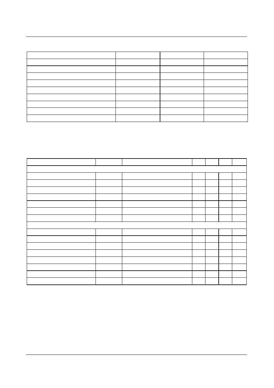
Absolute Maximum Ratings
Electrical Characteristics
(V
CC
= 20V, T
A
= -30
∞
C to + 85
∞
C, unless otherwise specified)
Parameter
Symbol
Value
Unit
Supply Voltage
V
CC
40
V
Collector Supply Voltage
V
C
40
V
Output Current, Sink or Source
I
O
500
mA
Reference Output Current
I
REF
50
mA
Oscillator Charging Current
I
CHG(OSC)
5
mA
Power Dissipation (T
A
= 25
∞
C)
P
D
1000
m/W
Operating Temperature
T
OPR
0 ~ +70
∞
C
Storage Temperature
T
STG
-65 ~ +150
∞
C
Lead Temperature (Soldering, 10 sec)
T
LEAD
+300
∞
C
Parameter
Symbol
Conditions
Min. Typ. Max. Unit
REFERENCE SECTION
Reference Output Voltage
V
REF
T
J
= 25
∞
C
5.0
5.1
5.2
V
Line Regulation
V
REF
V
CC
= 8 to 35V
-
9
20
mV
Load Regulation
V
REF
I
REF
= 0 to 20mA
-
20
50
mV
Short Circuit Output Current
I
SC
V
REF
= 0, T
J
= 25
∞
C
-
80
100
mA
Total Output Variation (Note 1)
V
REF
Line, Load and Temperature
4.95
-
5.25
V
Temperature Stability (Note 1)
ST
T
-
-
20
50
mV
Long Term Stability (Note 1)
ST
T
J
= 125
∞
C ,1 KHR
S
-
20
50
mV
OSCILLATOR SECTION
Initial Accuracy (Note 1, 2)
ACCUR
T
J
= 25
∞
C
-
±
3
±
6
%
Frequency Change With Voltage
f/
V
CC
V
CC
= 8 to 35V (Note 1, 2)
-
±
0.8
±
2
%
Maximum Frequency
f
(MAX)
R
T
= 2K
, C
T
= 470pF
400
430
-
KHz
Minimum Frequency
f
(MIN)
R
T
= 200K
, C
T
= 0.1uF
-
60
120
Hz
Clock Amplitude (Note 1, 2)
V
(CLK)
-
3
4
-
V
Clock Width (Note 1, 2)
t
W(CLK)
T
J
= 25
∞
C
0.3
0.6
1
µ
s
Sync Threshold
V
TH(SYNC)
-
1.2
2
2.8
V
Sync Input Current
I
I(SYNC)
Sync = 3.5V
-
1.3
2.5
mA

UC3525A
3
Electrical Characteristics
(V
CC
= 20V, T
A
= 0 to +85
∞
C, unless otherwise specified)
Notes :
1. These parameters. although guaranteed over the recommended operating conditions, are not 100% tested in production
2. Tested at f
OSC
=40 KHz (R
T
=3.6K, C
T
=0.01uF, R
I
= 0
)
Parameter
Symbol
Conditions
Min. Typ. Max. Unit
ERROR AMPLIFIER SECTION (V
CM
= 5.1V)
Input Offset Voltage
V
IO
-
-
1.5
10
mV
Input Bias Current
I
BIAS
-
-
1
10
µ
A
Input Offset Current
I
IO
-
-
0.1
1
µ
A
Open Loop Voltage Gain
G
VO
R
L
10M
60
80
-
dB
Common Mode Rejection Ratio
CMRR
V
CM
= 1.5 to 5.2V
60
90
-
dB
Power Supply Rejection Ratio
PSRR
V
CC
= 8 to 3.5V
50
60
-
dB
PWM COMPARATOR SECTION
Minimum Duty Cycle
D
(MIN)
-
-
-
0
%
Maximum Duty Cycle
D
(MAX)
-
45
49
-
%
Input Threshold Voltage (Note 2)
V
TH1
Zero Duty Cycle
0.7
0.9
-
V
Input Threshold Voltage (Note 2)
V
TH2
Max Duty Cycle
-
3.2
3.6
V
SOFT-START SECTION
Soft Start Current
I
SOFT
V
SD
= 0V, V
SS
= 0V
25
51
80
µ
A
Soft Start Low Level Voltage
V
SL
V
SD
= 25V
-
0.3
0.7
V
Shutdown Threshold Voltage
V
TH(SD)
-
0.6
0.8
1
V
Shutdown Input Current
I
N(SD)
V
SD
= 2.5V
-
0.3
1
mA
OUTPUT SECTION
Low Output Voltage I
V
OL I
I
SINK
= 20mA
-
0.1
0.4
V
Low Output Voltage II
V
OL II
I
SINK
= 100mA
-
0.05
2
V
High Output Voltage I
V
CH I
I
SOURCE
= 20mA
18
19
-
V
High Output Voltage II
V
CH II
I
SOURCE
= 100mA
17
18
-
V
Under Voltage Lockout
V
UV
V
8
and V
9
= High
6
7
8
V
Collector Leakage Current
I
LKG
V
CC
= 35V
-
80
200
µ
A
Rise Time (Note 1)
t
R
C
L
= 1uF, T
J
= 25
∞
C
-
80
600
ns
Fall Time (Note 1)
t
F
C
L
= 1uF, T
J
= 25
∞
C
-
70
300
ns
STANDBY CURRENT
Supply Current
I
CC
V
CC
= 35V
-
12
20
mA

UC3525A
4
Test Circuit

UC3525A
5
Mechanical Dimensions
Package
#1
#8
#9
#16
6.40
±
0.20
7.62
0.300
2.54
0.100
0.252
±
0.008
0~15
∞
0.25
+0.10
≠0.05
0.010
+0.004
≠0.002
3.30
±
0.30
0.130
±
0.012
3.25
±
0.20
0.128
±
0.008
19.40
±
0.20
0.764
±
0.008
19.80
0.780
MAX
5.08
0.200
0.38
0.014
MAX
MIN
0.81
0.032
()
0.46
±
0.10
0.018
±
0.004
0.059
±
0.004
1.50
±
0.10
16-DIP