© 2005 Fairchild Semiconductor Corporation
DS500893
www.fairchildsemi.com
August 2004
Revised August 2005
U
S
B
1
T1
10
4 U
n
iv
ers
a
l
Seri
al
Bus
Pe
riphera
l T
r
ans
cei
ve
r wit
h V
o
lt
age
Re
gulat
or
USB1T1104
Universal Serial Bus Peripheral Transceiver
with Voltage Regulator
General Description
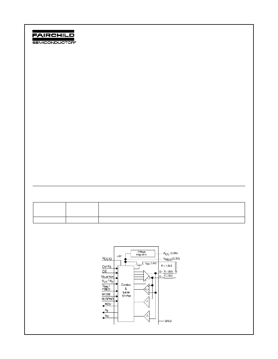
The USB1T1104 is an Universal Serial Bus Specification Rev
2.0 compliant transceiver. The device provides an USB inter-
face for Full-Speed (12Mbit/s) USB applications. The
USB1T1104 provides excellent flexibility, allowing differential
and single ended inputs while an integrated voltage regulator
sets the I/O level to 1.65V to 3.6V. Utilizing an integrated 5.0V to
3.3V voltage regulator, the part can be powered directly from
the USB host (V
BUS
) to minimize the power consumed from the
local sources while used in devices with low supply voltages.
The USB1T1104 provides 15kV ESD protection on the USB bus
pins (D
/D
). This eliminates the need for any external ESD
devices while providing excellent protection to larger and more
expensive ASICs and USB controllers.
Features
O
Complies with Universal Serial Bus Specification 2.0
O
Integrated 5V to 3.3V voltage regulator for powering VBus
O
Utilizes digital inputs and outputs to transmit and receive USB
cable data
O
Supports full speed 12Mbits/s speed data rates
O
Ideal for portable electronic devices
O
15kV contact HBM ESD protection on bus pins
O
3.3mm leadless package
O
Industry standard HBCC footprint is lead-free
Applications
O
Cell phone
O
Digital camera
O
MP3
Ordering Code:
Pb-Free package per JEDEC J-STD-020B.
Logic Diagram
Order
Package
Package Description
Number
Number
USB1T1104MHX
MLP16HB
Pb-Free 16-Terminal Molded Leadless Package (MHBCC), JEDEC MO-217, 3mm Square
www.fairchildsemi.com
2
USB1
T1
1
0
4
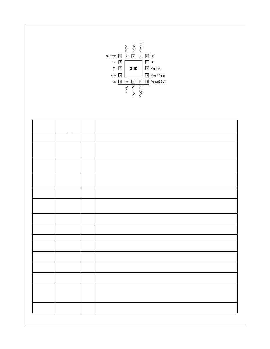
Connection Diagram
(Bottom View)
Terminal Descriptions
Terminal
Number
Terminal
Name
I/O
Terminal Description
1
OE
I
Output Enable: Active LOW enables the transceiver to transmit data on the bus. When not
active the transceiver is in the receive mode (CMOS level is relative to V
CCIO
)
2
RCV
O
Receive Data Output: Non-inverted CMOS level output for USB differential Input (CMOS
output level is relative to V
CCIO
). Driven LOW when SUSPN is HIGH; RCV output is stable
and preserved during SE0 condition.
3
V
p
O
Single-ended D
receiver output V
P
(CMOS level relative to V
CCIO
): Used for external
detection of SEO, error conditions, speed of connected device; Driven HIGH when no
supply connected to V
CC
and V
REG
.
4
V
m
O
Single-ended D
receiver output V
m
(CMOS level relative to V
CCIO
): Used for external
detection of SEO, error conditions, speed of connected device; Driven HIGH when no
supply connected to V
CC
and V
REG
.
5
SUSPND
I
Suspend: Enables a low power state (CMOS level is relative to V
CCIO
).
While the SUSPND pin is active (HIGH) it will drive the RCV pin to logic "0" state.
6
MODE
I
MODE input (CMOS level is relative to V
CCIO
). A HIGH selects the differential input MODE
(V
po
, V
mo
) whereas a LOW enables the single-ended MODE (V
o
, V
FSEO
) see Table 2 and
Table 4
7
V
CCIO
Supply Voltage for digital I/O pins (1.65V to 3.6V): When not connected the D
and D
pins are in 3-STATE. This supply bus is totally independent of V
CC
(5V) and V
REG
(3.3V).
8
Vbusmon
O
Vbus monitor output (CMOS level relative to V
CCIO
): When Vbus
!
4.1V then
Vbusmon = HIGH and when Vbus
3.6V then Vbusmon = LOW.
10, 9
D
, D
AI/O
Data
, Data
: Differential data bus conforming to the USB standard.
11
V
po
/ V
o
I
Driver Data Input (CMOS level is relative to V
CCIO
); Schmitt trigger input; see Table 2 and
Table 3
12
V
mo
/ F
SEO
I
Driver Data Input (CMOS level is relative to V
CCIO
); Schmitt trigger input; see Table 2 and
Table 3
13
V
REG
(3.3V)
Internal Regulator Option: Regulated supply output voltage (3.0V to 3.6V) during 5V oper-
ation; decoupling capacitor of at least 0.1
P
F is required.
14
V
CC
(5.0V)
Internal Regulator Option: Used as supply voltage input (4.0V to 5.5V); can be connected
directly to USB line Vbus.
15
V
PU
(3.3V)
Pull-up Supply Voltage (3.3V
r
10%): Connect an external 1.5k
:
resistor on D
(FS data
rate); Pin function is controlled by Config input pin:
Config = LOW
V
PU
(3.3V) is floating (High Impedance) for zero pull-up current.
Config = HIGH
V
PU
(3.3V) = 3.3V; internally connected to V
REG
(3.3V).
16
Config
I
USB connect or disconnect software control input. Configures 3.3V to external 1.5k
:
resistor on D
when HIGH.
3
www.fairchildsemi.com
USB1
T1
1
0
4
Functional Description
The USB1T1104 transceiver is designed to convert CMOS data
into USB differential bus signal levels and to convert USB differ-
ential bus signal to CMOS data.
To minimize EMI and noise the outputs are edge rate controlled
with the rise and fall times controlled and defined for full speed
data rates. The rise, fall times are balanced between the differ-
ential pins to minimize skew.
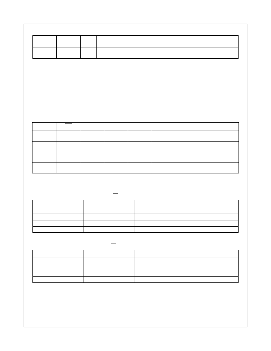
Table 1 describes the specific pin functionality selection.
Table 2, Table 3, and Table 4 describe the specific Truth Tables
for Driver and Receiver operating functions.
The USB1T1104 also has the capability of various power supply
configurations to support mixed voltage supply applications (see
Table 5) and Power Supply Configurations and Options for
detailed descriptions.
Functional Tables
TABLE 1. Function Select
Note 1: Signal levels is function of connection and/or pull-up/pull-down resistors.
Note 2: For SUSPND = HIGH mode the differential receiver is inactive and the output RCV output is forced LOW. The out-of-suspend signaling (K) is detected via the single-
ended receiver outputs of the V
p
and V
m
pins.
TABLE 2. Driver Function (OE = L) using Differential Input Interface Mode Pin = H
Note 3: SE0 = Single Ended Zero
TABLE 3. Driver Function (OE = L) using Single-ended Input Interface Mode Pin = L
Note 4: SE0 = Single Ended Zero
Terminal
Number
Terminal
Name
I/O
Terminal Description
Exposed
Diepad
GND
GND
GND supply down bonded to exposed diepad to be connected to the PCB GND.
SUSPND
OE
D
, D
RCV
V
p
/V
m
Function
L
L
Driving &
Receiving
Active
Active
Normal Driving (Differential Receiver Active)
L
H
Receiving
(Note 1)
Active
Active
Receiving
H
L
Driving
Inactive
(Note 2)
Active
Driving during Suspend
(Differential Receiver Inactive)
H
H
3-STATE
(Note 1)
Inactive
(Note 2)
Active
Low Power State
V
mo
V
po
Data
L
L
SE0 (Note 3)
L
H
Differential Logic 1
H
L
Differential Logic 0
H
H
Illegal State
FSE0
V
o
Data
L
L
Differential Logic 0
L
H
Differential Logic 1
H
L
SE0 (Note 4)
H
H
SE0 (Note 4)
www.fairchildsemi.com
4
USB1
T1
1
0
4
TABLE 4. Receiver Function (OE = H)
X = Don't Care
Power Supply Configurations and Options
The three modes of power supply operation are:
∑ Normal Mode: Regulated Output
1. Regulated Output. V
CCIO
is connected and V
CC
(5.0) is
connected to 5V (4.0V to 5.5V) and the internal voltage
regulator then produces 3.3V for the USB connections.
For normal mode the V
CCIO
is an independent voltage source
(1.65V to 3.6V) that is a function of the external circuit config-
uration.
∑ Sharing Mode: V
CCIO
is only supply connected. V
CC
and
V
REG
are not connected. In this mode the D
and D
pins are
3-STATE and the USB1T1104 allows external signals up to
3.6V to share the D
and D
bus lines. Internally the circuitry
limits leakage from D
and D
pins (maximum 10
P
A) and
V
CCIO
such that device is in low power (suspended) state.
Pins Vbusmon and RCV are forced LOW as an indication of
this mode with Vbusmon being ignored during this state.
∑ Disable Mode: V
CCIO
is not connected and V
CC
(5V) is con-
nected. In this mode the D
and D
pins are 3-STATE and the
device is in low power state.
A summary of the Supply Configurations is described in Table 5.
TABLE 5. Power Supply Configuration Options
Note 5: Hi-Z or forced LOW.
D
, D
RCV
V
p
V
m
Differential Logic 1
H
H
L
Differential Logic 0
L
L
H
SE0
X
L
L
Sharing Mode
L
H
H
Pins
Power Supply Mode Configuration
Sharing
Disable
Normal (Regulated Output)
V
CC
(5V)
3.6V
Connected to 5V Source
Connected to 5V Source
V
REG
(3.3V)
Pulled LOW
Regulator OFF
3.3V, 300
P
A
Regulated Output
3.3V, 300
P
A
Regulated Output
V
CCIO
1.65V to 3.6V Source
Not Connected
1.65V to 3.6V Source
V
PU
(3.3V)
3-STATE (Off)
3-STATE (Off)
3.3V Available if
Config = HIGH
D
, D
3-STATE
3-STATE
Function of
Mode Set Up
V
p
, V
m
H
Invalid
Function of
Mode Set Up
RCV
L
Invalid
Function of
Mode Set Up
OE, SUSPND, Config,
V
po
/V
o
, V
mo
/F
SEO
, MODE
Hi-Z
Hi-Z
Function of
Mode Set Up
5
www.fairchildsemi.com
USB1
T1
1
0
4
Absolute Maximum Ratings
(Note 6)
Recommended Operating Conditions
Note 6: The Absolute Maximum Ratings are those values beyond which the safety of
the device cannot be guaranteed. The device should not be operated at these limits.
The parametric values defined in the Electrical Characteristic tables are not guaran-
teed at the absolute maximum rating. The "Recommended Operating Conditions"
table will define the conditions for actual device operation.
Note 7: IO Absolute Maximum Rating must be observed.
DC Electrical Characteristics
(Supply Pins)
Over recommended range of supply voltage and operating free air temperature (unless otherwise noted).
VCC
(5V) = 4.0V to 5.5V or V
REG
(3.3V) = 3.0V to 3.6V, V
CCIO = 1.65V to 3.6V
Supply Voltage (V
CC
)(5V)
0.5V to
6.0V
I/O Supply Voltage (V
CCIO
)
0.5V to
4.6V
Latch-up Current (I
LU
)
V
I
=
1.8V to
5.4V
150 mA
DC Input Current (I
IK
)
V
I
0
18 mA
DC Input Voltage (V
I
)
(Note 7)
0.5V to V
CCIO
0.5V
DC Output Diode Current (I
OK
)
V
O
!
V
CC
or V
O
0
r
18 mA
DC Output Voltage (V
O
)
(Note 7)
0.5V to V
CCIO
0.5V
Output Source or Sink Current (I
O
)
V
O
= 0 to V
CC
Current for D
, D
Pins
r
12 mA
Current for RCV, V
m
/V
p
r
12 mA
DC V
CC
or GND Current
(I
CC
, I
GND
)
r
100 mA
ESD Immunity Voltage (V
ESD
);
Contact HBM
Pins D
, D
, and GND
15kV
All Other Pins
2.5kV
Storage Temperature (T
STO
)
40
q
C to
125
q
C
Power Dissipation (P
TOT
)
I
CC
(5V)
48 mW
I
CCIO
9 mW
DC Supply Voltage V
CC
(5V)
4.0V to 5.5V
I/O DC Voltage V
CCIO
1.65V to 3.6V
DC Input Voltage Range (V
I
)
0V to V
CCIO
0.5V
DC Input Range for AI/O (V
IA/O
)
0V to 3.6V
Pins D
and D
0V to 3.6V
Operating Ambient Temperature
(T
AMB
)
40
q
C to
85
q
C
Symbol
Parameter
Conditions
Limits
Units
40
q
C to
85
q
C
Min
Typ
Max
V
REG
(3.3V)
Regulated Supply Output
Internal Regulator Option;
3.0
3.3
3.6
V
I
LOAD
d
300
P
A
(Note 8)(Note 9)
I
CC
Operating Supply Current (V
CC
5.0)
Transmitting and Receiving at
4.0
8.0
mA
12 Mbits/s; C
LOAD
= 50 pF (D
, D
)
(Note 10)
I
CCIO
I/O Operating Supply Current
Transmitting and Receiving at
1.0
2.0
mA
12 Mbits/s
(Note 10)
I
CC (IDLE)
Supply Current during
IDLE: V
D
t
2.7V, V
D
d
0.3V;
500
P
A
FS IDLE and SE0 (V
CC
5.0)
SE0: V
D
d
0.3V, V
D
d
0.3V
(Note 11)
I
CCIO (STATIC)
I/O Static Supply Current
IDLE, SUSPND or SE0
20.0
P
A
I
CC(SUSPND)
Suspend Supply Current
SUSPND = HIGH
25.0
P
A
USB1T1104
OE = HIGH
(Note 11)
V
m
= V
p
= OPEN
I
CCIO(SHARING)
I/O Sharing Mode Supply Current
V
CC
(5V) Not Connected
20.0
P
A
www.fairchildsemi.com
6
USB1
T1
1
0
4
DC Electrical Characteristics
(Continued)
Note 8: I
LOAD
includes the pull-up resistor current via pin V
PU
Note 9: The minimum voltage in Suspend mode is 2.7V.
Note 10: Not tested in production, value based on characterization.
Note 11: Excludes any current from load and V
PU
current to the 1.5k
:
resistor.
Note 12: Includes current between V
pu
and the 1.5k internal pull-up resistor.
Note 13: When V
CCIO
2.7V, minimum value for V
REGTH
= 2.0V for supply present condition.
DC Electrical Characteristics
(Digital Pins ≠ excludes D
, D
Pins)
Over recommended range of supply voltage and operating free air temperature (unless otherwise noted). VCCIO = 1.6V to 3.6V
Note 14: If V
CCIO
t
V
REG
then leakage current will be higher than specified.
Symbol
Parameter
Conditions
Limits
Units
40
q
C to
85
q
C
Min
Typ
Max
I
D
r
(SHARING)
Sharing Mode Load Current on
V
CC
(5V) Not Connected
10.0
P
A
D
/D
Pins
Config = LOW; V
D
r
= 3.6V
V
CCTH
V
CC
Threshold Detection Voltage
1.65V
d
V
CCIO
d
3.6V
V
Supply Lost
3.6
Supply Present
4.1
V
CCHYS
V
CC
Threshold Detection
V
CCIO
= 1.8V
70.0
mV
Hysteresis Voltage
V
CCIOTH
V
CCIO
Threshold Detection Voltage
2.7V
d
V
REG
d
3.6V
V
Supply Lost
0.5
Supply Present
1.4
V
CCIOHYS
V
CCIO
Threshold Detection
V
REG
= 3.3V
450
mV
Hysteresis Voltage
Symbol
Parameter
Test Conditions
Limits
Units
40
q
C to
85
q
C
Min
Max
Input Levels
V
IL
LOW Level Input Voltage
0.3
V
V
IH
HIGH Level Input Voltage
0.6*V
CCIO
V
V
HYS
Hysteresis Voltage P11
P12
Pins V
po
/V
mo
, V
CCIO
= 3.3V
0.30
0.7
V
Output Levels
V
OL
LOW Level Output Voltage
I
OL
= 2 mA
0.4
V
I
OL
= 100
P
A
0.15
V
OH
HIGH Level Output Voltage
I
OH
= 2 mA
V
CCIO
- 0.4
V
I
OH
= 100
P
A
V
CCIO
- 0.15
Leakage Current
I
LI
Input Leakage Current
V
CCIO
= 1.65V to 3.6V
r
1.0
(Note 14)
P
A
Capacitance
C
IN
, C
I/O
Input Capacitance
Pin to GND
10.0
pF
7
www.fairchildsemi.com
USB1
T1
1
0
4
DC Electrical Characteristics
(Analog I/O Pins ≠ D
, D
Pins)
Over recommended range of supply voltage and operating free air temperature (unless otherwise noted). VCC
= 4.0V to 5.5V or V
REG = 3.0V to 3.6V
Note 15: V
OH
min. = V
REG
- 0.2V.
Note 16: Includes external resistors of 29
:
on both D
and D
pins.
Note 17: This voltage is available at pin V
PU
and V
REG
.
Note 18: Minimum voltage is 2.7V in the suspend mode.
Symbol
Parameter
Test Condition
Limits
Units
40
q
C to
85
q
C
Min
Typ
Max
Input Levels ≠ Differential Receiver
V
DI
Differential Input Sensitivity
| V
I(D
)
- V
I(D
)
|
0.2
V
V
CM
Differential Common Mode Voltage
0.8
2.5
V
Input Levels ≠ Single-ended Receiver
V
IL
LOW Level Input Voltage
0.8
V
V
IH
HIGH Level Input Voltage
2.0
V
V
HYS
Hysteresis Voltage
0.4
0.7
V
Output Levels
V
OL
LOW Level Output Voltage
R
L
= 1.5k
:
to 3.6V
0.3
V
V
OH
HIGH Level Output Voltage
R
L
= 15k
:
to GND
2.8
(Note 15)
3.6
V
Leakage Current
I
LZ
Input Leakage Current Off State
OE = H
r
1.0
P
A
Capacitance
C
I/O
I/O Capacitance
Pin to GND
20.0
pF
Resistance
Z
DRV
Driver Output Impedance
34.0
41.0
(Note 16)
44.0
:
Z
IN
Driver Input Impedance
10.0
M
:
R
SW
Switch Resistance
10.0
:
V
TERM
Termination Voltage
R
PU
Upstream Port
3.0
(Note 17)
(Note 18)
3.6
V
www.fairchildsemi.com
8
USB1
T1
1
0
4
AC Electrical Characteristics
(A I/O Pins Full Speed)
Over recommended range of supply voltage and operating free air temperature (unless otherwise noted).
VCC
= 4.0V to 5.5V or V
REG
= 3.0V to 3.6V, V
CCIO
= 1.65V to 3.6V, C
L
= 50 pF; R
L
= 1.5K on D
to V
PU
Note 19: Not production tested, guaranteed by characterization.
Symbol
Parameter
Test Conditions
Limits
Unit
40
q
C to
85
q
C
Min
Typ
Max
Driver Characteristics
t
FR
Output Rise Time
C
L
= 50
125 pF
4.0
20.0
ns
10% to 90%
t
FF
Output Fall Time
Figures 1, 5
4.0
20.0
f
RFM
Rise/Fall Time Match
t
F
/ t
R
Excludes First Transition from Idle State
90.0
111.1
%
V
CRS
Output Signal Crossover Voltage
Excludes First Transition from Idle State
1.3
2.0
V
(Note 19)
see Waveform
Driver Timing
t
PLH
Propagation Delay
Figures 2, 5
18.0
ns
t
PHL
(V
p
/V
po
, V
m
/V
mo
to D
/D
)
t
PHZ
Driver Disable Delay
Figures 4, 6
15.0
ns
t
PLZ
(OE to D
/D
)
t
PZH
Driver Enable Delay
Figures 4, 6
15.0
ns
t
PZL
(OE to D
/D
)
Receiver Timing
t
PLH
Propagation Delay (Diff)
Figures 3, 7
15.0
ns
t
PHL
(D
/D
to Rev)
t
PLH
Single Ended Receiver Propagation Delay
Figures 3Figure 7
18.0
ns
t
PHL
(D
/D
to V
p
/ V
po
, V
m
/V
mo
)
9
www.fairchildsemi.com
USB1
T1
1
0
4
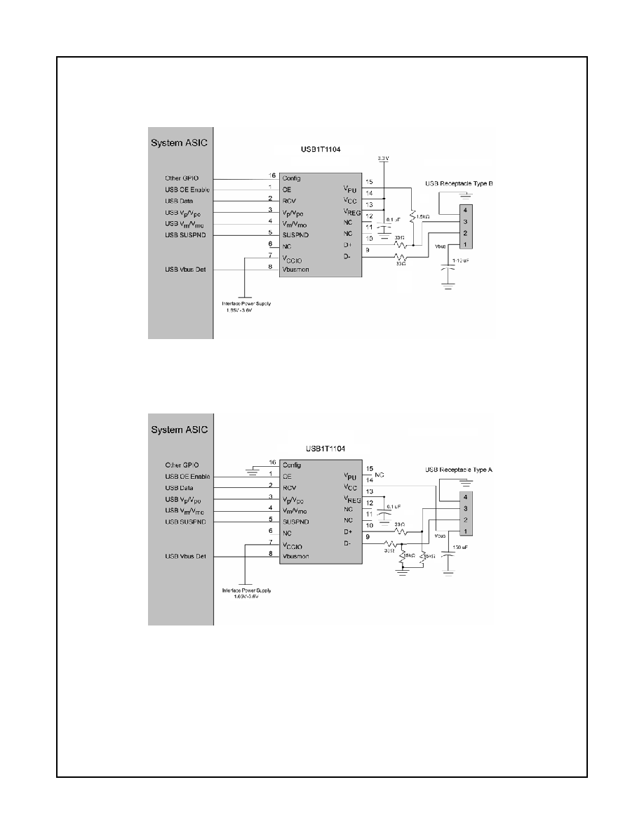
Typical Application Configurations
Upstream Connection in Bypass Mode with Differential Outputs
Downstream Connection in Normal Mode with Differential Outputs
www.fairchildsemi.com
10
USB1
T1
1
0
4
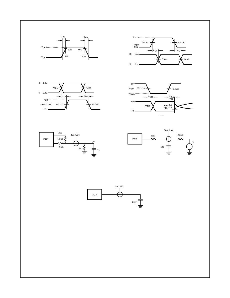
AC Waveforms
FIGURE 1. Rise and Fall Times
FIGURE 2. V
po
/V
o
, V
mo
/V
SEO
to D
/D
FIGURE 3. D
/D
to R
CV
, V
p
and V
m
FIGURE 4. OE to D
/D
Test Circuits and Waveforms
C
L
= 50 pF Full Speed Propagation Delays
C
L
=
125 pF Edge Rates only
FIGURE 5. Load for D
/D
V = 0 for t
PZH
, t
PHZ
V = V
REG
for t
PZL
FIGURE 6. Load for Enable and Disable Times
FIGURE 7. Load for V
m
/V
mo
, V
p/
V
po
and RCV
11
www.fairchildsemi.com
USB1
T1
1
0
4
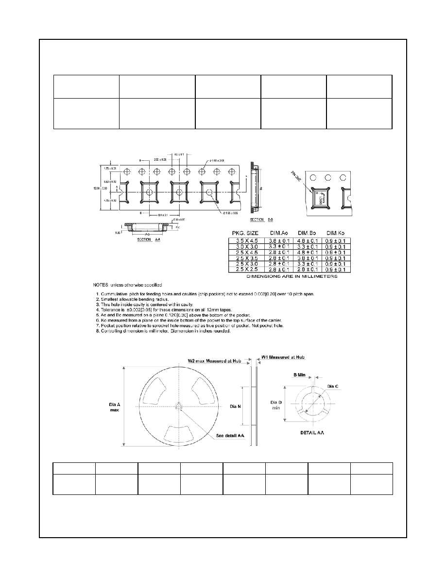
Tape and Reel Specification
Tape Format for MHBCC
TAPE DIMENSIONS inches (millimeters)
REEL DIMENSIONS inches (millimeters)
Package
Tape
Number
Cavity
Cover Tape
Designator
Section
Cavities
Status
Status
Leader (Start End)
125 (typ)
Empty
Sealed
MHX
Carrier
2500/3000
Filled
Sealed
Trailer (Hub End)
75 (typ)
Empty
Sealed
Tape Size
A
B
C
D
N
W1
W2
12 mm
13.0
0.059
0.512
0.795
7.008
0.488
0.724
330
(1.50)
(13.00)
(20.20)
(178)
(12.4)
(18.4)
www.fairchildsemi.com
12
USB1
T1
1
0
4
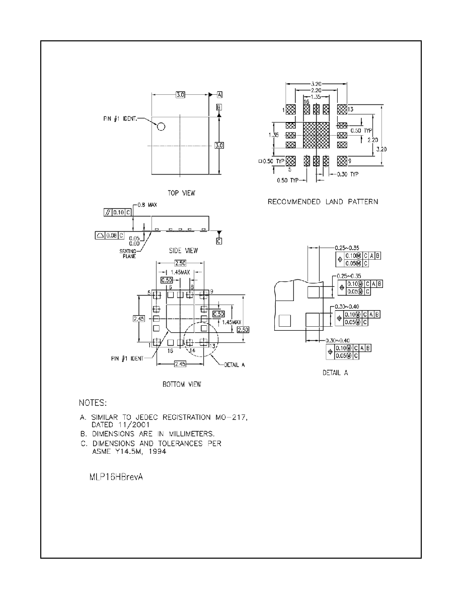
Physical Dimensions
inches (millimeters) unless otherwise noted
Pb-Free 16-Terminal Molded Leadless Package (MHBCC), JEDEC MO-217, 3mm Square
Package Number MLP16HB
13
www.fairchildsemi.com
U
S
B
1
T1
10
4 U
n
iv
ers
a
l
Seri
al
Bus
Pe
riphera
l T
r
ans
cei
ve
r wit
h V
o
lt
age
Re
gulat
or
DISCLAIMER
FAIRCHILD SEMICONDUCTOR RESERVES THE RIGHT TO MAKE CHANGES WITHOUT FURTHER NOTICE TO ANY
PRODUCTS HEREIN TO IMPROVE RELIABILITY, FUNCTION OR DESIGN. FAIRCHILD DOES NOT ASSUME ANY LIABILITY
ARISING OUT OF THE APPLICATION OR USE OF ANY PRODUCT OR CIRCUIT DESCRIBED HEREIN; NEITHER DOES IT
CONVEY ANY LICENSE UNDER ITS PATENT RIGHTS, NOR THE RIGHTS OF OTHERS.
LIFE SUPPORT POLICY
FAIRCHILD'S PRODUCTS ARE NOT AUTHORIZED FOR USE AS CRITICAL COMPONENTS IN LIFE SUPPORT DEVICES
OR SYSTEMS WITHOUT THE EXPRESS WRITTEN APPROVAL OF FAIRCHILD SEMICONDUCTOR CORPORATION
As used herein:
1. Life support devices or systems are devices or systems
which, (a) are intended for surgical implant into the body, or
(b) support or sustain life, or (c) whose failure to perform
when properly used in accordance with instructions for use
provided in the labeling, can be reasonably expected to
result in significant injury to the user.
2. A critical component is any component of a life support
device or system whose failure to perform can be reason-
ably expected to cause the failure of the life support device
or system, or to affect its safety or effectiveness.
PRODUCT STATUS DEFINITIONS
Definition of terms
Datasheet Identification Product Status
Definition
Advance Information
Formative or In Design
This datasheet contains the design specifications for product develop-
ment. Specifications may change in any manner without notice.
Preliminary
First Production
This datasheet contains preliminary data, and supplementary data will
be published at a later date. Fairchild Semiconductor reserves the right
to make changes at any time without notice in order to improve design.
No Identification Needed
Full Production
This datasheet contains final specifications. Fairchild Semiconductor
reserves the right to make changes at any time without notice in order
to improve design.
Obsolete
Not In Production
This datasheet contains specifications on a product that has been dis-
continued by Fairchild Semiconductor. The datasheet is printed for ref-
erence information only.