© 2005 Fairchild Semiconductor Corporation
DS500894
www.fairchildsemi.com
September 2004
Revised January 2005
USB1
T20
Unive
r
sal
Ser
i
al
Bus
T
r
a
n
sceive
r
USB1T20
Universal Serial Bus Transceiver
General Description
The USB1T20 is a generic USB 2.0 compliant transceiver.
Using a single voltage supply, the USB1T20 provides an
ideal USB interface solution for any electronic device able
to supply 3.0V to 3.6V. It is designed to allow 5.0V or 3.3V
programmable and standard logic to interface with the
physical layer of the Universal Serial Bus. It is capable of
transmitting and receiving serial data at both full speed
(12Mbit/s) and low speed (1.5Mbit/s) data rates.
Packaged in industry standard TSSOP and Fairchild's
ultra-small 2.5mm x 2.5mm MLP package, the USB1T20 is
ideal for ultra-portable electronics and other space con-
strained applications.
Features
s
Complies with Universal Serial Bus specification 2.0 for
FS/LS applications
s
Utilizes digital inputs and outputs to transmit and receive
USB cable data
s
Supports 12Mbit/s "Full Speed" and 1.5Mbit/s
"Low Speed" serial data transmission
s
Supports single-ended and differential data interface as
function of MODE
s
Single 3.3V supply
s
ESD Performance: Human Body Model
>
9.5 kV on D
-
, D
+
pins only
>
4 kV on all other pins
s
Space saving 14-terminal MLP package
Ordering Code:
Note 1: Devices also available in Tape and Reel. Specify by appending the suffix letter "X" to the ordering code.
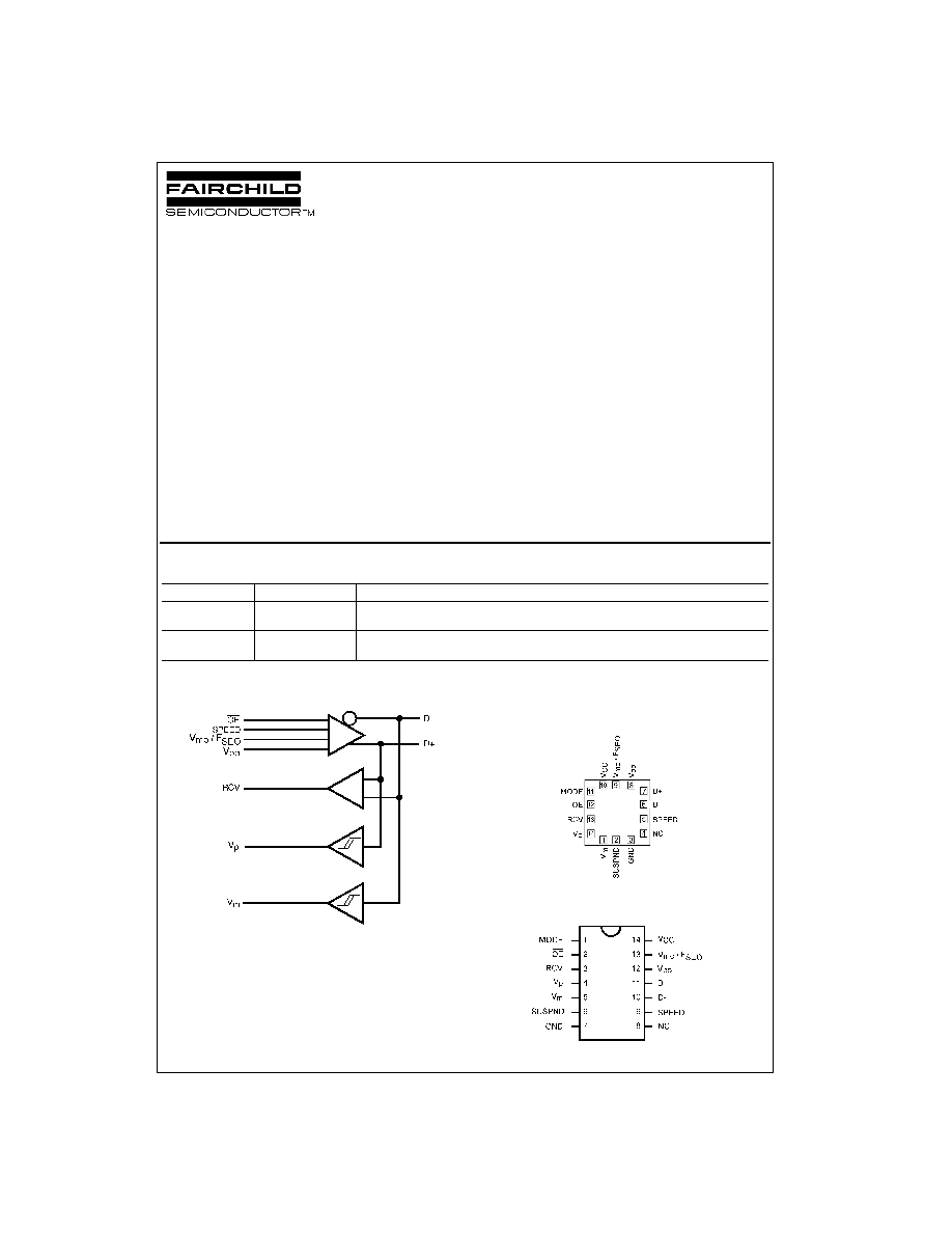
Logic Diagram
Connection Diagrams
Terminal Assignments for MLP (Preliminary)
(Top View)
Pin Assignments for TSSOP
(Top View)
Order Number
Package Number
Package Description
USB1T20MPX
(Preliminary)
MLP14D
14-Terminal Molded Leadless Package (MLP), 2.5mm Square
USB1T20MTC
(Note 1)
MTC14
14-Lead Thin Shrink Small Outline Package (TSSOP), JEDEC MO-153, 4.4mm Wide
www.fairchildsemi.com
2
USB
1
T20
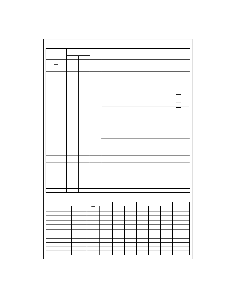
Terminal and Pin Descriptions
Functional Truth Table
X
=
Don't Care
Z
=
3-STATE
U
=
Undefined State
Terminal or Pin
Name
Terminal or Pin
Number
I/O
Description
MLP14D MTC14
RCV
13
3
O
Receive data. CMOS level output for USB differential input
OE
12
2
I
Output Enable. Active LOW, enables the transceiver to transmit data on the
bus. When not active the transceiver is in receive mode.
MODE
11
1
I
Mode. When left unconnected, a weak pull-up transistor pulls it to
V
CC
and in this GND, the V
mo
/F
SEO
pin takes the function of F
SEO
(Force SEO).
V
po
,
8, 9
12, 13
I
Inputs to differential driver. (Outputs from SIE).
V
mo
/ F
SEO
MODE
V
po
V
mo
/F
SEO
RESULT
0
0
0
Logic "0"
0
1
SE0
1
0
Logic "1"
1
1
SE0
1
0
0
SE0
0
1
Logic "0"
1
0
Logic "1"
1
1
Illegal code
V
p
, V
m
14, 1
4, 5
O
Gated version of D
-
and D
+
. Outputs are logic "0" and logic "1". Used to
detect single ended zero (SE0), error conditions, and interconnect speed.
(Input to SIE).
V
p
V
m
RESULT
0
0
SE0
0
1
Low Speed
1
0
Full Speed
1
1
Error
D
+
, D
-
7, 6
11, 10
AI/O
Data
+
, Data
-
. Differential data bus conforming to the Universal Serial Bus
standard.
SUSPND
2
6
I
Suspend. Enables a low power state while the USB bus is inactive. While
the SUSPND pin is active it will drive the RCV pin to a logic "0" state. Both
D
+
and D
-
are 3-STATE.
SPEED
5
9
I
Edge rate control. Logic "1" operates at edge rates for "full speed".
Logic "0" operates edge rates for "low speed".
V
CC
10
14
--
3.0V to 3.6V power supply
GND
3
7
--
Ground reference
NC
4
8
No Connect
Input
I/O
Outputs
Mode
V
po
V
mo
/F
SEO
OE
SUSPND
D
+
D
-
RCV
V
p
V
m
Result
0
0
0
0
0
0
1
0
0
1
Logic 0
0
0
1
0
0
0
0
U
0
0
SE0
0
1
0
0
0
1
0
1
1
0
Logic 1
0
1
1
0
0
0
0
U
0
0
SE0
1
0
0
0
0
0
0
U
0
0
SE0
1
0
1
0
0
0
1
0
0
1
Logic 0
1
1
0
0
0
1
0
1
1
0
Logic 1
1
1
1
0
0
1
1
U
U
U
Illegal Code
X
X
X
1
0
Z
Z
U
U
U
D
+
/D
-
Hi-Z
X
X
X
1
1
Z
Z
U
U
U
D
+
/D
-
Hi-Z

3
www.fairchildsemi.com
USB1
T20
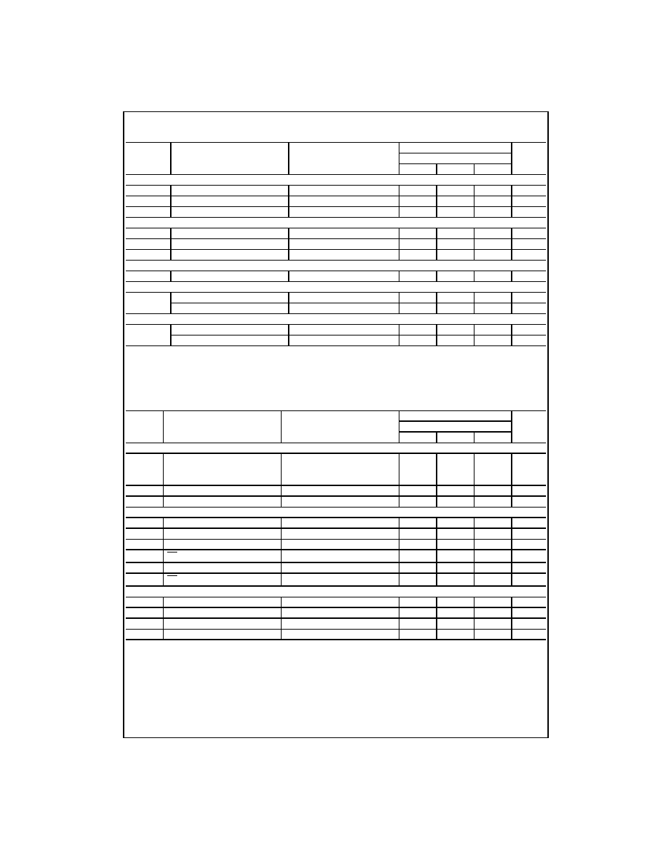
Absolute Maximum Ratings
(Note 2)
Recommended Operating
Conditions
Note 2: The Absolute Maximum Ratings are those values beyond which
the safety of the device cannot be guaranteed. The device should not be
operated at these limits. The parametric values defined in the Electrical
Characteristic tables are not guaranteed at the absolute maximum rating.
The "Recommended Operating Conditions" table will define the conditions
for actual device operation.
Note 3: The input and output voltage ratings may be exceeded if the input
and output clamp current ratings are observed.
DC Electrical Characteristics
(Digital Pins)
Over recommended range of supply voltage and operating free air temperature (unless otherwise noted). V
CC
=
3.0V to 3.6V
DC Supply Voltage (V
CC
)
-
0.5V to
+
7.0V
DC Input Diode Current (I
IK
)
V
I
<
0
-
50 mA
Input Voltage (V
I
)
(Note 3)
-
0.5V to
+
5.5V
Input Voltage (V
I/O
)
-
0.5V to V
CC
+
0.5V
Output Diode Current (I
OK
)
V
O
>
V
CC
or V
O
<
0
±
50 mA
Output Voltage (V
O
)
(Note 3)
-
0.5V to V
CC
+
0.5V
Output Source or Sink Current (I
O
)
V
p
.V
m
, RCV Pins
V
O
=
0V to V
CC
±
15 mA
Output Source or Sink Current (I
O
)
D
+
/D
-
Pins
V
O
=
0V to V
CC
±
50 mA
V
CC
or GND Current (I
CC
, I
GND
)
±
100 mA
Storage Temperature (T
STO
)
-
60
∞
C to
+
150
∞
C
Supply Voltage V
CC
3.0V to 3.6V
Input Voltage (V
I
)
0V to 5.5V
Input Range for AI/O (V
AI/O
)
0V to V
CC
Output Voltage (V
O
)
0V to V
CC
Operating Ambient Temperature
in Free Air (T
AMB
)
-
40
∞
C to
+
85
∞
C
Symbol
Parameter
Test Conditions
Limits
Unit
Temperature
=
-
40
∞
C to
+
85
∞
C
Min
Typ
Max
Input Levels
V
IL
LOW Level Input Voltage
0.8
V
V
IH
HIGH Level Input Voltage
2.0
V
Output Levels
V
OL
LOW Level Output Voltage
I
OL
=
4 mA
0.4
V
I
OL
=
20
µ
A
0.1
V
OH
HIGH Level Output Voltage
I
OH
=
4 mA
2.4
V
I
OH
=
20
µ
A
V
CC
≠ 0.1
Leakage Current
I
L
Input Leakage Current
V
CC
=
3.0 to 3.6
±
5
µ
A
I
CCFS
Supply Current (Full Speed)
V
CC
=
3.0 to 3.6
5
mA
I
CCLS
Supply Current (Low Speed)
V
CC
=
3.0 to 3.6
5
mA
I
CCQ
Quiescent Current
V
CC
=
3.0 to 3.6
5
mA
V
IN
=
V
CC
or GND
I
CCS
Supply Current in Suspend
V
CC
=
3.0 to 3.6; Mode
=
V
CC
10
µ
A
www.fairchildsemi.com
4
USB
1
T20
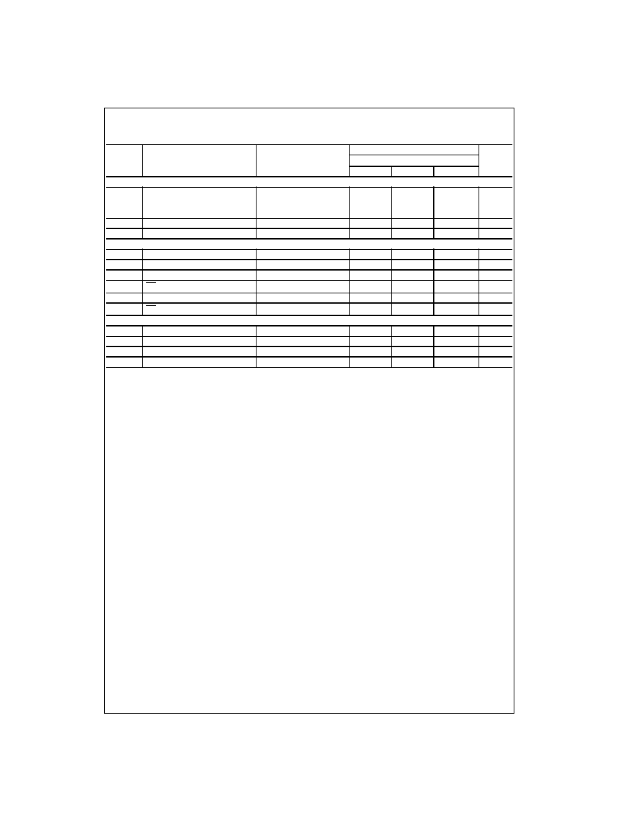
DC Electrical Characteristics
(D
+
/D
-
Pins)
Over recommended range of supply voltage and operating free air temperature (unless otherwise noted). V
CC
=
3.0V to 3.6V
Note 4: Excludes external resistor. In order to comply with USB Specification 1.1, external series resistors of 24
±
1% each on D
+
and D
-
are recom-
mended. This specification is guaranteed by design and statistical process distribution.
Note 5: This specification is guaranteed by design and statistical process distribution.
AC Electrical Characteristics
(D
+
/D
-
Pins, Full Speed)
Over recommended range of supply voltage and operating free air temperature (unless otherwise noted).
V
CC
=
3.0V to 3.6V; C
L
=
50 pF; R
L
=
1.5 k
on D
+
to V
CC
Symbol
Parameter
Test Conditions
Limits
Units
Temperature
=
-
40
∞
C to
+
85
∞
C
Min
Typ
Max
Input Levels
V
DI
Differential Input Sensitivity
|(D
+
) ≠ (D
-
)|
0.2
V
V
CM
Differential Common Mode Range
Includes V
DI
Range
0.8
2.5
V
V
SE
Single Ended Receiver Threshold
0.8
2.0
V
Output Levels
V
OL
Static Output LOW Voltage
R
L
of 1.5 k
to 3.6V
0.3
V
V
OH
Static Output HIGH Voltage
R
L
of 15 k
to GND
2.8
3.6
V
V
CR
Differential Crossover
1.3
2.0
V
Leakage Current
I
OZ
High Z State Data Line Leakage Current 0V
<
V
IN
<
3.3V
±
5
µ
A
Capacitance
C
IN
Transceiver Capacitance
Pin-to-GND
10
pF
(Note 5)
Capacitance Match
10
%
Output Resistance
Z
DRV
Driver Output Resistance
Steady State Drive
4
20
(Note 4)
Resistance Match
10
%
Symbol
Parameter
Test Condition
Limits
Units
Temperature
=
-
40
∞
C to
+
85
∞
C
Min
Typ
Max
Driver Characteristics
10% and 90%
ns
t
R
Rise Time
Figure 1
4
20
t
F
Fall Time
Figure 1
4
20
t
RFM
Rise/Fall Time Matching
(t
R
/t
F
)
90
110
%
V
CRS
Output Signal Crossover Voltage
1.3
2.0
V
Driver Timings
t
PLH
Driver Propagation Delay
Figure 2
18
ns
t
PLH
(V
po
, V
mo
/F
SEO
to D
+
/D
-
)
Figure 2
18
ns
t
PHZ
Driver Disable Delay
Figure 4
13
ns
t
PLZ
(OE to D
+
/D
-
)
Figure 4
13
ns
t
PZH
Driver Enable Delay
Figure 4
17
ns
t
PZL
(OE to D
+
/D
-
)
Figure 4
17
ns
Receiver Timings
t
PLH
Receiver Propagation Delay
Figure 3
16
ns
t
PHL
(D
+
, D
-
to RCV)
Figure 3
19
ns
t
PLH
Single-ended Receiver Delay
Figure 3
8
ns
t
PHL
(D
+
, D
-
to V
p
, V
m
)
Figure 3
8
ns
5
www.fairchildsemi.com
USB1
T20
AC Electrical Characteristics
(D
+
/D
-
Pins, Low Speed)
Over recommended range of supply voltage and operating free air temperature (unless otherwise noted).
V
CC
=
3.0V to 3.6V; C
L
=
200 pF to 600 pF; R
L
=
1.5k
on D
-
to V
CC
Symbol
Parameter
Test Conditions
Limits
Unit
T
AMB
=
-
40
∞
C to
+
85
∞
C
Min
Typ
Max
Driver Characteristics
10% and 90%
ns
t
LR
Rise Time
Figure 1
75
300
t
LF
Fall Time
Figure 1
75
300
t
RFM
Rise/Fall Time Matching
(t
R
/t
F
)
80
120
%
V
CRS
Output Signal Crossover Voltage
1.3
2.0
V
Driver Timings
t
PLH
Driver Propagation Delay
Figure 2
300
ns
t
PHL
(V
po
, V
mo
/F
SEO
to D
+
/D
-
)
Figure 2
300
ns
t
PHZ
Driver Disable Delay
Figure 4
13
ns
t
PLZ
(OE to D
+
/D
-
)
Figure 4
13
ns
t
PZH
Driver Enable Delay
Figure 4
205
ns
t
PZL
(OE to D
+
/D
-
)
Figure 4
205
ns
Receiver Timings
t
PLH
Receiver Propagation Delay
Figure 3
18
ns
t
PHL
(D
+
, D
-
to RCV)
Figure 3
18
ns
t
PLH
Single-ended Receiver Delay
Figure 3
28
ns
t
PHL
(D
+
, D
-
to V
p
, V
m
)
Figure 3
28
ns