 | –≠–ª–µ–∫—Ç—Ä–æ–Ω–Ω—ã–π –∫–æ–º–ø–æ–Ω–µ–Ω—Ç: V320 | –°–∫–∞—á–∞—Ç—å:  PDF PDF  ZIP ZIP |
April 1998
Revised October 1998
V32
0
8-
Bit
Regi
st
ered
Bus T
r
anscei
ver
© 1998 Fairchild Semiconductor Corporation
DS500149.prf
www.fairchildsemi.com
V320
8-Bit Registered Bus Transceiver
General Description
The V320 is an 8-bit universal bus transceiver designed for
high speed interfacing with the VME320 backplane. It has
output characteristics optimized for driving large capacitive
loads and features modified input levels (V
IH
/V
IL
) for
increased noise immunity and reduced input skew. The
V320 functionality consists of bus transceiver circuits with
3-STATE, D-type flip-flops, and control circuitry arranged
for multiplexed transmission of data directly from the input
bus or from the internal registers. Data on the A or B bus
will be clocked into the registers as the appropriate clock
pin goes to a high logic level. OE and direction pins are
provided to control the transceiver function. In the trans-
ceiver mode, data present at the high impedance port may
be stored in either the A or B register or in both. The select
controls can multiplex stored and real time (transparent
mode) data. The direction control determines which bus
will receive data when the enable control OE is active
LOW. In the isolation mode (OE HIGH) A data may be
stored in the B register and/or B data may be stored in the
A register.
Features
s
Independent registers for A and B buses
s
Multiplexed real-time and stored data
s
Guaranteed output skew
s
Guaranteed MOS (Multiple Output Switching) Specifica-
tions
s
Output switching specified for both 50 pF and 250 pF,
and 500 pF loads
s
Guaranteed simultaneous switching noise level (V
OLP
/
V
OLV
) and dynamic threshold performance (V
IHD
/V
ILD
)
s
Glitch free power up/down high impedance for live inser-
tion
s
BiCMOS technology for high drive and low power dissi-
pation
s
-
40
∞
C to 85
∞
C commercial temperature and V
CC
specifi-
cations
s
Modified specifications across V
CC
and temperature
(V
CC
=
5.0V
±
1%, T
=
25
∞
C
±
20
∞
C) present more realis-
tic system conditions
s
Available in TSSOP (MTC)
Ordering Code:
Device also available in Tape and Reel. Specify by appending suffix letter "X" to the ordering code.
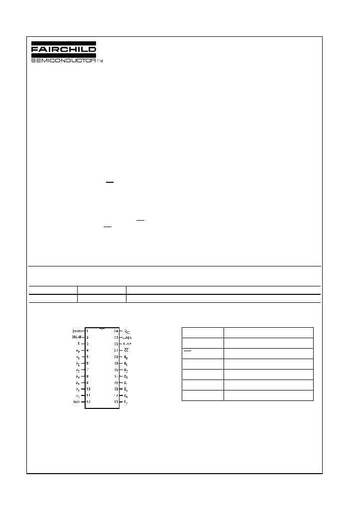
Connection Diagram
Pin Descriptions
Order Number
Package Number
Package Description
V320MTC
MTC24
24-Lead Thin Shrink Small Outline Package, JEDEC MO-153, 4.4mm Wide
Pin Names
Description
D
Direction A-to-B (High) B-to A (Low)
OE
Output Enable (Active LOW)
CLKAB/SELAB
A-to-B Clock/Select
CLKBA/SELBA
B-to-A Clock/Select
A0≠7
A Inputs/Outputs (TTL)
B0≠7
B Inputs/Outputs (TTL)
www.fairchildsemi.com
2
V320
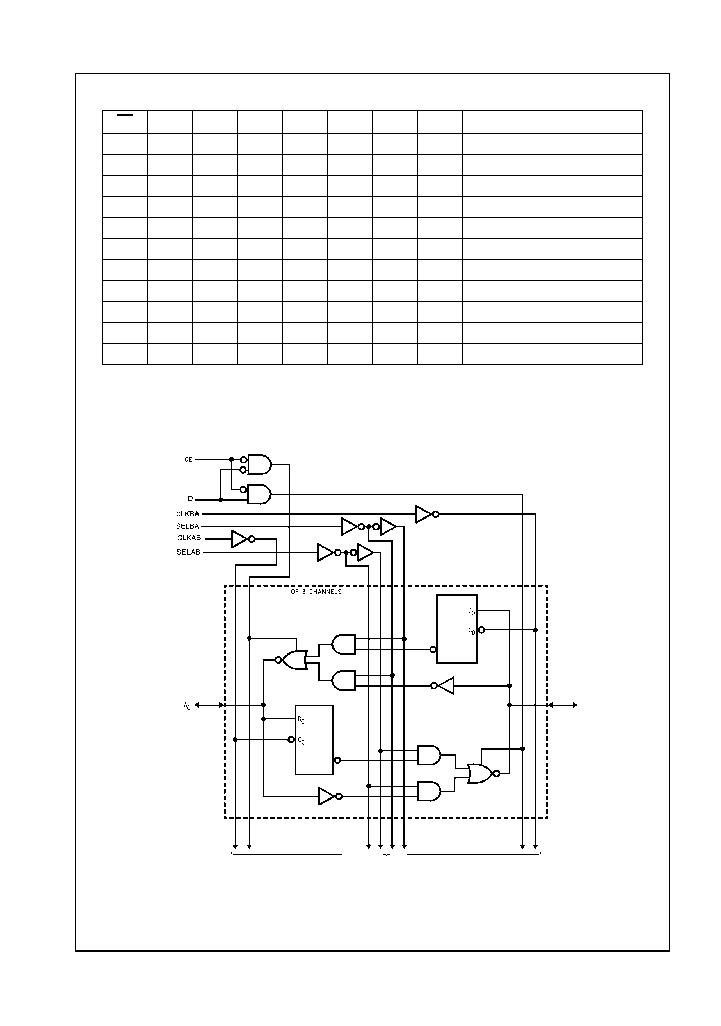
Functional Table
L
=
Low
H
=
High
LH
=
Low to High transition
X
=
Don't Care
Logic Diagram
Please note that this diagram is provided only for the understanding of logic operations and should not be used to estimate propagation delays.
OE
D
SELAB SELBA CLKAB CLKBA
A
0
≠A
7
B
0
≠B
7
Function
H
X
X
X
H or L
H or L
Isolation
H
X
X
X
LH
X
Input
Input
CLK A Data into A
H
X
X
X
X
LH
CLK B Data into A Reg.
L
H
L
X
X
X
A to B ≠ Transparent
L
H
L
X
LH
X
CLK A Data into A Reg.
L
H
H
X
H or L
X
Input
Output
A Reg. to B (Storage)
L
H
H
X
LH
X
CLK A Data into A Reg. and B output
L
L
X
L
X
X
B to A ≠ Transparent
L
L
X
L
X
LH
CLK B Data into B Reg.
L
L
X
H
X
H or L
Output
Input
B Reg. to A (Storage)
L
L
X
H
X
LH
CLK B Data into B Reg.and A output

3
www.fairchildsemi.com
V32
0
Absolute Maximum Ratings
(Note 1)
Recommended Operating
Conditions
Note 1: Absolute maximum ratings are values beyond which the device
may be damaged or have its useful life impaired. Functional operation
under these conditions is not implied.
Note 2: Either voltage limit or current limit is sufficient to protect inputs.
DC Electrical Characteristics (4.5V
<
V
CC
5.5V)
Over Recommended Operating Free-Air Temperature Range (Unless Otherwise Noted)
Note 3: Extended Characteristics (4.95
>
V
CC
>
5.05, T
=
25
∞
C
±
20
∞
C)
DC Input Voltage (V
I
)
-
0.5V to
+
7.0V
DC Output Voltage (V
O
)
Outputs 3-STATE
-
0.5V to
+
7.0V
Outputs Active (Note 2)
-
0.5V to V
CC
+
0.5V
DC Output Sink Current into
A-port/B-port I
OL
64 mA
DC Output Source Current from
A-port/B-port I
OH
-
32 mA
DC Input Diode Current (I
IK
)
V
I
<
0
V
-
30 mA to
+
5.0 mA
ESD Rating typical
>
2000V
Storage temperature (T
STG
)
-
65
∞
C to
+
15
∞
C
Max I
OL
(Current Applied to a
LOW Output)
2 X I
OL
Spec.
Supply Voltage V
CC
Operating V
CC
4.5V to 5.5V
Minimum Input Edge Rate
Data Input
50 mV/ns
Enable
20 mV/ns
Clock
100 mV/ns
Operating Temperature (T
A
)
-
40
∞
C to
+
85
∞
C
Symbol
Parameter
V
CC
(V)
Min
Typ
Max
Units
Conditions
V
IH
B-Port/A-Port HIGH Level Input Voltage
4.5≠5.5
2.0
V
Recognized HIGH Signal
4.95≠5.05
1.8
(Note 3)
V
IL
B-Port/A-Port LOW Level Input Voltage
4.5≠5.5
0.8
V
Recognized LOW Signal
4.95≠5.05
1.2
(Note 3)
V
OH
B-Port/A-Port HIGH Level Output Voltage
4.5
2.5
V
-
3 mA
4.5
2.0
-
32 mA
I
OH
B-Port/A-Port High Level Output Current Drive
4.5
-
32
mA
V
OH
=
2.0V
V
OL
B-Port/A-Port LOW Level Output Voltage
4.5
0.55
V
64 mA
I
OL
B-Port/A-Port Low Level Output Current Drive
(Sink)
4.5
64
mA
V
OL
=
0.55V
I
OS
B-Port/A-Port Short Circuit Current
5.5
-
100
-
275
mA
V
OUT
=
0.0V
I
OFF
A-Port and
Control Pins
Power-OFF Leakage Current
0.0
100uA
uA
V
OUT
=
5.5V, All Others
GND
I
CCH
B-Port/A-Port Quiescent Power Supply Current
5.5
250
uA
All Outputs HIGH
I
CCI
B-Port/A-Port B-Port/A-Port
5.5
30
mA
All Outputs LOW
I
CCZ
B-Port/A-Port 3-STATE Power Supply Current
5.5
50
uA
All Outputs 3-STATE
www.fairchildsemi.com
4
V320
Capacitance and Dynamic Switching Characteristics
Over Recommended Operating Free-Air Temperature Range (Unless Otherwise Noted)
AC Operating Requirements
Over recommended ranges of supply voltage and operating free-air temperature
Note 4: C
L
=
50 pF
Symbol
Parameter
Min
Typ
Max
Units
Conditions
T
A
=
25
∞
C
C
IN
Input Capacitance (Control Pin)
5
pF
V
CC
=
5.0V V
I
=
V
CC
or 0
C
I/O
Output Capacitance (A and B ports)
11
pF
V
CC
=
5.0V V
I
=
V
CC
or 0
Output Switching Noise (Ground Bounce)
V
OLP
Quiet Output Dynamic Peak V
OL
0.8
V
V
CC
=
5.0V, T
=
25
∞
C
V
OLV
Quiet Output Dynamic Valley V
OL
-
1.2
V
C
L
=
50 pF
V
OHV
Quiet Output Dynamic Valley V
OH
2.5
V
Input Noise Immunity (Dynamic Threshold)
V
IHD
High Level Threshold Movement
2.2
V
V
CC
=
5.0V, T
=
25
∞
C
V
ILD
Low Level Threshold Movement
0.5
V
C
L
=
50 pF
Symbol
Min
Typ
Max
Units
f
CLOCK
Max Clock Frequency
200 (Note 4)
MHz
t
WIDTH
Pulse Duration
HIGH or LOW
3.0
ns
t
SU
Setup Time
Bus to CLKAB/CLKBA
1.5
ns
t
HOLD
Hold Time
Bus to CLKAB/CLKBA
1.0
ns
5
www.fairchildsemi.com
V32
0
AC Electrical Characteristics
(
-
40
∞
C to 85
∞
C, V
CC
=
4.5V to 5.5V) 1 Output Switching
Note 5: 3-STATE delays are dominated by the RC Network (500
/ 250 pF, or 500
/ 500 pF) on the output and thus have been excluded from this
datasheet.
Symbol
From
(Input)
Mode
To
(Output)
Min
Typ
Max
Units
Output Load: C
L
=
50 pF, R
L
=
500
, 1 Output Switching
t
PLH
, t
PHL
CLKAB/CLKBA
Register
Bus A or B
1.7
5.6
ns
t
PLH
, t
PHL
Bus A or B
Transparent
Bus A or B
1.5
4.8
ns
t
PLH
, t
PHL
SELAB/SELBA
Select Bus
Bus A or B
1.5
5.9
ns
t
PLZ
, t
PHZ
OE
Output Disable
Bus A or B
1.5
6.0
ns
t
PZH
, t
PZL
OE
Output Enable
Bus A or B
1.5
6.3
ns
t
PLZ
, t
PHZ
Direction (D)
Dir. Disable
Bus A or B
1.5
6.0
ns
t
PZH
, t
PZL
Direction (D)
Dir. Enable
Bus A or B
1.5
6.3
ns
t
RISE
Transition Time, Outputs (1V to 2V)
0.3
1.2
ns
t
FALL
Transition Time, Outputs (1V to 2V)
0.3
1.4
ns
Output Load: C
L
=
250 pF, R
L
=
500
, 1 Output Switching
t
PLH
, t
PHL
CLKAB/CLKBA
Register
Bus A or B
2.0
7.5
ns
t
PLH
, t
PHL
Bus A or B
Transparent
Bus A or B
2.0
7.0
ns
t
PLH
, t
PHL
SELAB/SELBA
Select Bus
Bus A or B
2.0
7.5
ns
t
PLZ
, t
PHZ
OE
Output Disable
Bus A or B
(Note 5)
(Note 5)
ns
t
PZH
, t
PZL
OE
Output Enable
Bus A or B
2.0
8.0
ns
t
PLZ
, t
PHZ
Direction (D)
Dir. Disable
Bus A or B
(Note 5)
(Note 5)
ns
t
PZH
, t
PZL
Direction (D)
Dir. Enable
Bus A or B
2.0
8.3
ns
t
RISE
Transition Time, Outputs (1V to 2V)
1.7
3.9
ns
t
FALL
Transition Time, Outputs (1V to 2V)
0.8
3.1
ns
Output Load: C
L
=
500 pF, R
L
=
500
, Output Switching
t
PLH
t
PHL
CLKAB/CLKBA
Register
Bus A or B
3.0
12.2
ns
t
PLH
t
PHL
Bus A or B
Transparent
Bus A or B
3.0
11.6
ns
t
PLH
t
PHL
SELAB/SELBA
Select Bus
Bus A or B
3.0
12.4
ns
t
PLZ
, t
PHZ
OE
Output Disable
Bus A or B
(Note 5)
(Note 5)
ns
t
PZH
, t
PZL
OE
Output Enable
Bus A or B
3.0
12.6
ns
t
PLZ
, t
PHZ
Direction (D)
Dir. Disable
Bus A or B
(Note 5)
(Note 5)
ns
t
PZH
, t
PZL
Direction (D)
Dir. Enable
Bus A or B
6.3
13.2
ns
t
RISE
Transition Time, Outputs (1V to 2V)
3.5
7.2
ns
t
FALL
Transition Time, Outputs (1V to 2V)
1.4
5.1
ns