 | ÐлекÑÑоннÑй компоненÑ: X5563 | СкаÑаÑÑ:  PDF PDF  ZIP ZIP |
/home/web/doc/html/fairchild/206585

REV 1.0 6/27/00
Characteristics subject to change without notice.
1 of 22
www.xicor.com
Preliminary Information
256K
X55621
Dual Voltage Monitor with Integrated System Battery Switch and EEPROM
FEATURES
· Dual voltage monitoring
· System battery switch-over circuitry
· Early warning low V
CC
fail indicator
· Separate watchdog timer outputs
· Selectable watchdog timer
--(0.15s, 0.4s, 0.8s, off)
· Low V
CC
(V1MON) and V2MON detection and
reset assertion
--Four standard reset threshold voltages
--Re-program V1
TRIP
and V2
TRIP
reset threshold
voltage using special programming sequence
--Reset signal valid to V
CC
= 1V
· Long battery life with low power consumption
--<50µA max standby current, watchdog on
--<30µA max standby current, watchdog off
--<1.5mA max active current during read
· 256Kbits of EEPROM
· Built-in inadvertent write protection
--Power-up/power-down protection circuitry
--Protect 0, 1/4, 1/2 or all of EEPROM array with
programmable Block Lock
TM
protection
--In circuit programmable ROM mode
· 10MHz SPI interface modes (0,0 & 1,1)
· Minimize EEPROM programming time
--64-byte page write mode
--Self-timed write cycle
--5ms write cycle time (typical)
· 2.7V to 5.5V power supply operation
· Available packages
--20-lead TSSOP
DESCRIPTION
This device combines power-on reset control, battery
switch circuit, watchdog timer, supply voltage supervi-
sion, secondary voltage supervision, block lock
protect
and serial EEPROM in one package. This combination
lowers system cost, reduces board space require-
ments, and increases reliability.
Applying power to the device activates the power on
reset circuit which holds RESET active for a period of
time. This allows the power supply and oscillator to sta-
bilize before the processor can execute code.
A system battery switch circuit compares V
CC
(V1MON)
with V
BATT
input and connects V
OUT
to whichever is
higher. This provides voltage to external SRAM or
other circuits in the event of main power failure. The
X55621 can drive 50mA from V
CC
and 250µA from
V
BATT
. The device switches to V
BATT
when V
CC
drops
below the low V
CC
voltage threshold and V
BATT
.
The Watchdog Timer provides an independent
protection mechanism for microcontrollers. When the
micro-controller fails to restart a timer within a select-
able time out interval, the device activates the WDO
signal. The user selects the interval from three preset
values. Once selected, the interval does not change,
even after cycling the power.
The device's low V
CC
detection circuitry protects the
user's system from low voltage conditions, resetting the
system when V
CC
(V1MON) falls below the minimum
V
CC
trip point (V
TRIP
). RESET is asserted until V
CC
returns to proper operating level and stabilizes. A second
voltage monitor circuit tracks the unregulated supply or
monitors a second power supply voltage to provide a
power fail warning. Xicor's unique circuits allow the
threshold for either voltage monitor to be reprogrammed
to meet special needs or to fine-tune the threshold for
applications requiring higher precision.
X55621 Preliminary Information
Characteristics subject to change without notice.
2 of 22
REV 1.0 6/27/00
www.xicor.com
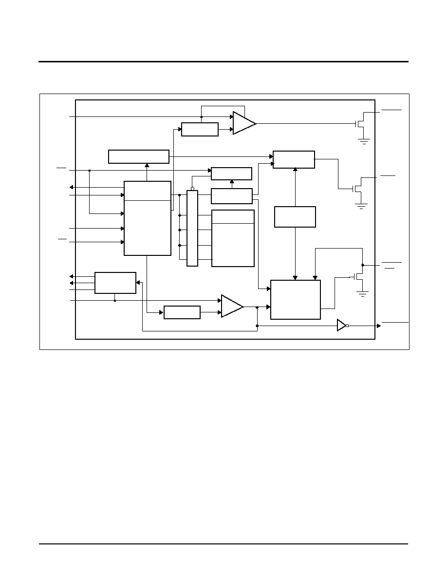
BLOCK DIAGRAM
Watchdog
Timer Reset
Data
Register
Command
Decode, Test
& Control
Logic
SI
SO
SCK
CS
V
CC
Reset &
Watchdog
Timebase
Power On,
Generation
V
CC
Monitor
+
-
WDO
Reset
Low Voltage
Status
Register
Protect Logic
EEPROM Array
Watchdog Transition
Detector
WP
512 X 512
X-Decoder
V1
TRIP
Logic
V2 Monitor
+
-
V2
TRIP
Logic
System
Switch
RESET
LOWLINE
V2FAIL
V2MON
V
BATT
V
OUT
BATT-ON
(V1MON)
Manual and
\ MR
Battery
X55621 Preliminary Information
Characteristics subject to change without notice.
3 of 22
REV 1.0 6/27/00
www.xicor.com
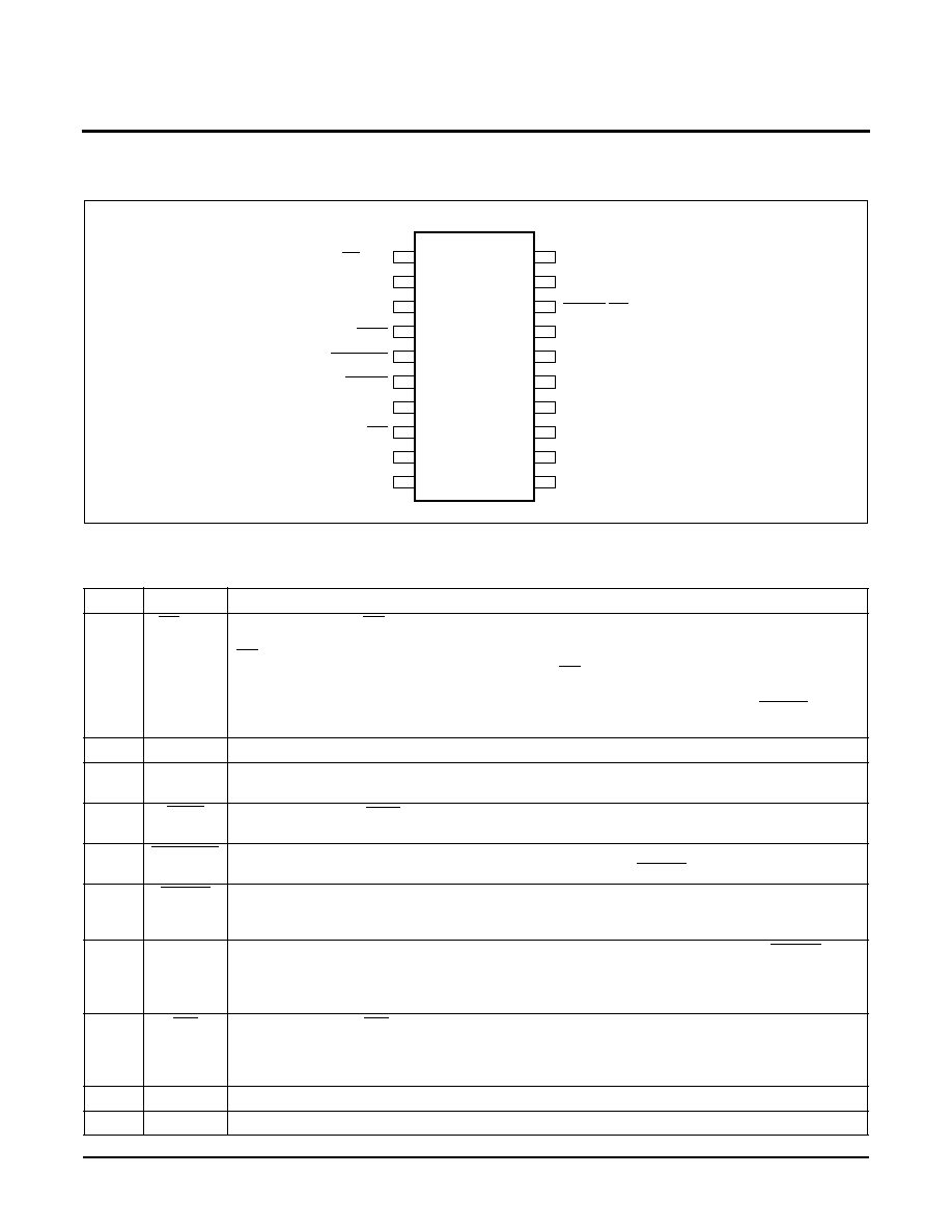
PIN CONFIGURATION
PIN DESCRIPTION
Pin
Name
Function
1
CS/WDI
Chip Select Input.
CS HIGH, deselects the device and the SO output pin is at a high impedance
state. Unless a nonvolatile write cycle is underway, the device will be in the standby power mode.
CS LOW enables the device, placing it in the active power mode. Prior to the start of any opera-
tion after power up, a HIGH to LOW transition on CS is required.
Watchdog Input.
A HIGH to LOW transition on the WDI pin restarts the Watchdog timer. The
absence of a HIGH to LOW transition within the watchdog time out period results in RESET going
active.
2
NC
No internal connections
3
SO
Serial Output.
SO is a push/pull serial data output pin. A read cycle shifts data out on this pin. The
falling edge of the serial clock (SCK) clocks the data out.
4
WDO
Watchdog Output
.
WDO
is an active Low, open drain output which goes active whenever the
watchdog timer goes active.
5
LOWLINE
Early Low V
CC
Detect
.
This CMOS output signal goes LOW when V
CC
< V1
TRIP
and returns
HIGH when V
CC
> V1
TRIP
. This pin goes LOW 250ns before RESET pin.
6
V2FAIL
V2 Voltage Fail Output.
This open drain output goes LOW when V2MON is less than V2
TRIP
and goes HIGH when V2MON exceeds V2
TRIP
. There is no power up reset delay circuitry on this
pin. This circuit works independently from the Low V
CC
reset and battery switch circuits.
7
V2MON
V2 Voltage Monitor Input.
When the V2MON input is less than the V2
TRIP
voltage, V2FAIL goes
LOW. This input can monitor an unregulated power supply with an external resistor divider or can
monitor a second power supply with no external components. Connect V2MON to V
SS
or V
CC
when not used.
8
WP
Write Protect.
The WP pin works in conjunction with a nonvolatile WPEN bit to "lock" the setting
of the Watchdog Timer control and the memory write protect bits. This pin is also used as the test
mode enable pin where the high voltage will be applied. Thus the layout for the input is different
to allow for higher punch thru.
9
NC
No internal connections
10
V
SS
Ground
20-Pin TSSOP
CS/WDI
SO
NC
1
2
3
4
RESET/MR
V
CC
(V1MON)
BATT-ON
V
OUT
5
6
7
8
9
10
20
19
18
17
16
15
14
13
12
11
WDO
LOWLINE
V2FAIL
V2MON
WP
NC
VSS
V
BATT
SCK
NC
NC
SI
NC

X55621 Preliminary Information
Characteristics subject to change without notice.
4 of 22
REV 1.0 6/27/00
www.xicor.com
11
SI
Serial Input.
SI is a serial data input pin. Input all opcodes, byte addresses, and memory data on
this pin. The rising edge of the serial clock (SCK) latches the input data. Send all opcodes (Table 1),
addresses and data MSB first.
12
NC
No internal connections
13
NC
No internal connections
14
SCK
Serial Clock.
The Serial Clock controls the serial bus timing for data input and output. The rising
edge of SCK latches in the opcode, address, or data bits present on the SI pin. The falling edge of
SCK changes the data output on the SO pin.
15
V
BATT
Battery Supply Voltage.
This input provides a backup supply in the event of a failure of the pri-
mary V
CC
voltage. The V
BATT
voltage typically provides the supply voltage necessary to main-
tain the contents of SRAM and also powers the internal logic to "stay awake."
16
V
OUT
Output Voltage.
V
OUT
= V
CC
if V
CC
> V1
TRIP
. IF V
CC
< V1
TRIP
, then V
OUT
= V
CC
if V
CC
>
V
BATT
+ 0.03, or V
OUT
= V
BATT
if V
CC
< V
BATT
0.03.
Note:
There is hysteresis around V
BATT
± 0.03V point to avoid oscillation at or near the switcho-
ver voltage. A capacitance of 0.1µF must be connected to Vout to ensure stability.
17
BATT-ON
Battery On.
This CMOS output goes HIGH when the V
OUT
switches to V
BATT
and goes LOW
when V
OUT
switches to V
CC
. It is used to drive an external PNP pass transistor when V
CC
= V
OUT
and current requirements are greater than 50mA.
The purpose of this output is to drive an external transistor to get higher operating currents when
the V
CC
supply is fully functional. In the event of a V
CC
failure, the battery voltage is applied to
the V
OUT
pin and the external transistor is turned off. In this "backup condition," the battery only
needs to supply enough voltage and current to keep SRAM devices from losing their data-there
is no communication at this time.
18
RESET
/MR
RESET Output
.
This is an active LOW, open drain output which goes active whenever V
CC
falls
below the minimum V
CC
sense level. Then communication to the device is interrupted. It will remain
active until V
CC
rises above the minimum V
CC
sense level for 150ms. RESET also goes active on
power up and remains active for 150ms after the power supply stabilizes.
19
NC
No internal connections
20
V
CC
(V1MON)
Supply Voltage
V1 Voltage Monitor Input.
When the V1MON input is less than the V1
TRIP
voltage, RESET and
RESET goes ACTIVE.
PIN DESCRIPTION (CONTINUED)
Pin
Name
Function
X55621 Preliminary Information
Characteristics subject to change without notice.
5 of 22
REV 1.0 6/27/00
www.xicor.com
PRINCIPLES OF OPERATION
Power On Reset
Application of power to the X55621 activates a Power
On Reset Circuit. This circuit goes active at about 1V
and pulls the RESET pin active. This signal prevents the
system microprocessor from starting to operate with
insufficient voltage or prior to stabilization of the oscilla-
tor. When Vcc exceeds the device V1
TRIP
value for
150ms (nominal) the circuit releases RESET, allowing
the processor to begin executing code.
Low V
CC
(V1MON) Voltage Monitoring
During operation, the X55621 monitors the V
CC
level
and asserts RESET if supply voltage falls below a preset
minimum V1
TRIP
. During this time the communication
to the device is interrupted. The RESET signal also pre-
vents the microprocessor from operating in a power fail
or brownout condition. The RESET signal remains
active until the voltage drops below 1V. These also
remain active until V
CC
returns and exceeds V1
TRIP
for
150ms.
Low V2MON Voltage Monitoring
The X55621 also monitors a second voltage level and
asserts V2FAIL if the voltage falls below a preset mini-
mum V2
TRIP
. The V2FAIL signal is either ORed with
RESET to prevent the microprocessor from operating
in a power fail or brownout condition or used to inter-
rupt the microprocessor with notification of an impend-
ing power failure. The V2FAIL signal remains active
until the V2MON drops below 1V (V2MON falling). It
also remains active until V2MON returns and exceeds
V2
TRIP
by 0.03V.
The V2MON voltage sensor is completely separate
from the operation of the low V
CC
sense, and is inde-
pendent of V
CC
supply.
Figure 1. Two Uses of Dual Voltage Monitoring
X55621
X55621
V
OUT
V
OUT
5V
Reg
5V
Reg
5V
Reg
V
CC
V
CC
RESET
RESET
V2MON
V2MON
V2FAIL
V2FAIL
System
Reset
Unregulated
Supply
System
Reset
System
Interrupt
R
R
Unregulated
Supply
Resistors selected so 3V appears on V2MON when
Unregulated supply reaches 6V.
Notice: No external components required to monitor
two voltages.
V2MON
Watchdog Timer
The Watchdog Timer circuit monitors the microproces-
sor activity by monitoring the CS pin. The microproces-
sor must toggle the CS pin HIGH to LOW periodically
prior to the expiration of the watchdog time out period
to prevent the WDO signal going active. The state of
two nonvolatile control bits in the Status Register
determines the watchdog timer period. The micropro-
cessor can change these watchdog bits by writing to
the status register.
The Watchdog Timer oscillator stops when in battery
backup mode. It re-starts when V
CC
returns.
System Battery Switch
As long as V
CC
exceeds the low voltage detect thresh-
old V1
TRIP
, V
OUT
is connected to V
CC
through a 5 Ohm
(typical) switch. When the V
CC
has fallen below V
TRIP
,
then V
CC
is applied to V
OUT
if V
CC
is or equal to or
greater than V
BATT
0.03V. When V
CC
drops to less
than V
BATT
0.03V, then V
OUT
is connected to V
BATT
through an 80 Ohm (typical) switch. V
OUT
typically
supplies the system static RAM voltage, so the
switchover circuit operates to protect the contents of
the static RAM during a power failure. Typically, when
V
CC
has failed, the SRAMs go into a lower power state
and draw much less current than in their active mode.
When V
CC
returns, V
OUT
switches back to V
CC
when
V
CC
exceeds V
BATT
+ 0.03V. There is a 60mV hystere-
sis around this battery switch threshold to prevent
oscillations between supplies.
While V
CC
is connected to V
OUT
the BATT-ON pin is
pulled LOW. The signal can drive an external PNP
transistor to provide additional current to the external
circuits during normal operation.