 | ÐлекÑÑоннÑй компоненÑ: X9430W | СкаÑаÑÑ:  PDF PDF  ZIP ZIP |
X9430.fm
REV 1.0 6/20/00
Characteristics subject to change without notice.
1 of 21
www.xicor.com
Preliminary Information
Programmable Analog
X9430
Dual Digitally Controlled Potentiometer (XDCP
TM
) with Operational Amplifier
FEATURES
· Two CMOS voltage operational amplifiers
· Two digitally controlled potentiometers
· Can be combined or used separately
· Amplifiers
--Low voltage operation
--V+/V- = ±2.7V to ±5.5V
--Rail-to-rail CMOS performance
--1MHz gain bandwidth product
· Digitally controlled potentiometer
--Dual 64 tap potentiometers
--R
total
= 10k
--SPI serial interface
--V
CC
= 2.7V to 5.5V
DESCRIPTION
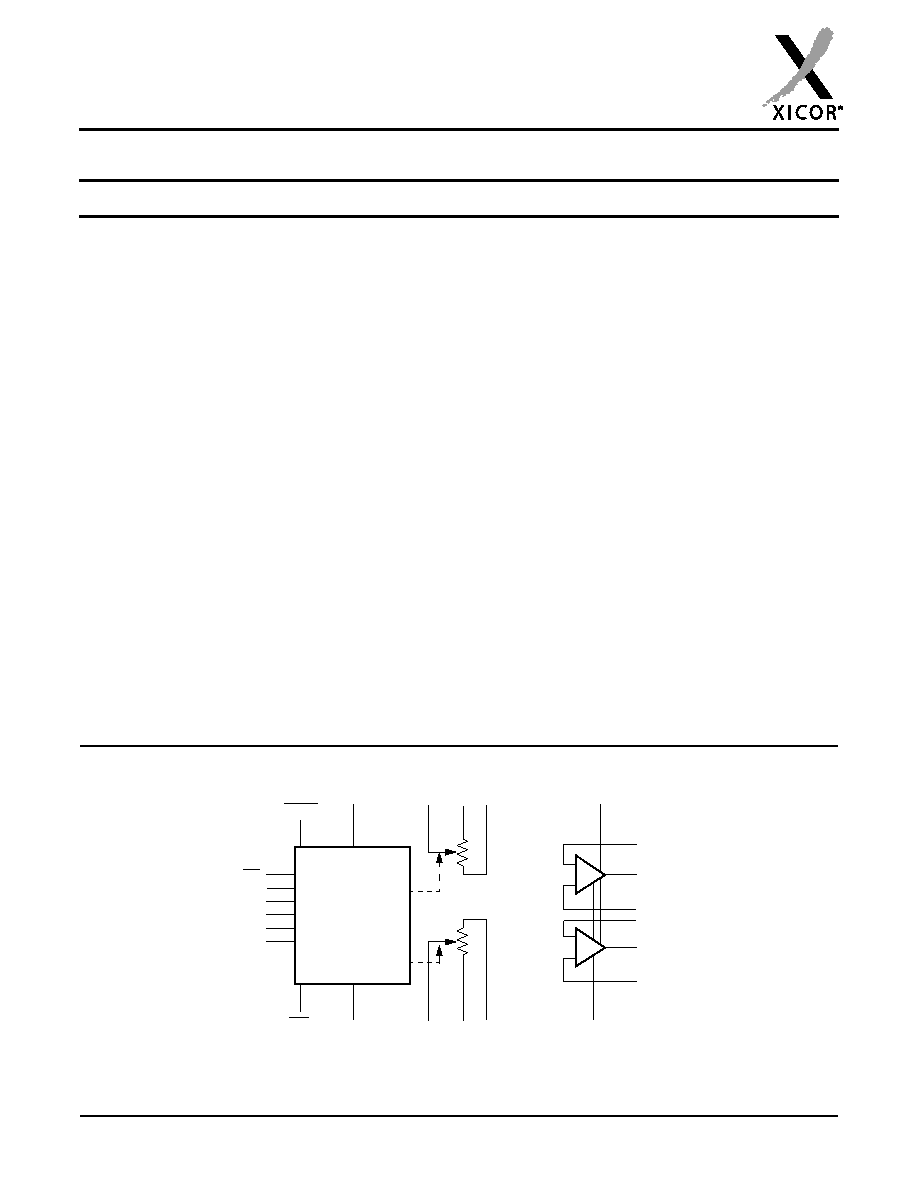
The X9430 is a monolithic CMOS IC that incorporates
two operational amplifiers and two nonvolatile digitally
controlled potentiometers. The amplifiers are CMOS
differential input voltage operational amplifiers with
near rail-to-rail outputs. All pins for the two amplifiers
are brought out of the package to allow combining
them with the potentiometers or using them as com-
plete stand-alone amplifiers.
The digitally controlled potentiometers consist of a
series string of 63 polycrystalline resistors that behave
as standard integrated circuit resistors. The SPI serial
port, common to both pots, allows the user to program
the connection of the wiper output to any of the resistor
nodes in the series string. The wiper position is saved
in the on board E2 memory to allow for nonvolatile res-
toration of the wiper position.
A wide variety of applications can be implemented
using the potentiometers and the amplifiers. A typical
application is to implement the amplifier as a wiper
buffer in circuits that use the potentiometer as a voltage
reference. The potentiometer can also be combined
with the amplifier yielding a digitally programmable gain
amplifier or programmable current source.
BLOCK DIAGRAM
V
OUT1
Control and
CS
SCK
SO
SI
A1
A0
+
Memory
V
CC
V
NI0
V+
V
R
W0
V
SS
V
OUT0
+
V
NI1
V
INV1
V
INV0
R
H0
R
L0
R
W1
R
L1
R
H1
WCR1
WCR0
WP
HOLD

X9430 Preliminary Information
Characteristics subject to change without notice.
2 of 21
REV 1.0 6/20/00
www.xicor.com
PIN DESCRIPTIONS
Host Interface Pins
Serial Output (SO)
SO is a push/pull serial data output pin. During a read
cycle, data is shifted out on this pin. Data is clocked
out by the falling edge of the serial clock.
Serial Input (SI)
SI is the serial data input pin. All opcodes, byte
addresses and data to be written to the device are
input on this pin. Data is latched by the rising edge of
the serial clock.
Serial Clock (SCK)
The SCK input is used to clock data into and out of the
X9430.
Chip Select (CS)
When CS is HIGH, the X9430 is deselected and the
SO pin is at high impedance, and (unless an internal
write cycle is underway) the device will be in the
standby state. CS LOW enables the X9430, placing it
in the active power mode. It should be noted that after
a power-up, a HIGH to LOW transition on CS is
required prior to the start of any operation.
Hardware Write Protect Input WP
The WP pin when low prevents nonvolatile writes to
the wiper counter register.
Hold (HOLD)
HOLD is used in conjunction with the CS pin to select
the device. Once the part is selected and a serial
sequence is underway, HOLD may be used to pause
the serial communication with the controller without
resetting the serial sequence. To pause, HOLD must
be brought LOW while SCK is LOW. To resume com-
munication, HOLD is brought HIGH, again while SCK
is LOW. If the pause feature is not used, HOLD should
be held HIGH at all times.
Device Address (A
0
A
1
)
The address inputs are used to set the least significant
2 bits of the 8-bit slave address. A match in the slave
address serial data stream must be made with the
address input in order to initiate communication with
the X9430. A maximum of 4 devices may occupy the
SPI serial bus.
Potentiometer Pins
1
R
H
(R
H0
R
H1
), R
L
(R
L0
R
L1
)
The R
H
and R
L
inputs are equivalent to the terminal
connections on either end of a mechanical potentiom-
eter.
R
W
(R
W0
R
W1
)
The wiper output is equivalent to the wiper output of a
mechanical potentiometer.
Amplifier and Device Pins
Amplifier Input Voltage V
NI
(0,1) and V
INV
(0,1)
V
NI
and V
INV
are inputs to the noninverting (+) and
inverting (-) inputs of the operational amplifiers.
Amplifier Output Voltage V
OUT
(0,1)
V
OUT
is the voltage output pin of the operational ampli-
fier.
Analog Supplies V+, V-
The Analog Supplies V+, V- are the supply voltages
for the XDCP analog section and the operational
amplifiers.
System Supply V
CC
and Ground V
SS
The system supply V
CC
and its reference V
SS
is used
to bias the interface and control circuits.
1.
Alternate designations for R
H
, R
L
, R
W
are V
H
, V
L
, V
W
X9430
Preliminary Information
Characteristics subject to change without notice.
3 of 21
REV 1.0 6/20/00
www.xicor.com
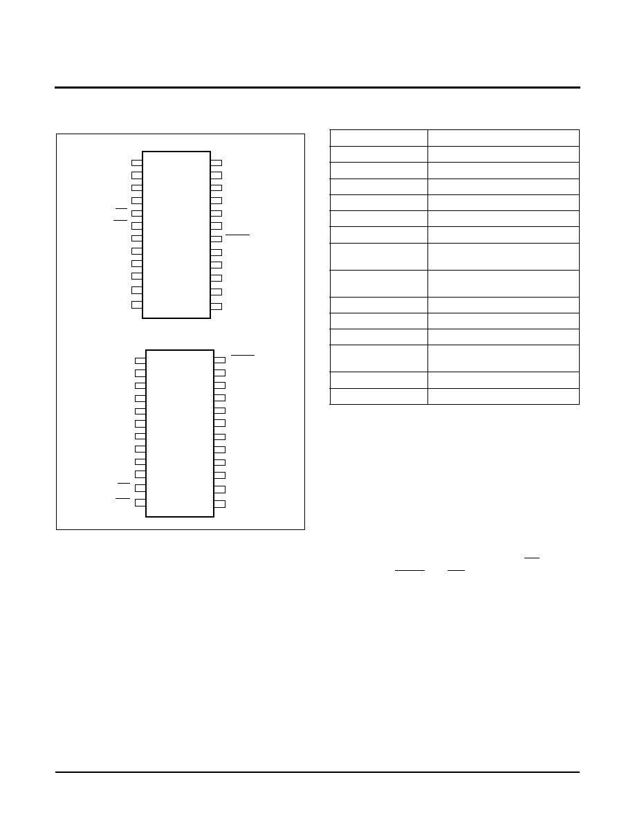
PIN CONFIGURATION
PIN NAMES
PRINCIPLES OF OPERATION
The X9430 is an integrated microcircuit incorporating two
digitally controlled potentiometers, two operational
amplifiers and their associated registers and counters;
and the serial interface logic providing direct communica-
tion between the host and the digitally controlled
potentiometers.
Serial Interface
The X9430 supports the SPI interface hardware con-
ventions. The device is accessed via the SI input with
data clocked in on the rising edge of SCK. CS must be
LOW and the HOLD and WP pins must be HIGH dur-
ing the entire operation.
V
CC
R
L0
R
H0
WP
A1
1
2
3
4
5
6
7
8
9
10
24
23
22
21
20
19
18
17
16
15
V+
V
OUT0
V
NI0
V
INV0
A0
S0
HOLD
SCK
V
INV1
V
NI1
SOIC
X9430
V
SS
R
W0
14
13
11
12
CS
R
L1
R
H1
R
W1
V
OUT1
V-
SI
V-
V
INV0
V
NI0
HOLD
SO
SCK
1
2
3
4
5
6
7
8
9
10
24
23
22
21
20
19
18
17
16
CS
V
CC
R
W0
TSSOP
X9430
V+
V
OUT0
11
12
A
0
V
OUT1
V
NI1
V
INV1
R
L0
R
H0
V
SS
R
W1
R
H1
R
L1
A
1
SI
WP
15
14
13
Symbol
Description
SCK
Serial Clock
SI
Serial Input
SO
Serial Output
A0-A1
Device Address
CS
Chip Select
HOLD
Hold
R
H0
R
H1
, R
L0
R
L1
Potentiometers (terminal
equivalent)
R
W0
R
W1
Potentiometers (wiper
equivalent)
V
NI(0,1)
, V
INV(0,1)
Amplifier Input Voltages
V
OUT0,
V
OUT1
Amplifier Outputs
WP
Hardware Write Protection
V+,V-
Analog and Voltage Amplifier
Supplies
V
CC
System/Digital Supply Voltage
V
SS
System Ground
X9430
Preliminary Information
Characteristics subject to change without notice.
4 of 21
REV 1.0 6/20/00
www.xicor.com
Potentiometer/Array Description
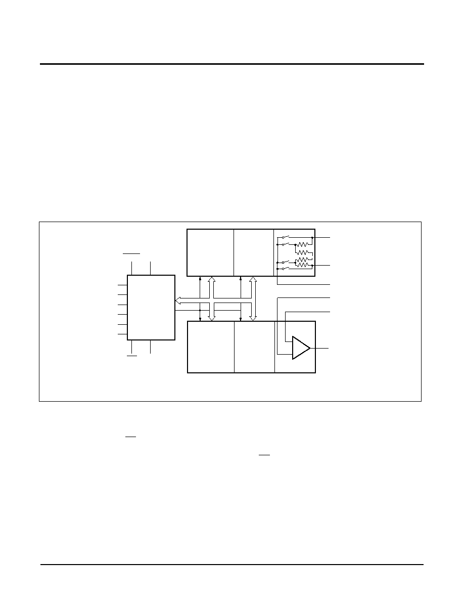
The X9430 is comprised of two resistor arrays and two
operational amplifiers. Each array contains 63 discrete
resistive segments that are connected in series. The
physical ends of each array are equivalent to the fixed
terminals of a mechanical potentiometer (R
H
and R
L
).
At both ends of each array and between each resistor
segment is a CMOS switch connected to the wiper
(R
W
) output. Within each individual array only one
switch may be turned on at a time. These switches are
controlled by a volatile wiper counter register (WCR).
The six bits of the WCR are decoded to select, and
enable, one of sixty-four switches.
The WCR may be written directly, or it can be changed
by transferring the contents of one of four associated
data registers into the WCR. These data registers and
the WCR can be read and written by the host system.
Operational Amplifier
The voltage operational amplifiers are CMOS rail-to-rail
output general purpose amplifiers. They are designed
to operate from dual (±) power supplies. The amplifiers
may be configured like any standard amplifier. All pins
are externally available to allow connection with the
potentiometers or as stand alone amplifiers.
Detailed Block Diagram
V
OUT (0,1)
(DR0-DR3)
0,1
Control and
CS
SCK
SO
SI
A1
A0
V
H (0,1)
V
L (0,1)
WP
V
W (0,1)
V
N (0,1)
+
WCR
0,1
(DR0-DR3)
0,1
V
INV (0,1)
V
SS
V
CC
HOLD
Memory
WCR0
WCR1
(One of 2 Circuits)
Write in Process
The contents of the data registers are saved to nonvol-
atile memory when the CS pin goes from LOW to
HIGH after a complete write sequence is received by
the device. The progress of this internal write opera-
tion can be monitored by a write in process bit (WIP).
The WIP bit is read with a read status command.
INSTRUCTIONS AND PROGRAMMING
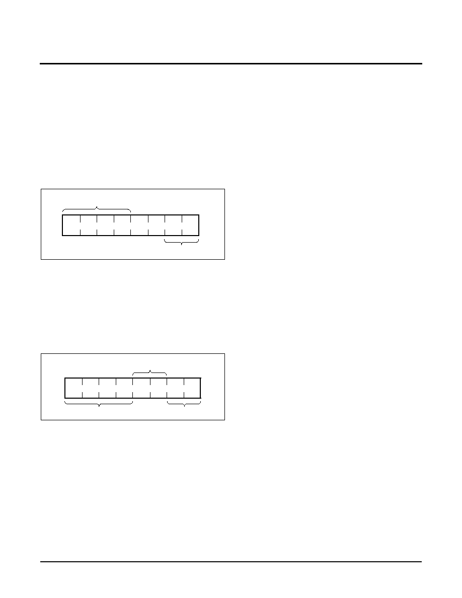
Identification (ID) Byte
The first byte sent to the X9430 from the host, follow-
ing a CS going HIGH to LOW, is called the identifica-
tion byte. The most significant four bits of the slave
address are a device type identifier, for the X9430 this
is fixed as 0101[B] (refer to Figure 1).
X9430
Preliminary Information
Characteristics subject to change without notice.
5 of 21
REV 1.0 6/20/00
www.xicor.com
The two least significant bits in the ID byte select one of
four devices on the bus. The physical device address is
defined by the state of the A
0
-A
1
input pins. The X9430
compares the serial data stream with the address input
state; a successful compare of both address bits is
required for the X9430 to successfully continue the
command sequence. The A
0
A
1
inputs can be actively
driven by CMOS input signals or tied to V
CC
or V
SS
.
The remaining two bits in the slave byte must be set to 0.
Figure 1. Identification Byte Format
Instruction Byte
The next byte sent to the X9430 contains the instruc-
tion and register pointer information. The four most sig-
nificant bits are the instruction. The next four bits point
to one of the WCRs of the two pots, and when applica-
ble, they point to one of four associated data registers.
The format is shown below in Figure 2.
Figure 2. Instruction Byte Format
The four high order bits of the instruction byte specify
the operation. The next two bits (R
1
and R
0
) select one
of the four registers that is to be acted upon when a
register oriented instruction is issued. The last bit (P
0
)
selects which one of the two potentiometers is to be
affected by the instruction.
Four of the ten instructions are two bytes in length and
end with the transmission of the instruction byte.
The basic sequence of the two byte instructions is illus-
trated in Figure 3. These two-byte instructions
exchange data between a wiper counter register and
one of the four data registers associated with each. A
transfer from a data register to a wiper counter register
is essentially a write to a static RAM. The response of
the wiper to this action will be delayed t
WRL
. A transfer
from the wiper counter register (current wiper position)
to a data register is a write to nonvolatile memory and
takes a minimum of t
WR
to complete. The transfer can
occur between one of the two potentiometers and one
of its associated registers; or it may occur globally,
wherein the transfer occurs between both of the poten-
tiometers and one of their associated registers.
Five instructions require a three-byte sequence to com-
plete. These instructions transfer data between the
host and the X9430; either between the host and one
of the data registers or directly between the host and
the Wiper Counter and Registers. These instructions
are: 1) Read Wiper Counter Register, read the current
wiper position of the selected pot 2) Write Wiper
Counter Register, i.e. change current wiper position of
the selected pot; 3) Read Data Register, read the con-
tents of the selected nonvolatile register; 4) Write Data
Register, write a new value to the selected data register;
5)Read Status, returns the contents of the WIP bit which
indicates if an internal write cycle is in progress.
The sequence of these operations is shown in Figure 4
and Figure 5.
The final command is Increment/Decrement. It is differ-
ent from the other commands, because it's length is
indeterminate. Once the command is issued, the mas-
ter can clock the selected wiper up and/or down in one
resistor segment steps; thereby, providing a fine tuning
capability to the host. For each SCK clock pulse (t
HIGH
)
while SI is HIGH, the selected wiper will move one
resistor segment towards the V
H
terminal. Similarly, for
each SCK clock pulse while SI is LOW, the selected
wiper will move one resistor segment towards the V
L
terminal. A detailed illustration of the sequence and
timing for this operation are shown in Figure 6 and
Figure 7.
1
0
0
0
0
A1
A0
Device Type
Identifier
Device Address
1
I1
I2
I3
I0
R1
R0
0
P0
WCR Select
Register
Select
Instructions