 | ÐлекÑÑоннÑй компоненÑ: X9440Y | СкаÑаÑÑ:  PDF PDF  ZIP ZIP |
X9440.fm
REV 1.0 2/27/01
Characteristics subject to change without notice.
1 of 22
www.xicor.com
X9440
Dual Digitally Controlled Potentiometer (XDCP
TM
) & Voltage Comparator
FEATURES
· Two digitally controlled potentiometers and two
voltage comparators in one package
· SPI serial interface
· Register oriented format
--Direct read/write wiper position
--Store as many as four positions per pot
· Fast response comparator
· Enable, latch, or shutdown comparator outputs
through the ACR
· Auto-recall of WCR and ACR data from R0
· Hardware write protection, WP
· Separate analog and digital/system supplies
· Direct write cell
--Endurance100,000 data changes per bit per
register
--Register data retention100 years
· 16-bytes of EEPROM memory
· Power saving feature and low noise
· Two 10K
or two 2.5K
potentiometers
· Resolution: 64 taps each pot
· 24-lead TSSOP and 24-Lead SOIC packages
DESCRIPTION
The X9440 integrates two non volatile digitally con-
trolled potentiometers (XDCP) and two voltage com-
parators on a CMOS monolithic microcircuit.
The X9440 contains two resistor arrays, each com-
posed of 63 resistive elements. Between each element
and at either end are tap points accessible to the wiper
elements. The position of the wiper element on the
array is controlled by the user through the SPI serial
bus interface.
Each potentiometer has an associated voltage com-
parator. The comparator compares the external input
voltage V
NI
with the wiper voltage V
W
and sets the out-
put voltage level to a logic high or low.
Each resistor array and comparator has associated
with it a wiper counter register (WCR), analog control
register (ACR), and eight 6 bit data registers that can
be directly written and read by the user. The contents
of the wiper counter register controls the position of
the wiper on the resistor array. The contents of the
analog control register controls the comparator and its
output. The potentiometer is programmed with a SPI
serial interface.
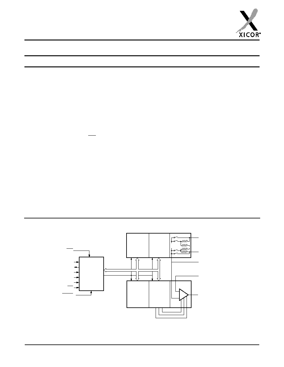
BLOCK DIAGRAM
V
OUT (0,1)
(R
0
-R
3
)
0,1
Interface
and
Control
Circuitry
SCK
S0
SI
A1
CS
HOLD
V
H (0,1)
V
L (0,1)
WP
V
W (0,1)
V
NI (0,1)
+
WCR
0,1
(R
0
-R
3
)
0,1
ACR
0,1
A0
Mixed Signal with SPI Interface

X9440
Characteristics subject to change without notice.
2 of 22
REV 1.0 2/27/01
www.xicor.com
PIN DESCRIPTIONS
Host Interface Pins
Serial Output (SO)
SO is a push/pull serial data output pin. During a read
cycle, data is shifted out on this pin. Data is clocked out
by the falling edge of the serial clock.
Serial Input (SI)
SI is the serial data input pin. All opcodes, byte
addresses and data to be written to the pots and pot
registers are input on this pin. Data is latched by the
rising edge of the serial clock.
Serial Clock (SCK)
The SCK input is used to clock data into and out of the
X9440.
Chip Select (CS)
When CS is HIGH, the X9440 is deselected and the
SO pin is at high impedance, and (unless an internal
write cycle is underway) the device will be in the
standby state. CS LOW enables the X9440, placing it
in the active power mode. It should be noted that after
a power-up, a HIGH to LOW transition on CS is
required prior to the start of any operation.
Hold (HOLD)
HOLD is used in conjunction with the CS pin to select
the device. Once the part is selected and a serial
sequence is underway, HOLD may be used to pause
the serial communication with the controller without
resetting the serial sequence. To pause, HOLD must
be brought LOW while SCK is LOW. To resume com-
munication, HOLD is brought HIGH, again while SCK
is LOW. If the pause feature is not used, HOLD should
be held HIGH at all times.
Device Address (A
0
A
1
)
The address inputs are used to set the least significant
2 bits of the 8-bit slave address. A match in the slave
address serial data stream must be made with the
Address input in order to initiate communication with
the X9440. A maximum of 4 devices may share the
same SPI serial bus.
Potentiometer Pins
V
H
(V
H0
V
H3
), V
L
(V
L0
V
L3
)
The V
H
and V
L
inputs are equivalent to the terminal
connections on either end of a mechanical potentiometer.
V
W
(V
W0
V
W1
)
The wiper output V
W
is equivalent to the wiper output
of a mechanical potentiometer and is connected to the
inverting input of the voltage comparator.
Comparator and Device Pins
Voltage Input V
NI0
, V
NI1
V
NI0
and V
NI1
are the input voltages to the plus (non-
inverting) inputs of the two comparators.
Buffered Voltage Outputs V
OUT0
, V
OUT1
V
OUT0
and V
OUT1
are the buffered voltage comparator
outputs controlled by bits in the volatile analog control
register.
Hardware Write Protect Input WP
The WP pin when low prevents non volatile writes to
the wiper counter and analog control registers.
Analog Supplies V+, V-
The Analog Supplies V+, V- are the supply voltages for
the XDCP analog section and the voltage comparators.
System Supply V
CC
and Ground V
SS
The system supply, V
CC
and its reference V
SS
is used
to bias the interface and control circuits.
X9440
Characteristics subject to change without notice.
3 of 22
REV 1.0 2/27/01
www.xicor.com
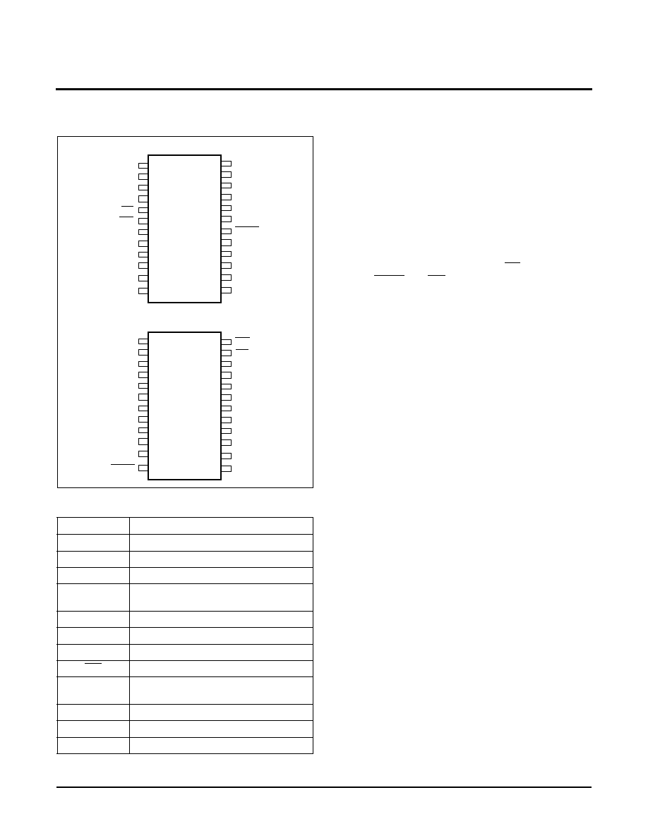
PIN CONFIGURATION
PIN NAMES
PRINCIPLES OF OPERATION
The X9440 is a highly integrated microcircuit incorpo-
rating two resistor arrays, two voltage comparators and
their associated registers and counters; and the serial
interface logic providing direct communication between
the host and the digitally-controlled potentiometers and
voltage comparators.
Serial Interface
The X9440 supports the SPI interface hardware con-
ventions. The device is accessed via the SI input with
data clocked in on the rising SCK. CS must be LOW
and the HOLD and WP pins must be HIGH during the
entire operation.
The SO and SI pins can be connected together, since
they have three state outputs. This can help to reduce
system pin count.
Array Description
The X9440 is comprised of two resistor arrays and two
voltage comparators. Each array contains 63 discrete
resistive segments that are connected in series. The
physical ends of each array are equivalent to the fixed
terminals of a mechanical potentiometer (V
H
and V
L
inputs).
At both ends of each array and between each resistor
segment is a CMOS switch connected to the wiper
(V
W
) output. Within each individual array only one
switch may be turned on at a time. These switches are
controlled by a volatile wiper counter register (WCR).
The six bits of the WCR are decoded to select, and
enable, one of sixty-four switches.
The WCR may be written directly, or it can be changed
by transferring the contents of one of four associated
data registers into the WCR. These data registers and
the WCR can be read and written by the host system.
Voltage Comparator
The comparator compares the wiper voltage V
W
with
the external input voltage V
NI
. The comparator and its
logic level output are controlled by the shutdown, latch,
and enable bits of the analog control register (ACR).
Enable connects the comparator output to the V
OUT
pin, Latch memorizes the output logic state, and shut-
down removes the analog section supply voltages to
save power. The analog control register (ACR) is pro-
grammed using the SPI serial interface.
Symbol
Description
SCK
Serial Clock
S1, SO
Serial Data
A0-A1
Device Address
V
H0
V
H1
,
V
L0
V
L1
Potentiometers (terminal equivalent)
V
W0
V
W1
Potentiometers (wiper equivalent)
V
NI0
, V
NI1
Comparator Input Voltages
V
OUT0,
V
OUT1
Buffered Comparator Outputs
WP
Hardware Write Protection
V+,V-
Analog and Voltage Comparator
Supplies
V
CC
System Supply Voltage
V
SS
System Ground
NC
No Connection
V
CC
V
L0
V
H0
WP
SI
A1
1
2
3
4
5
6
7
8
9
10
24
23
22
21
20
19
18
17
16
15
V+
V
OUT0
V
NI0
NC
A0
SO
HOLD
SCK
NC
V
NI1
SOIC
X9440
V
SS
V
W0
14
13
11
12
CS
V
L1
V
H1
V
W1
V
OUT1
V-
1
2
3
4
5
6
7
8
9
10
24
23
22
21
20
19
18
17
16
15
TSSOP
X9440
14
13
11
12
SI
A1
V
L1
V
H1
V
W1
V
SS
NC
V-
V+
V
OUT1
V
OUT0
SCK
HOLD
V
NI1
V
NI0
S0
A0
V
CC
NC
V
L0
V
H0
V
W0
WP
CS
X9440
Characteristics subject to change without notice.
4 of 22
REV 1.0 2/27/01
www.xicor.com
The ACR may be written directly, or it can be changed
by transferring the contents of one of four associated
data registers into the ACR. These data registers and
the ACR may be read and written by the host system.
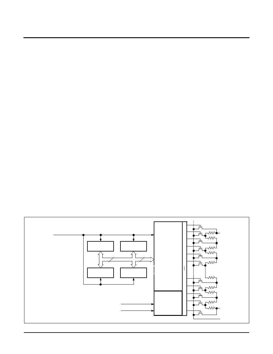
REGISTERS
Both digitally-controlled potentiometers and voltage com-
parators share the serial interface and share a common
architecture. Each potentiometer and voltage comparator
is associated with wiper counter and analog control regis-
ters and eight data registers. A detailed discussion of the
register organization and array operation follows.
Wiper Counter (WCR) and Analog Control
Registers (ACR)
The X9440 contains two wiper counter registers: one
for each XDCP potentiometer and two Analog Control
Registers, and one for each of the two voltage compar-
ators. The wiper counter register is equivalent to a
serial-in, parallel-out counter with its outputs decoded
to select one of sixty-four switches along its resistor
array. The contents of the wiper counter register and
analog control register can be altered in four ways: it
may be written directly by the host via the Write WCR
instruction (serial load); it may be written indirectly by
transferring the contents of one of four associated data
registers (DR) via the XFR data register instruction
(parallel load); it can be modified one step at a time by
the increment/ decrement instruction (WCR only).
Finally, it is loaded with the contents of its data register
zero (R0) upon power-up.
The wiper counter and analog control register are vola-
tile registers; that is, their contents are lost when the
X9440 is powered-down. Although the registers are
automatically loaded with the value in R0 upon power-
up, it should be noted this may be different from the
value present at power-down.
Programming the ACR is similar to the WCR. However,
the 6 bits in the WCR positions the wiper in the resistor
array while 3 bits in the ACR control the comparator
and its output.
Data Registers (DR)
Each potentiometer and each voltage comparator has
four non volatile data registers (DR). These can be
read or written directly by the host and data can be
transferred between any of the four data registers and
the WCR or ACR. It should be noted all operations
changing data in one of these registers is a non volatile
operation and will take a maximum of 10ms.
If the application does not require storage of multiple
settings for the potentiometer or comparator, these
registers can be used as regular memory locations that
could store system parameters or user preference
data.
Figure 1. Detailed Potentiometer Block Diagram
Serial Data Path
From Interface
Circuitry
Register 0
Register 1
Register 2
Register 3
Serial
Bus
Input
Parallel
Bus
Input
Counter
Register
Inc/Dec
Logic
UP/DN
CLK
Modified SCK
UP/DN
V
H
V
L
V
W
8
6
C
o
u
n
t
e
r
D
e
c
o
d
e
If WC = 00[H] V
W
= V
L
If WC = 3F[H] V
W
= V
H
Wiper
(One of Two Arrays)
(WCR)
X9440
Characteristics subject to change without notice.
5 of 22
REV 1.0 2/27/01
www.xicor.com
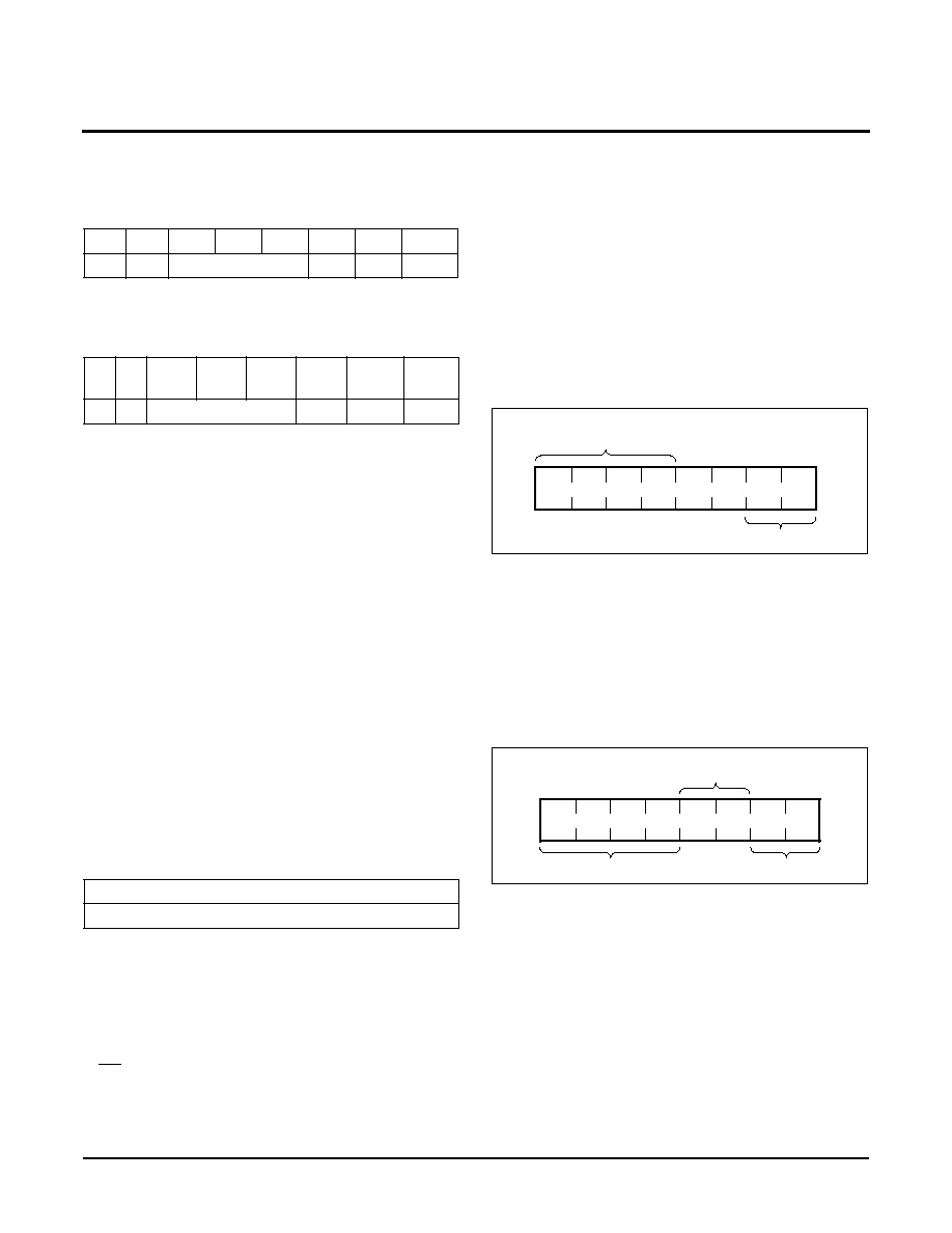
REGISTER BIT DESCRIPTIONS
Wiper Counter Register (WCR)
WP0-WP5 identify wiper position.
Analog Control Register (ACR)
Shutdown
"1"
indicates power is connected to the voltage
comparator.
"0"
indicates power is not connected to the voltage
comparator.
Enable
"1"
indicates the output buffer of the voltage
comparator is enabled.
"0"
indicates the output buffer of the voltage
comparator is disabled.
Latch
"1"
indicates the output of the voltage comparator is
memorized or latched.
"0"
indicates the output of the voltage comparator is
not latched.
Userbits--available for user applications
Data Registers (DR, R
0
R
3
)
{Refer to Memory Map, Figure 9}
INSTRUCTIONS AND PROGRAMMING
Identification (ID) Byte
The first byte sent to the X9440 from the host, following
a CS going HIGH to LOW, is called the Identification
byte. The most significant four bits of the slave address
are a device type identifier, for the X9440 this is fixed
as 0101[B] (refer to Figure 2).
The two least significant bits in the ID byte select one
of four devices on the bus. The physical device
address is defined by the state of the A
0
-A
1
input pins.
The X9440 compares the serial data stream with the
address input state; a successful compare of both
address bits is required for the X9440 to successfully
continue the command sequence. The A
0
A
1
inputs
can be actively driven by CMOS input signals or tied to
V
CC
or V
SS
.
The remaining two bits in the slave byte must be set to 0.
Figure 2. Identification Byte Format
Instruction Byte
The byte following the address contains the instruction
and register pointer information. The four most signifi-
cant bits are the instruction. The next four bits point to
one of the two pots or two voltage comparators and
when applicable they point to one of four associated
registers. The format is shown below in Figure 3.
Figure 3. Instruction Byte Format
The four high order bits of the instruction byte specify
the operation. The next two bits (R
1
and R
0
) select one
of the four data registers that is to be acted upon when
a register oriented instruction is issued. The last two
bits (P
1
and P
0
) selects which one of the four potenti-
ometers is to be affected by the instruction.
The four high order bits define the instruction. The next
two bits (R
1
and R
0
) select one of the four data registers
that is to be acted upon when a register oriented instruc-
tion is issued. The last two bits (P
1
and P
0
) select which
one of the two potentiometers or which one of the two
voltage comparators is to be affected by the instruction.
0
0
WP5 WP4 WP3 WP2 WP1
WP0
(volatile)
(LSB)
0
0
User-
bit5
User-
bit4
User-
bit3
Latc
h
En-
able
Shut-
down
(volatile)
(LSB)
Wiper Position or Analog Control Data or User Data
(Nonvolatile)
1
0
0
0
0
A1
A0
Device Type
Identifier
Device Address
1
I1
I2
I3
I0
R1
R0
P1
P0
Pot Select
Register
Select
Instructions