TL431 Programmable Precision References
FEATURES
l Programmable Output Voltage to 36 Volts
l Low Dynamic Output Impedance, 0.22
Typical
l Sink Current Capability of 1.0 to 100 mA
l Equivalent Full-Range Temperature Coefficient of
50 ppm/
o
C Typical
l Temperature Compensated for operation over
Full Rated Operating Temperature Range
l Low Output Noise Voltage
TO-92
The TL431 integrated circuits are three-terminal
programmable shunt regulator diodes. These monolithic
IC voltage references operate as a low temperature
coefficient zener which is programmable from Vref to
36 volts with two external resistors. These devices
exhibit a wide operating current range of 1.0 to 100mA
with a typical dynamic impedance of 0.22
. The
characteristics of these references make them
Pin: 1. Reference
2. Anode
3. Cathode
excellent replacements for zener diodes in many
applications such as digital voltmeters, power supplies,
and op amp circuitry. The 2.5 volt reference makes it
convenient to obtain a stable reference from 5.0 volt
logic supplies, and since the TL431 operates as a shunt
regulator, it can be used as either a positive or negative
voltage reference.
PIN ARRANGEMENT
DIP-8
Pin: 1. Cathode
6. Anode
8. Reference
Other Pins: NC
SOP-8
Pin: 1. Cathode
5. NC
2. Anode
6. Anode
3. Reference
7. Anode
4. NC
8. Reference
This SOP-8 is an internally modified SOP-8 Package.
Pins 2, 3, 6 and 7 are electrically common to the die
attach flag. This internal lead frame modification
decreases package thermal resistance and increases
power dissipation capability when appropriately
mounted on a printed circuit board. This SOP-8
conforms to all external dimensions of the standard
SOP-8 package.
CIRCUIT SCHEMATIC
ORDERING INFORMATION
FUNCTIONAL BLOCK DIAGRAM
SYMBOL
Temperature
Device
Range
Package
TL431CT
TO-92
TL431CD
0 to +70
o
C
DIP-8
TL431CS
SOP-8
TL431IT
TO-92
TL431ID
-40 to +85
o
C
DIP-8
TL431IS
SOP-8
9-1
TL431 Programmable Precision References
Rating
Symbol
Va l u e
U ni t
MAXIMUM RATINGS
(Full operating ambient temperature range applies unless otherwise noted.)
Cathode to Anode Voltage
V
KA
3 7
V
Cathode Current Range, Continuous
I
K
-100 to +150
m A
Reference Input Current Range, Continuous
I
ref
-0.05 to +10
mA
Operating Junction Temperature
T
J
1 5 0
o
C
Operating Ambient Temperature Range
T
A
o
C
TL431I, TL431AI, TL431BI
-40 to +85
TL431C, TL431AC, TL431BC
0 to +70
Storage Temperature Range
T
stg
-65 to +150
o
C
Total Power Dissipation @ T
A
= 25
o
C
P
D
W
Derate above T
A
= 25
o
C Ambient Temperature
T, S Suffix Packages
0.70
D Suffix Package
1.10
Total Power Dissipation @ T
C
= 25
o
C
P
D
W
Derate above T
A
= 25
o
C Case Temperature
T, S Suffix Packages
1.5
D Suffix Package
3.0
THERMAL CHARACTERISTICS
Characteristic
Symbol
T, S Suffix
D Suffix
Uni t
Thermal Resistance, Junction to Ambient
R
JA
1 7 8
11 4
o
C/W
Thermal Resistance, Junction to Case
R
JC
8 3
4 1
o
C/W
RECOMMENDED OPERATING CONDITIONS
Condition / Value
Symbol
M i n
Max
Unit
Thermal Resistance, Junction to Ambient
V
A
Vref
3 6
V
Thermal Resistance, Junction to Case
I
K
1.0
10 0
m A
9-2
TL431 Programmable Precision References
ELECTRICAL CHARACTERISTICS
(Ambient temperature at 25
o
C unless otherwise noted)
TL431I
TL431C
Characteristic
Symbol
M i n
Typ
Max
M i n
Typ
Max
Unit
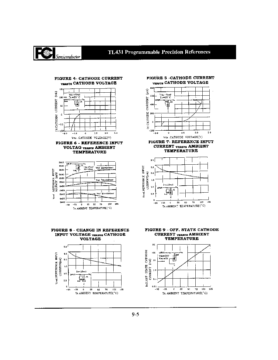
Reference Input Voltage (Fig. 1)
V
ref
V
V
KA
= V
ref
, I
K
= 10mA
T
A
= 25
o
C
2.44
2.495
2.55
2.44
2.495
2.55
T
A
= T
low
to T
high
(Note 1)
2.41
---
2.58
2.423
---
2.567
Reference Input Voltage Deviation Over
V
ref
---
7.0
30
---
3.0
17
mV
Temperature Range (Fig. 1, Note 1, 2, 4)
V
KA
= V
ref
, I
K
= 10mA
Ratio of Change in Reference Input Voltage
V
ref
mV/V
to Change in Cathode to Anode Voltage
V
KA
I
K
= 10mA (Fig. 2),
V
KA
= 10V to V
ref
---
-1.4
-2.7
---
-1.4
-2.7
V
KA
= 36V to 10V
---
-1.0
-2.0
---
-1.0
-2.0
Reference Input Current (Fig. 2)
I
ref
�
A
I
K
= 10mA, R1 = 10k, R2 =
T
A
= 25
o
C
---
1.8
4.0
---
1.8
4.0
T
A
= T
low
to T
high
(Note 1)
---
---
6.5
---
---
5.2
Reference Input Current Deviation Over
I
ref
---
0.8
2.5
---
0.4
1.2
�
A
Temperature Range (Fig. 2, Note 1, 4)
I
K
= 10mA, R1 = 10k, R2 =
Minimum Cathode Current for Regulation
I
min
---
0.5
1.0
---
0.5
1.0
mA
V
KA
= V
ref
(Fig. 1)
Off - State Cathode Current (Fig. 3)
I
off
---
260
1000
---
2.6
1000
nA
V
KA
= 36V, V
ref
= 0V
Dynamic Impedance (Fig. 1, Note 3)
Z
KA
---
0.22
0.5
---
0.22
0.5
V
KA
= V
ref
,
I
K
= 1.0mA to 100mA,
f < 1.0 kHz
8
8
ELECTRICAL CHARACTERISTICS
(Ambient temperature at 25
o
C unless otherwise noted)
TL431AI
TL431AC
TL431B
Characteristic
S ymb ol
M i n
Typ
Max
Mi n
Typ
Max
M i n
Typ
Max
U n it
Reference Input Voltage (Fig. 1)
V
ref
V
V
KA
= V
ref
, I
K
= 10mA
T
A
= 25
o
C
2.47
2.495
2.52
2.47
2.495
2.52
2.483
2.495
2.507
T
A
= T
low
to T
high
(Note 1)
2.44
---
2.55
2.453
---
2.537
2.475
2.495
2.515
Reference Input Voltage Deviation Over
V
ref
---
7.0
30
---
3.0
17
---
3.0
17
mV
Temperature Range (Fig. 1, Note 1, 2, 4)
V
KA
= V
ref
, I
K
= 10mA
Ratio of Change in Reference Input Voltage
V
ref
mV/V
to Change in Cathode to Anode Voltage
V
KA
I
K
= 10mA (Fig. 2),
V
KA
= 10V to V
ref
---
-1.4
-2.7
---
-1.4
-2.7
---
-1.4
-2.7
V
KA
= 36V to 10V
---
-1.0
-2.0
---
-1.0
-2.0
---
-1.0
-2.0
Reference Input Current (Fig. 2)
I
ref
�
A
I
K
= 10mA, R1 = 10k, R2 =
T
A
= 25
o
C
---
1.8
4.0
---
1.8
4.0
---
1.1
2.0
T
A
= T
low
to T
high
(Note 1)
---
---
6.5
---
---
5.2
---
---
4.0
Reference Input Current Deviation Over
I
ref
---
0.8
2.5
---
0.4
1.2
---
0.4
1.2
�
A
Temperature Range (Fig. 2, Note 1, 4)
I
K
= 10mA, R1 = 10k, R2 =
Minimum Cathode Current for Regulation
I
min
---
0.5
1.0
---
0.5
1.0
---
0.5
1.0
mA
V
KA
= V
ref
(Fig. 1)
Off - State Cathode Current (Fig. 3)
I
off
---
260
1000
---
260
1000
---
230
500
nA
V
KA
= 36V, V
ref
= 0V
Dynamic Impedance (Fig. 1, Note 3)
Z
KA
---
0.22
0.5
---
0.22
0.5
---
0.14
0.3
V
KA
= V
ref
,
I
K
= 1.0mA to 100mA,
f < 1.0 kHz
8
8
9-3