Description
Features
n 1500 WATT PEAK POWER PROTECTION
n EXCELLENT CLAMPING CAPABILITY
n FAST RESPONSE TIME
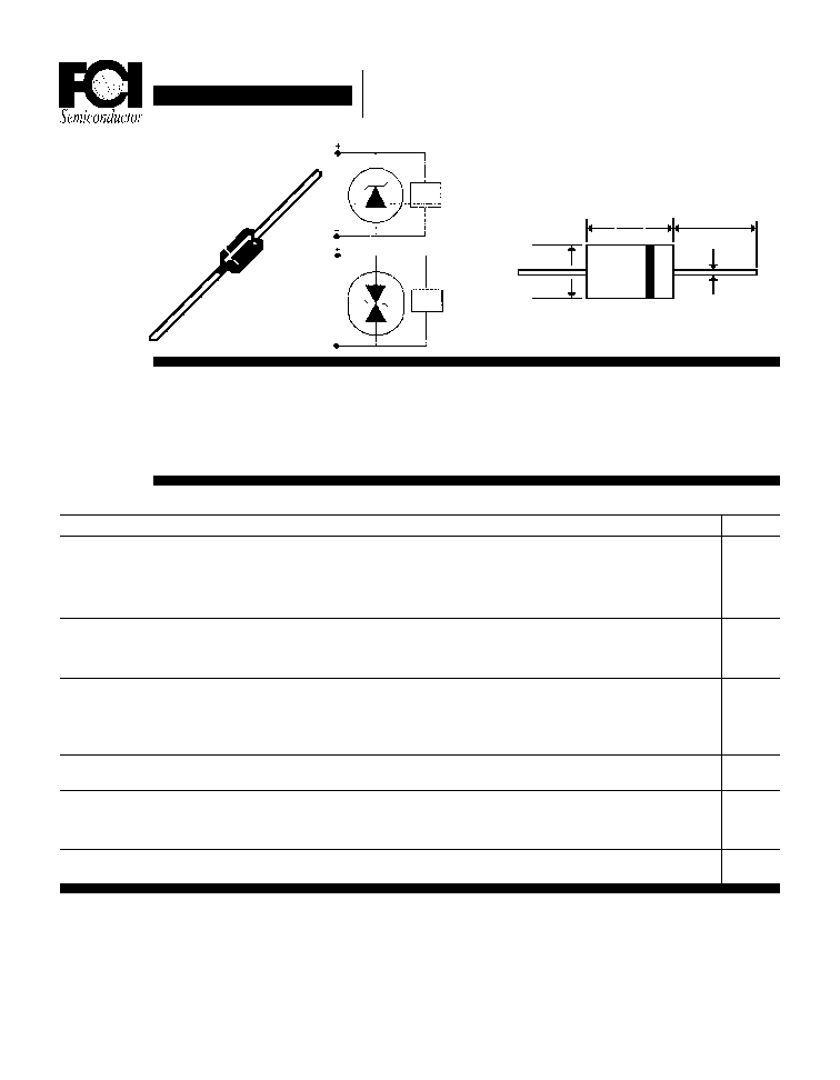
Mechanical Dimensions
n TYPICAL I
R
< 1
µ
A ABOVE 10V
n GLASS PASSIVATED CHIP CONSTRUCTION
n MEETS UL SPECIFICATION 94V-0
Maximum Ratings
Peak Power Dissipation...P
PK
T
P
= 1ms (Note 5)
Steady State Power Dissipation...P
D
@ T
L
= 75
∞
C
Non-Repetitive Peak Forward Surge Current...I
FSM
@ Rated Load Conditions, 8.3 ms, Ω Sine Wave, Single Phase
(Note 3)
Weight...G
RM
Soldering Requirements (Time & Temp)...S
T
@ 250
∞
C
Operating & Storage Temperature Range...T
J
, T
STRG
1.5KE Series
Data Sheet
6.8V to 400V GPP TRANSIENT
VOLTAGE SUPPRESSORS
1.5KE Series
Units
Watts
Watts
Amps
Grams
......................................... 1500 Min. ..........................................
............................................. 5.00 ...............................................
............................................. 200 ...............................................
............................................. 0.20 ...............................................
............................................. 11 Sec. ...........................................
......................................... -65 to 175 ..........................................
∞
C
Page 11-14
Min. to
Solder
NOTES: 1. For Bi-Directional Applications, Use C or CA. Electrical Characteristics Apply in Both Directions.
2. Mounted on 40mm
2
Copper Pads.
3. 8.3 ms, Ω Sine Wave, Single Phase Duty Cycle, @ 4 Pulses Per Minute Maximum.
4. V
BR
Measured After I
T
Applies for 300
µ
s. I
T
= Square Wave Pulse or Equivalent.
5. Non-Repetitive Current Pulse. Per Fig. 3 and Derated Above TA = 25
∞
C Per Fig. 2.
(For Bi-Polar Applications, See Note 1)
.285
.375
1.00 Min.
.050 typ.
.190
.210
JEDEC
D0-201AD
Uni-Polar
Load
TVS
Device
TVS
Device
Load
Bi-Polar

Data Sheet
6.8V to 400V GPP TRANSIENT
VOLTAGE SUPPRESSORS
Page 11-15
Ratings at
25 Deg. C ambient
temperature
unless otherwise
specified.
Single Phase Half
Wave, 60 Hz
Resistive or
Inductive Load.
For Capacitive
Load, Derate
Current by 20%.
1.5KE Series
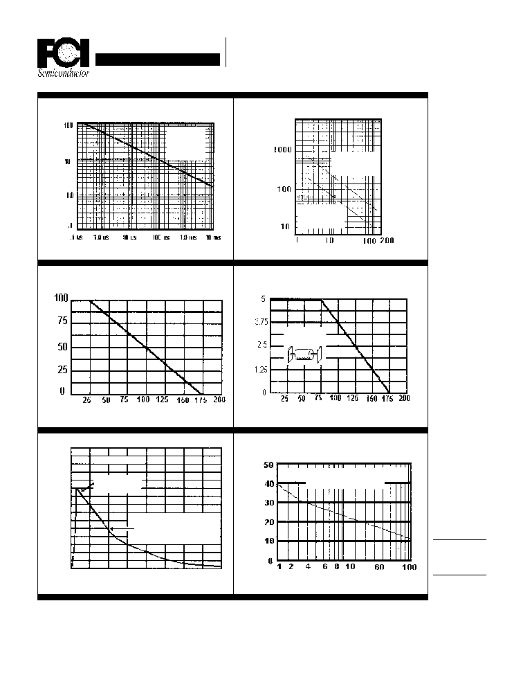
Fig. 1 Pulse Rating Curve
Fig. 4 Typical Junction Capacitance
Breakdown Voltage (V)
Fig. 2 Pulse Derating Curve
Ambient Temperature (
∞
∞
∞
∞
∞
C)
Peak Pulse Percentage
Fig. 5 Steady State Power Derating
Lead Temperature (
∞
∞
∞
∞
∞
C)
Steady State Power (W)
Fig. 3 Pulse Waveform
Peak Pulse Current
Fig. 6 Maximum Non-Repetitive
Surge Current
Number of Cycles @ 60 Hz
Peak Forward Surge Current (A)
Measured @
Standoff Voltage
Measured @
Zero Bias
0
1.0
2.0
3.0
4.0
t
r
= 10
µ
s
Peak Value
I
PPM
Pulse Width is defined
as that point where the
Peak Current decays to
50% of I
PPM
5 0
100
Time (ms)
8.3ms Single Half Sine Wave
JEDEC Method
Junction Capacitance (pF)
40 x 40 x 1mm Cu
Non-Repetitive
Pulse Waveform
Shown in Fig. 3
T
A
= 25
o
C
Pulse Width
Peak Pulse Power (kW)
