 | –≠–ª–µ–∫—Ç—Ä–æ–Ω–Ω—ã–π –∫–æ–º–ø–æ–Ω–µ–Ω—Ç: UC3842A | –°–∫–∞—á–∞—Ç—å:  PDF PDF  ZIP ZIP |

UC3842A High Performance
Current Mode Controller
l
Trimmed Oscillator Discharge Current for Precise Duty
Cycle Control
l
Current Mode Operation to 500 kHz
l
Automatic Feed Forward Compensation
l
Latching PWM for Cycle≠By≠Cycle Current Limiting
l
Internally Trimmed Reference with Undervoltage Lockout
l
High Current Totem Pole Output
l
Undervoltage Lockout with Hysteresis
l
Low Startup and Operating Current
CS SUFFIX
PLASTIC PACKAGE
SOP-14
The UC3842A series of high performance
fixed frequency current mode controllers are
specifically designed for off≠line and dc≠to≠dc
converter applications offering the designer a cost
effective solution with minimal external components.
This integrated circuit features a trimmed oscillator
for precise duty cycle control, a temperature
compensated reference, high gain error amplifier,
current sensing comparator, and a high current totem
pole output ideally suited for driving a power
MOSFET.
Also included are protective features
consisting of input and reference undervoltage lockouts
each with hysteresis, cycle≠by≠cycle current limiting,
programmable output deadtime, and a latch for single
pulse metering.
This device is available in an 8≠pin dual≠in≠
line plastic package as well as the 14≠pin plastic surface
mount (SO≠14). The SO≠14 package has separate
power and ground pins for the totem pole output
stage.
The UC3842A has UVLO thresholds of
16V(on) and 10V(off), ideally suited for off≠line
converters.
CD SUFFIX
PLASTIC PACKAGE
8 DIP
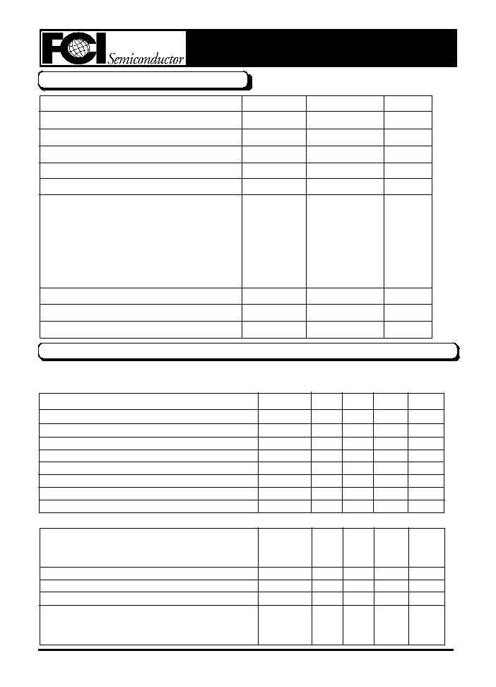
PIN CONNECTIONS
SIMPLIFIED BLOCK DIAGRAM
Pin numbers adjacent to terminals are for the D suffix 8-DIP package.
Pin numbers in parenthesis are for the S suffix SOP≠14 package.
NOTES: 1. Maximum Package power dissipation limits must be observed.
2. Adjust V
CC
above the Startup threshold before setting to 15 V.
3. Low duty cycle pulse techniques are used during test to maintain junction temperature as close to ambient as possible
T
low
= 0
∞
C, T
high
= +70
∞
C.
4. This parameter is measured at the latch trip point with V
FB
= 0V.
5. Comparator gain is defined as: A
V
V Output Compensation
V Current Sense Input
D8 SUFFIX
PLASTIC PACKAGE
8 SOP
4-12
UC3842A High Performance
Current Mode Controller
Total Power Supply and Zener Current
(I
CC
+I
Z
)
30
mA
Output Current, Source or Sink (Note 1)
I
O
1.0
A
Output Energy (Capacitive Load per Cycle)
W
5.0
µ
J
Current Sense and Voltage Feedback Inputs
V
in
-0.3 to +5.5
V
Error Amp Output Sink Current
I
O
10
mA
Power Dissipation and Thermal Characteristics
CS, D8 Suffix, SOP-14, SOP-8 Package
Maximum Power Dissipation
P
D
862
mW
Thermal Resistance, Junction to Air
R
JA
145
o
C/W
CD Suffix, 8-DIP Package
Maximum Power Dissipation
P
D
1.25
W
Thermal Resistance, Junction to Air
R
JA
100
o
C/W
Operating Ambient Temperature Range
T
A
0 to 70
o
C
Operating Junction Temperature
T
J
150
o
C
Storage Temperature Range
T
S
-65 to 150
o
C
Item
Symbol
Rating
Unit
ABSOLUTE MAXIMUM RATINGS
ELECTRICAL CHARACTERISTICS
Item
Symbol
Min
Typ
Max
Unit
Reference Output Voltage (I
O
= 1.0mA, T
J
= 25
o
C)
V
REF
4.9
5.0
5.1
V
Line Regulation (V
CC
= 12V to 25V)
Reg
line
---
2.0
20
mV
Load Regulation (I
O
= 1.0mA to 20mA)
Reg
load
---
3.0
25
mV
Temperature Stability
T
S
---
0.2
---
mV/
o
C
Total Output Variation over Line, Load, Temp.
V
REF
4.82
---
5.18
V
Output Noise Voltage (f = 10Hz to 10kHz, T
J
= 25
o
C)
V
n
---
50
---
µ
V
Long Term Stability (T
A
= 125
o
C for 1000 Hours)
S
---
5.0
---
mV
Output Short Circuit Current
ISC
-30
-85
-180
mA
V
CC
= 15V (Note 2), R
T
= 10k, CT = 3.3nF, T
A
= 0 to 70
o
C (Note 3) unless otherwise noted.
REFERENCE SECTION
Frequency
f
OSC
V
T
J
= 25
o
C
47
52
57
T
A
= 0 to 70
o
C
46
---
60
Frequency Change with Voltage (V
CC
= 12V to 25V)
f
OSC
/
V
---
0.2
1.0
%
Frequency Change with Temperature
f
OSC
/
T
---
5.0
---
%
Oscillator Voltage Swing (Peak-to-Peak)
V
OSC
---
1.6
---
V
Discharge Current (V
OSC
= 2.0V)
I
dischg
mA
T
J
= 25
o
C
7.5
8.4
9.3
T
A
= 0 to 70
o
C
7.2
---
9.5
OSCILLATOR SECTION
4-13

ELECTRICAL CHARACTERISTICS
Item
Symbol
Min
Typ
Max
Unit
Voltage Feedback Input (V
O
= 2.5V)
V
FB
2.42
2.5
2.58
V
Input Bias Current (V
FB
= 2.7V)
I
IB
---
-0.1
-2.0
µ
A
Open Loop Voltage Gain (V
O
= 2.0V to 4.0V)
A
VOL
65
90
---
dB
Unity Gain Bandwidth (T
J
= 25
o
C)
BW
0.7
1.0
---
MHz
Power Supply Rejection Ratio (V
CC
= 12V to 25V)
PSRR
60
70
---
dB
Output Current
mA
Sink (V
O
= 1.1V, V
FB
= 2.7V)
I
Sink
2.0
12
---
Source (V
O
= 5.0V, V
FB
= 2.3V)
I
Source
-0.5
-1.0
---
Output Voltage Swing
V
High State (R
L
= 15k to GND, V
FB
= 2.3V)
V
OH
5.0
6.2
---
Low State (R
L
= 15k to V
REF
, V
FB
= 2.3V)
V
OL
---
0.8
1.1
ERROR AMPLIFIER SECTION
UC3842A High Performance
Current Mode Controller
Current Sense Input Voltage Gain (Notes 4 & 5)
A
V
2.85
3.0
3.15
V/V
Maximum Current Sense Input Threshold (Note 4)
V
TH
0.9
1.0
1.1
V
Power Supply Rejection Ratio (V
CC
= 12V to 25V)
PSRR
---
70
---
dB
Input Bias Current
I
IB
---
-2.0
-10
µ
A
Propagation Delay (Current Sense Input to Output) t
PLH(in/out)
---
150
300
ns
CURRENT SENSE SECTION
Output Voltage
V
Low State
(I
Sink
= 20mA)
V
OL
---
0.1
0.4
(I
Sink
= 200mA)
---
1.6
2.2
High State
(I
Sink
= 20mA)
V
OH
13
13.5
---
(I
Sink
= 200mA)
12
13.4
---
Output Voltage with UVLO Activated
V
OL(UVLO)
V
(V
CC
= 6.0V, I
Sink
= 1.0mA)
---
0.1
1.1
Output Voltage Rise Time (C
L
= 1.0nF, T
J
= 25
o
C)
t
r
---
50
150
ns
Output Voltage Fall Time (C
L
= 1.0nF, T
J
= 25
o
C)
t
f
---
50
150
ns
OUTPUT SECTION
Startup Threshold
V
th
14.5
16
17.5
V
Minimum Operating Voltage After Turn-On
V
CC(min)
8.5
10
11.5
V
UNDERVOLTAGE LOCKOUT SECTION
Duty Cycle
Max.
DC
max
94
96
---
%
Min.
DC
min
---
---
0
PWM SECTION
Power Supply Current (V
CC
= 14V) (Note 2)
I
CC
mA
Startup
---
0.17
0.3
Operating
---
12
17
Power Supply Zener Voltage
V
Z
30
36
---
V
TOTAL DEVICE
4-14

UC3842A High Performance
Current Mode Controller
FIGURE 1 - TIMING RESISTOR versus
OSCILLATOR FREQUENCY
FIGURE 2 - OUTPUT DEADTIME versus
OSCILLATOR FREQUENCY
OSCILLATOR FREQUENCY (Hz)
TIMING RESISTOR (k
)
OSCILLATOR FREQUENCY (Hz)
PERCENT OUTPUT DEADTIME
FIGURE 4 - MAXIMUM OUTPUT DUTY CYCLE
versus TIMING RESISTOR
TIMING RESISTOR (
)
MAXIMUM OUTPUT DUTY CYCLE (%)
FIGURE 3 - OSCILLATOR DISCHARGE CURRENT
versus TEMPERATURE
AMBIENT TEMPERATURE (
o
C)
DISCHARGE CURRENT (mA)
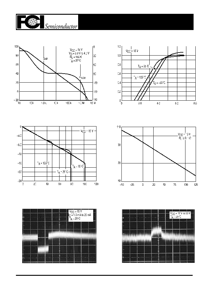
FIGURE 5 - ERROR AMP SMALL SIGNAL
TRANSIENT RESPONSE
FIGURE 6 - ERROR AMP LARGE SIGNAL
TRANSIENT RESPONSE
4-15
UC3842A High Performance
Current Mode Controller
FIGURE 7 - ERROR AMP OPEN-LOOP GAIN
AND PHASE versus FREQUENCY
FREQUENCY (Hz)
OPEN-LOOP VOL
T
AGE GAIN (dB)
EXCESS PHASE (DEGREES)
FIGURE 8 - CURRENT SENSE INPUT THRESHOLD
versus ERROR AMP OUTPUT VOLTAGE
ERROR AMP OUTPUT VOLTAGE (V)
CURRENT SENSE INPUT
THRESHOLD (V)
FIGURE 10 - REFERENCE SHORT CIRCUIT CURRENT
versus TEMPERATURE
AMBIENT TEMPERATURE (
o
C)
REFERENCE SHOR
T CIRCUIT
CURRENT (mA)
FIGURE 9 - REFERENCE VOLTAGE CHANGE
versus SOURCE CURRENT
REFERENCE SOURCE CURRENT (mA)
REFERENCE VOL
T
AGE CHANGE (mV)
FIGURE 11 - REFERENCE LOAD REGULATION
2.0 mS/DIV
OUTPUT VOL
T
AGE CHANGE (2.0mV/DIV)
FIGURE 12 - REFERENCE LINE REGULATION
2.0 mS/DIV
OUTPUT VOL
T
AGE CHANGE (2.0mV/DIV)
4-16