Preliminary Data Sheet
1.1
1
Preliminary specifications subject to change without notice
Filtronic Compound Semiconductors Ltd
Contact Details (UK): Tel: +44 (0) 1325 301111 Fax: +44 (0) 1325 306177 Email: sales@filcs.com
Contact Details (USA): Tel: +1 (408) 850 5790 Fax: +1 (408) 850 5766 Email:
sales@filcsi.com
Website: www.filcs.com
FMS2011
SP6T GaAs Multi-Band GSM Antenna Switch
Features:
Available in die form
Suitable for multi-band GSM/DCS/PCS/EDGE
applications
Excellent low control voltage performance
Excellent harmonic performance under
GSM/DCS/PCS power levels
Very high Tx-Rx isolation >45dB typ. at 1.8GHz
Very high Tx-Tx isolation >30dB typ. at 1.8GHz
Very low Tx Insertion loss
Very low control current
Description and Applications:
The FMS2011 is a low loss, high power and linear single pole six throw Gallium Arsenide antenna
switch designed for use in mobile handset applications. The die is fabricated using the Filtronic FL05
0.5
�m switch process technology which offers leading edge performance optimised for switch
applications. The FMS2011 is designed for use in dual, tri and quad � band GSM handset antenna
switch modules and RF front-end modules.
Electrical Specifications:
(T
AMBIENT
= 25�C,V
control
= 0V/2.5V, Z
IN
= Z
OUT
= 50
)
Parameter
Test Conditions
Min
Typ
Max
Units
Tx Insertion Loss
0.5 � 1.0 GHz
1.0 � 2.0 GHz
__
__
0.5
0.6
0.7
0.9
dB
dB
Rx Insertion Loss
0.5 � 1.0 GHz
1.0 � 2.0 GHz
__
__
0.6
0.8
0.8
1.2
dB
dB
Return Loss
0.5 � 2.5 GHz
__
23
__
dB
Isolation
TX-RX
0.5 � 1.0 GHz
1.0 � 2.0 GHz
30
25
33
31
__
__
dB
dB
Isolation
TX-TX
0.5 � 1.0 GHz
1.0 � 2.0 GHz
45
40
50
45
__
__
dB
dB
2nd Harmonic Level
1 GHz, Pin = +35 dBm, 100% Duty Cycle
2 GHz, Pin = +33 dBm, 100% Duty Cycle
(17:1 VSWR)
__
__
-75
-75
-70
-70
dBc
dBc
3rd Harmonic Level
1 GHz, Pin = +35 dBm, 100% Duty Cycle
2 GHz, Pin = +33 dBm, 100% Duty Cycle
(17:1 VSWR)
__
__
-75
-75
-70
-70
dBc
dBc
Switching speed : Trise, Tfall
Ton, Toff
10% to 90% RF and 90% to 10% RF
50% control to 90% RF and 50% control to 10% RF
__
__
< 0.3
< 1.0
__
__
�s
�s
Note: External DC blocking capacitors are required on all RF ports (typ: 100pF).
All unused ports terminated in 50
.
ANT
VTX1
TX1
VTX2
TX2
VRX1
RX1
VRX2
RX2
VRX3
RX3
RX4
VRX4
VRXC
ANT
VTX1
TX1
VTX2
TX2
VRX1
RX1
VRX2
RX2
VRX3
RX3
RX4
VRX4
VRXC

Preliminary Data Sheet
1.1
2
Preliminary specifications subject to change without notice
Filtronic Compound Semiconductors Ltd
Contact Details (UK): Tel: +44 (0) 1325 301111 Fax: +44 (0) 1325 306177 Email: sales@filcs.com
Contact Details (USA): Tel: +1 (408) 850 5790 Fax: +1 (408) 850 5766 Email:
sales@filcsi.com
Website: www.filcs.com
FMS2011
Absolute Maximum Ratings:
Parameter
Absolute Maximum
Max Input Power
+38dBm
Control Voltage
+8.5V
Operating Temperature
-40�C to +100�C
Storage Temperature
-55�C to +150�C
Note: Exceeding any one of these absolute maximum ratings may cause permanent damage to the
device.
Truth Table:
VRXC
VRX4
VTX2
VRX3
VRX1
VRX2
VTX1
ON
PATH
Low Low Low Low Low Low High
ANT-TX1
Low Low
High
Low Low Low Low
ANT-TX2
High Low Low Low High Low Low
ANT-RX1
High Low Low Low Low High Low
ANT-RX2
High Low Low
High Low Low Low
ANT-RX3
High High
Low Low Low Low Low
ANT-RX4
Note:
`High' =
+2.5V to +5V
`Low' =
0V to +0.2V

Preliminary Data Sheet
1.1
3
Preliminary specifications subject to change without notice
Filtronic Compound Semiconductors Ltd
Contact Details (UK): Tel: +44 (0) 1325 301111 Fax: +44 (0) 1325 306177 Email: sales@filcs.com
Contact Details (USA): Tel: +1 (408) 850 5790 Fax: +1 (408) 850 5766 Email:
sales@filcsi.com
Website: www.filcs.com
FMS2011
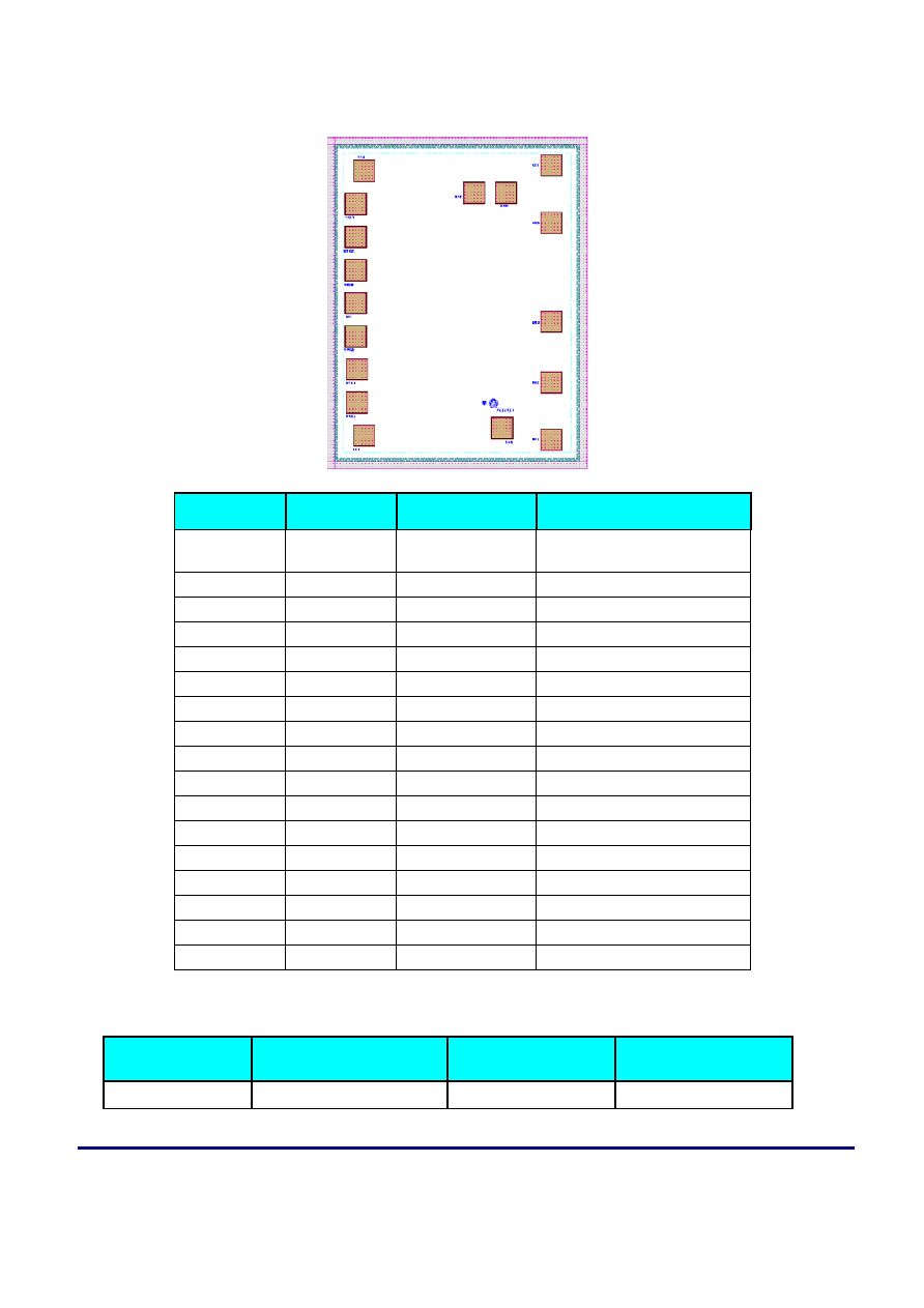
Pad and Die Layout:
Note: Co-ordinates are referenced from the bottom left hand corner of the die to the centre of the
bond pad opening
Die Size (
�m)
Die Thickness (
�m)
Min. Bond Pad
Pitch(
�m)
Min. Bond pad
opening (
�m)
900 x 1150
150 �m
111
70 x 70
Pad Number
Pad Name
Description
Pin Coordinates (�m)
A VM
Common Receive Switch
Control Voltage
99, 576
B
VRX4
RX4 Control Voltage
98, 919
C
VTX2
TX2 Control Voltage
98, 805
D
VRX3
RX3 Control Voltage
98, 689
E
VRX1
RX1 Control Voltage
103, 230
F
VRX2
RX2 Control Voltage
98, 459
G
VTX1
TX1 Control Voltage
105, 347
H
TX2
TX2 RF Output
130, 1037
I
TX1
TX1 RF Output
127, 114
J ANT Antenna
509,
958
K
RX4
RX4 RF Output
779, 1056
L
RX3
RX3 RF Output
779, 856
M
RX2
RX2 RF Output
779, 302
N
RX1
RX1 RF Output
779, 101
O GND Ground
1
605,
141
P GND Ground
1
620,
959
Q GND
Ground
RXC
777,
511
A
B
C
D
E
F
G
H
I
J
K
L
M
N
O
P
Q

Preliminary Data Sheet
1.1
4
Preliminary specifications subject to change without notice
Filtronic Compound Semiconductors Ltd
Contact Details (UK): Tel: +44 (0) 1325 301111 Fax: +44 (0) 1325 306177 Email: sales@filcs.com
Contact Details (USA): Tel: +1 (408) 850 5790 Fax: +1 (408) 850 5766 Email:
sales@filss.com
Website: www.filcs.com
FMS2011
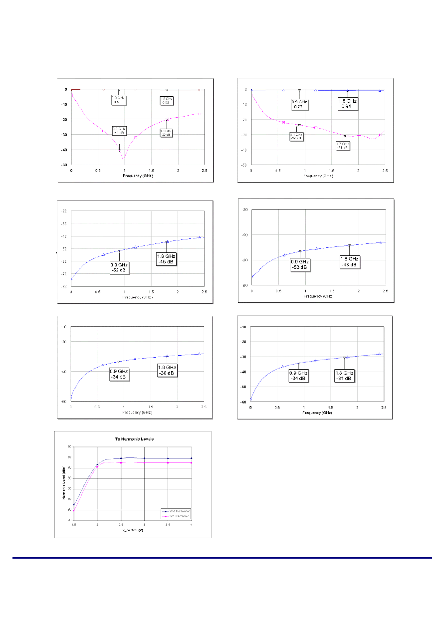
Typical Measured Performance Curves:
TX1
Loss
RX1
Loss
TX1-RX1
Isolation
TX2-RX3
Isolation
TX1-ANT
Isolation
TX2-ANT
Isolation
TX Harmonic Level


