Preliminary Data Sheet
2.1
1
Preliminary specifications subject to change without notice
Filtronic Compound Semiconductors Ltd
Contact Details (UK): Tel: +44 (0) 1325 301111 Fax: +44 (0) 1325 306177 Email: sales@filcs.com
Contact Details (USA): Tel: +1 (408) 850-5790 Fax: +1 (408) 850-5766 Email:
sales@filcsi.com
Website: www.filtronic.com
FMS2016QFN-1
High Power Reflective GaAs SP4T Switch
Features:
3x3x0.9mm Packaged pHEMT Switch
NiPdAu finish for Military and High
reliability applications
Excellent low control voltage performance
Excellent harmonic performance under
GSM/DCS/PCS/EDGE power levels
Very high isolation: >29dB at 1.8GHz
Very low Insertion loss: 0.65dB at 1.8GHz
Very low control current
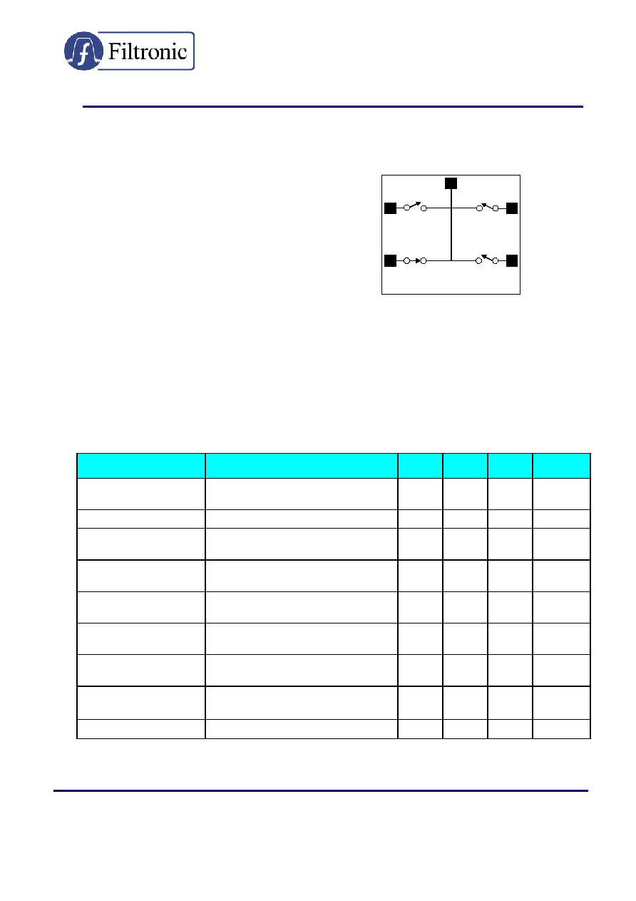
Functional Schematic
Description and Applications:
The FMS2016QFN is a low loss, high power and linear single pole four throw Gallium Arsenide
antenna switch designed for use in mobile handset applications. The die is fabricated using the
Filtronic FL05 0.5
�m switch process technology, which offers excellent performance optimised for
switch applications. The FMS2016QFN is designed for use in dual/tri and quad band GSM handset
antenna switch modules and RF front-end modules. It can also find use in other applications where
high power and linear RF switching is necessary.
Electrical Specifications:
(T
AMBIENT
= 25�C,V
ctrl
= 0V/2.5V, Z
IN
= Z
OUT
= 50
)
Parameter
Test Conditions
Min
Typ
Max
Units
Insertion Loss
0.5 � 1.0 GHz
1.0 � 2.0 GHz
<0.55
<0.65
dB
dB
Return Loss
0.5 � 2.5 GHz
20
dB
Isolation
RF1 � RF3 and RF2 � RF4
0.5 � 1.0 GHz
1.0 � 2.0 GHz
34
32
dB
dB
Isolation
RF1 � RF2
0.5 � 1.0 GHz
1.0 � 2.0 GHz
34
32
dB
dB
Isolation
RF3 � RF4
0.5 � 1.0 GHz
1.0 � 2.0 GHz
34
30
dB
dB
2nd Harmonic Level
1 GHz, Pin = +35 dBm, 100% Duty Cycle
2 GHz, Pin = +35 dBm, 100% Duty Cycle
-75
-75
dBc
dBc
3rd Harmonic Level
1 GHz, Pin = +35 dBm, 100% Duty Cycle
2 GHz, Pin = +35 dBm, 100% Duty Cycle
-75
-75
dBc
dBc
Switching speed : Trise, Tfall
Ton, Toff
10% to 90% RF and 90% to 10% RF
50% control to 90% RF and 50% control to 10% RF
<0.3
1.0
�s
�s
Control Current
+35dBm RF input @1GHz
<10
�A
Note: External DC blocking capacitors are required on all RF ports (typ: 100pF)
ANT
RF1
RF3
RF2
RF4
Preliminary Data Sheet
2.1
2
Preliminary specifications subject to change without notice
Filtronic Compound Semiconductors Ltd
Contact Details (UK): Tel: +44 (0) 1325 301111 Fax: +44 (0) 1325 306177 Email: sales@filcs.com
Contact Details (USA): Tel: +1 (408) 850-5790 Fax: +1 (408) 850-5766 Email:
sales@filcsi.com
Website: www.filtronic.com
FMS2016QFN-1
Absolute Maximum Ratings:
Parameter
Symbol
Absolute Maximum
Max Input Power
Pin
+38dBm
Control Voltage
V ctrl
+5V
Operating Temp
T oper
-40�C to +100�C
Storage Temp
T stor
-55�C to +150�C
Note: Exceeding any one of these absolute maximum ratings may cause permanent damage to the
device.
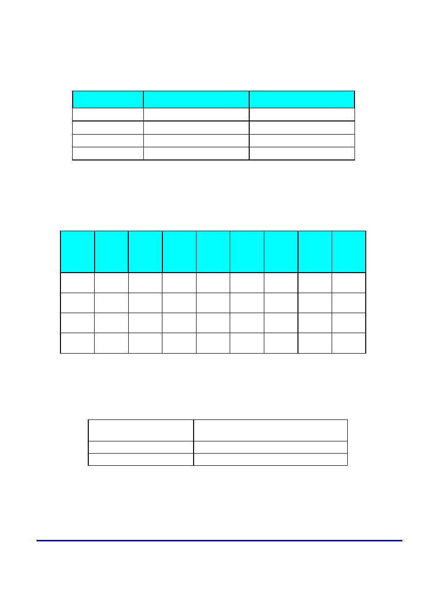
Truth Table:
Switch
State
V1
V2
V3
V4
ANT
TO
RF1
ANT
TO
RF2
ANT
TO
RF1
ANT
TO
RF2
(A)
HIGH
LOW LOW
LOW
Insertion
Loss
Isolation Isolation
Isolation
(B) LOW
HIGH
LOW LOW
Isolation
Insertion
Loss
Isolation Isolation
(C) LOW LOW
HIGH
LOW Isolation
Isolation
Insertion
Loss
Isolation
(D) LOW LOW
LOW
HIGH
Isolation Isolation
Isolation
Insertion
Loss
General Test Conditions:
Bias Voltages
LOW = 0V to 0.2V
HIGH +2.5V to +5V
Port Impedances
50
Off arm termination
50
Preliminary Data Sheet
2.1
3
Preliminary specifications subject to change without notice
Filtronic Compound Semiconductors Ltd
Contact Details (UK): Tel: +44 (0) 1325 301111 Fax: +44 (0) 1325 306177 Email: sales@filcs.com
Contact Details (USA): Tel: +1 (408) 850-5790 Fax: +1 (408) 850-5766 Email:
sales@filcsi.com
Website: www.filtronic.com
FMS2016QFN-1
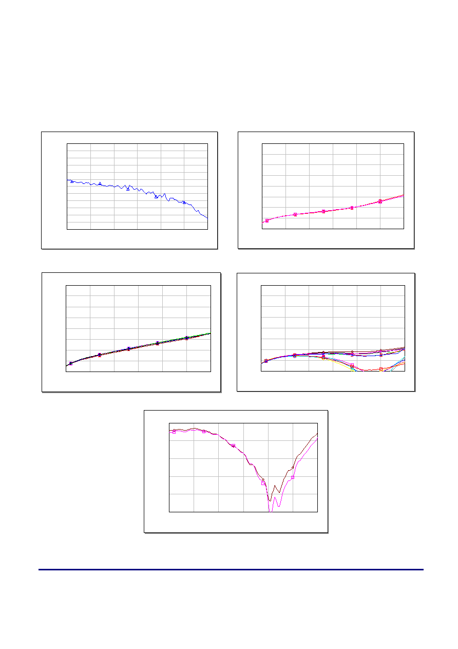
0.5
1
1.5
2
2.5
3
3.5
Frequency (GHz)
FMS2016QFN RETURN LOSS
-40
-35
-30
-25
-20
-15
dB
0.5
1
1.5
2
2.5
3
3.5
Frequency (GHz)
FMS2016QFN INSERTION LOSS
-1.2
-1.1
-1
-0.9
-0.8
-0.7
-0.6
-0.5
-0.4
-0.3
-0.2
-0.1
0
dB
0.5
1
1.5
2
2.5
3
3.5
Frequency (GHz)
FMS2016QFN RF3 to RF4 ISOLATION
-40
-35
-30
-25
-20
-15
-10
-5
0
dB
0.5
1
1.5
2
2.5
3
3.5
Frequency (GHz)
FMS2016QFN RF1 to RF3 and RF2 to RF4 ISOLATION
-40
-35
-30
-25
-20
-15
-10
-5
0
dB
0.5
1
1.5
2
2.5
3
3.5
Frequency (GHz)
FMS2016QFN RF1 to RF2 ISOLATION
-40
-35
-30
-25
-20
-15
-10
-5
0
dB
Typical Measured Performance on Evaluation Board (De-Embedded):
(Measurement Conditions V
CTRL
= 2.5V (high) & 0V (low), T
AMBIENT
= 25�C unless otherwise stated)
Preliminary Data Sheet
2.1
4
Preliminary specifications subject to change without notice
Filtronic Compound Semiconductors Ltd
Contact Details (UK): Tel: +44 (0) 1325 301111 Fax: +44 (0) 1325 306177 Email: sales@filcs.com
Contact Details (USA): Tel: +1 (408) 850-5790 Fax: +1 (408) 850-5766 Email:
sales@filcsi.com
Website: www.filtronic.com
FMS2016QFN-1
Pad Layout:
*View from the top of the package
QFN 12 Lead 3*3 Package Outline:
NiPdAu finish for Military and High reliability applications
Pin Number
Description
1 RF1
2 GND
3 RF3
4 V3
5 N/C
6 V4
7 RF4
8 GND
9 RF2
10 V2
11 ANT
RF
12 V1
PADDLE GND
8
RF2
GND
RF4
6
V1
3
4
5
12
Pin 1
RF1
V2
ANT
2
7
9
10
11
PADDLE
GND
RF3
V4
V3

Preliminary Data Sheet
2.1
5
Preliminary specifications subject to change without notice
Filtronic Compound Semiconductors Ltd
Contact Details (UK): Tel: +44 (0) 1325 301111 Fax: +44 (0) 1325 306177 Email: sales@filcs.com
Contact Details (USA): Tel: +1 (408) 988 1845 Fax: +1 (408) 970 9950 Email:
sales@filcsi.com
Website: www.filtronic.com
FMS2016QFN-1
0.5
1
1.5
2
2.5
3
3.5
Frequency (GHz)
FMS2016QFN CALIBRATION BOARD INSERTION LOSS
-1
-0.9
-0.8
-0.7
-0.6
-0.5
-0.4
-0.3
-0.2
-0.1
0
dB
0.5
1
1.5
2
2.5
3
3.5
Frequency (GHz)
FMS2016QFN CALIBRATION BOARD RETURN LOSS
-40
-35
-30
-25
-20
-15
dB
Evaluation Board:
Evaluation Board De-Embedding Data (Measured):
BOM
Label
Component
C10, C11, C12,
C13
Capacitor, 470pF, 0603
C1,C2,
C3,C4,C5
Capacitor, 100pF, 0402
C6, C7, C8, C9
Capacitor, 47pF, 0402
BOARD
Preferred evaluation board material is 0.25 mm thick
ROGERS RT4350. All RF tracks should be 50 ohm
characteristic impedance.
C11 C12
C7
C10
C3 C4
C6
C5
C8
C2
C1
C9
C13

Preliminary Data Sheet
2.1
6
Preliminary specifications subject to change without notice
Filtronic Compound Semiconductors Ltd
Contact Details (UK): Tel: +44 (0) 1325 301111 Fax: +44 (0) 1325 306177 Email: sales@filcs.com
Contact Details (USA): Tel: +1 (408) 988 1845 Fax: +1 (408) 970 9950 Email:
sales@filcsi.com
Website: www.filtronic.com
FMS2016QFN-1
Ordering Information:
Part Number
Description
FMS2016-005 Packaged
Die
FMS2016-005-EB
Packaged die mounted on evaluation board
Handling Precautions:
To avoid damage to the devices care should be exercised during handling. Proper Electrostatic
Discharge (ESD) precautions should be observed at all stages of storage, handling, assembly, and
testing. These devices should be treated as Class 1A as defined in Jedec Standard No.22-A114
(0-500V).
Further information on ESD control measures can be found in MIL-STD-1686 and MIL-HDBK-263.
Preferred Assembly Instructions:
Please refer to FCSL applications note: FAN 003 (handling and assembly of Filtronic QFN devices)
Disclaimers:
This product is not designed for use in any space based or life sustaining/supporting equipment.