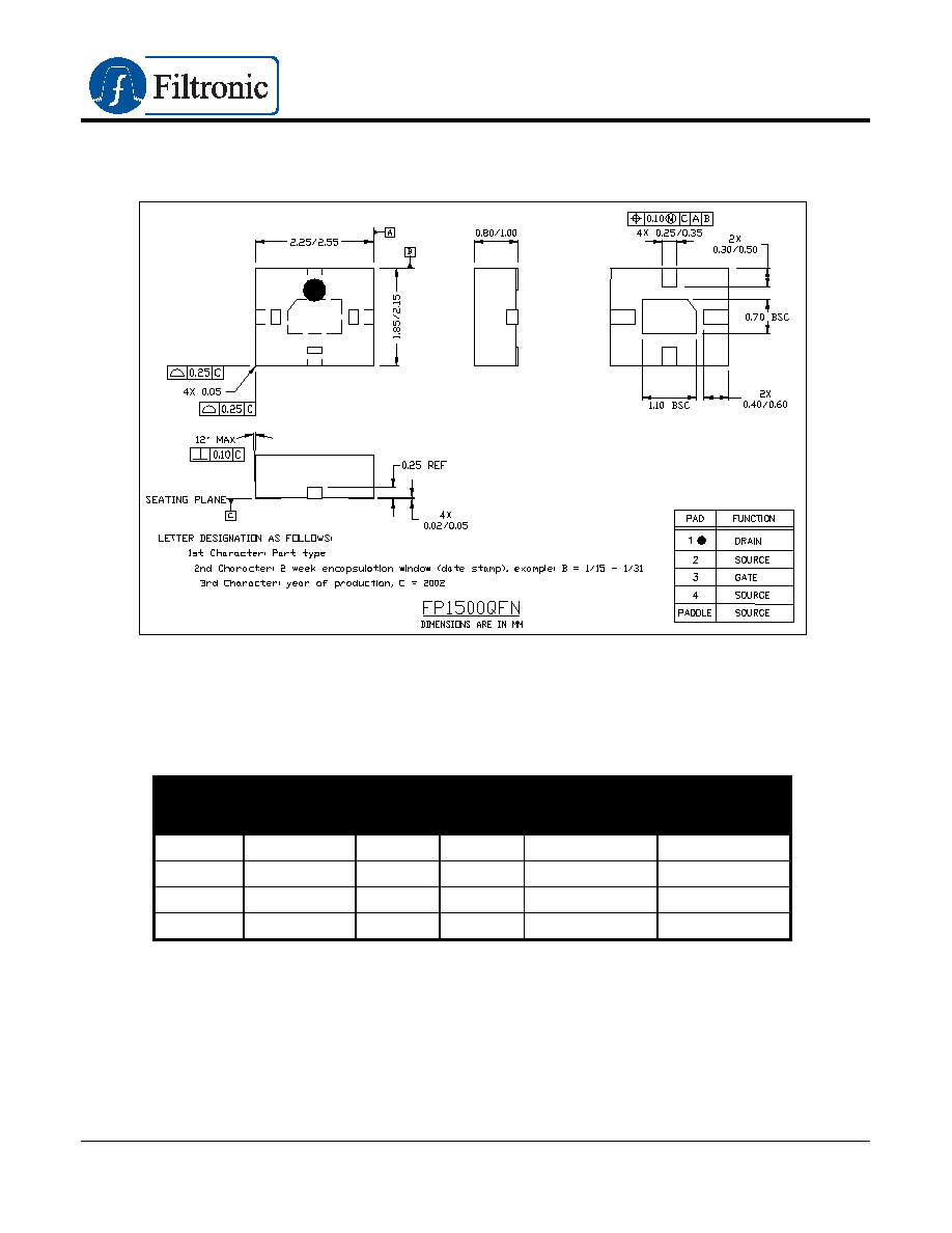
FP1500QFN
P
ACKAGED
L
OW
N
OISE
,
H
IGH
L
INEARITY
PHEMT
Phone: (408) 988-1845
http:// www.filss.com
Revised: 10/17/02
Fax: (408) 970-9950
Email: sales@filss.com
∑ FEATURES
28 dBm Output Power at 1-dB Compression
18 dB Power Gain at 2 GHz
0.8 dB Noise Figure at 2 GHz
41 dBm Output IP3
50% Power-Added Efficiency
∑ DESCRIPTION AND APPLICATIONS
The FP1500QFN is a high performance, leadless, encapsulated packaged Aluminum Gallium
Arsenide / Indium Gallium Arsenide (AlGaAs/InGaAs) pseudomorphic High Electron Mobility
Transistor (pHEMT). It utilizes a 0.25
µm x 1500 µm Schottky barrier gate, defined by electron-
beam photolithography. The recessed "mushroom" gate structure minimizes parasitic gate-source
and gate resistance. The epitaxial structure and processing have been optimized for reliable high-
power applications. The FP1500's active areas are passivated with Si
3
N
4
, and the QFN package is
ideal for low-cost, high-performance applications that require a surface-mount package. Typical
applications include drivers or output stages in PCS/Cellular amplifiers, WLL and WLAN systems,
and other types of wireless infrastructure systems up to 15 GHz.
∑ ELECTRICAL SPECIFICATIONS @ T
Ambient
= 25∞C
Parameter
Symbol
Test Conditions
Min Typ Max Units
I
DSS
V
DS
= 2 V; V
GS
= 0 V
375
420
450
mA
451
490
526
mA
Saturated Drain-Source Current
FP1500QFN-1
FP1500QFN-2
FP1500QFN-3
527
560
600
mA
Power at 1-dB Compression
P-1dB
V
DS
= 5 V; I
DS
= 50% I
DSS
27
28
dBm
Power Gain at 1-dB Compression
G-1dB
V
DS
= 5 V; I
DS
= 50% I
DSS
17
18
dB
Power-Added Efficiency
PAE
V
DS
= 5 V; I
DS
= 50% I
DSS
50
%
Noise Figure
NF
V
DS
= 5 V; I
DS
= 50% I
DSS
0.8
dB
Output Third-Order Intercept Point
IP3
V
DS
= 5V; I
DS
= 50% I
DSS
41
dBm
Maximum Drain-Source Current
I
MAX
V
DS
= 2 V; V
GS
= 1 V
563
925
mA
Transconductance
G
M
V
DS
= 2 V; V
GS
= 0 V
385
400
mS
Gate-Source Leakage Current
I
GSO
V
GS
= -5 V
10
100
µA
Pinch-Off Voltage
V
P
V
DS
= 2 V; I
DS
= 8 mA
-2.0
-1.2
-0.25
V
Gate-Source Breakdown
Voltage Magnitude
V
BDGS
I
GS
= 8 mA
-10
-12
V
Gate-Drain Breakdown
Voltage Magnitude
V
BDGD
I
GD
= 8 mA
-10
-13
V
All RF data tested at 2.0 GHz
FP1500QFN
P
ACKAGED
L
OW
N
OISE
,
H
IGH
L
INEARITY
PHEMT
Phone: (408) 988-1845
http:// www.filss.com
Revised: 10/17/02
Fax: (408) 970-9950
Email: sales@filss.com
∑ ABSOLUTE MAXIMUM RATINGS
Parameter
Symbol
Test Conditions
Min
Max
Units
Drain-Source Voltage
V
DS
T
Ambient
= 22
± 3 ∞C
6
V
Gate-Source Voltage
V
GS
T
Ambient
= 22
± 3 ∞C
-3
V
Drain-Source Current
I
DS
T
Ambient
= 22
± 3 ∞C
I
DSS
mA
Gate Current
I
G
T
Ambient
= 22
± 3 ∞C
15
mA
RF Input Power
P
IN
T
Ambient
= 22
± 3 ∞C
350
mW
Channel Operating Temperature
T
CH
T
Ambient
= 22
± 3 ∞C
175
∫C
Storage Temperature
T
STG
--
-65
175
∫C
Total Power Dissipation
P
TOT
T
Ambient
= 22
± 3 ∞C
2.7
W
Notes:
∑ Operating conditions that exceed the Absolute Maximum Ratings could result in permanent damage to the device.
∑ Power Dissipation defined as: P
TOT
(P
DC
+ P
IN
) ≠ P
OUT
, where
P
DC
: DC Bias Power
P
IN
: RF Input Power
P
OUT
: RF Output Power
∑ Absolute Maximum Power Dissipation to be de-rated as follows above 25∞C:
P
TOT
= 2.7W ≠ (0.018W/
∞C) x T
PACK
where T
PACK
= source tab lead temperature. (Bottom of the Package)
∑
This PHEMT is susceptible to damage from Electrostatic Discharge. Proper precautions should be used when handling these
devices.
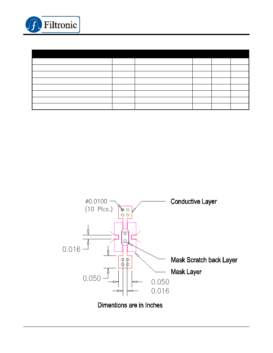
∑ PCB PAD LAYOUT
FP1500QFN
P
ACKAGED
L
OW
N
OISE
,
H
IGH
L
INEARITY
PHEMT
Phone: (408) 988-1845
http:// www.filss.com
Revised: 10/17/02
Fax: (408) 970-9950
Email: sales@filss.com
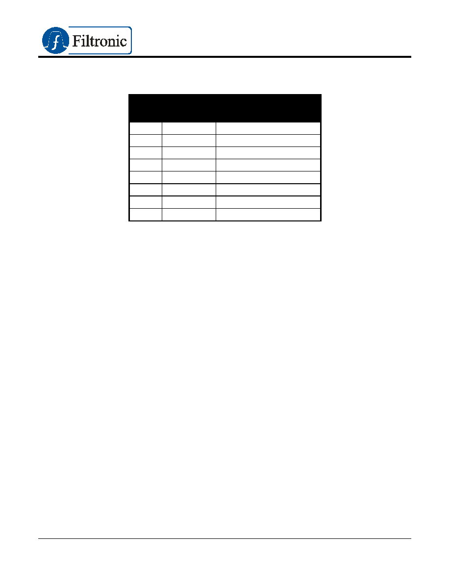
Low Noise Design
V
DS
=5V, I
DS
=125mA
Freq.
GHz
N. F. (min)
dB
Optimized Input Gamma
(
s) Mag.<Ang.
0.9
0.67
0.17<45
∞
1.8
0.76
0.33<81
∞
2.2
0.75
0.31<97.4
∞
2.4
0.80
0.32<107.9
∞
3.2
0.91
0.34<142.8
∞
4.5
1.11
0.46<163
∞
5.0
1.09
0.49<169.4
∞
6.0
1.15
0.50<-177.5
∞
∑ HANDLING PRECAUTIONS
To avoid damage to the devices care should be exercised during handling. Proper Electrostatic
Discharge (ESD) precautions should be observed at all stages of storage, handling, assembly, and
testing. These devices should be treated as Class 1A (0-500 V). Further information on ESD control
measures can be found in MIL-STD-1686 and MIL-HDBK-263.
∑ APPLICATIONS NOTES & DESIGN DATA
Applications Notes are available from your local Filtronic Sales Representative or directly from the
factory. Complete design data, including S-parameters, noise data, and large-signal models are
available on the Filtronic web site.
All information and specifications are subject to change without notice.