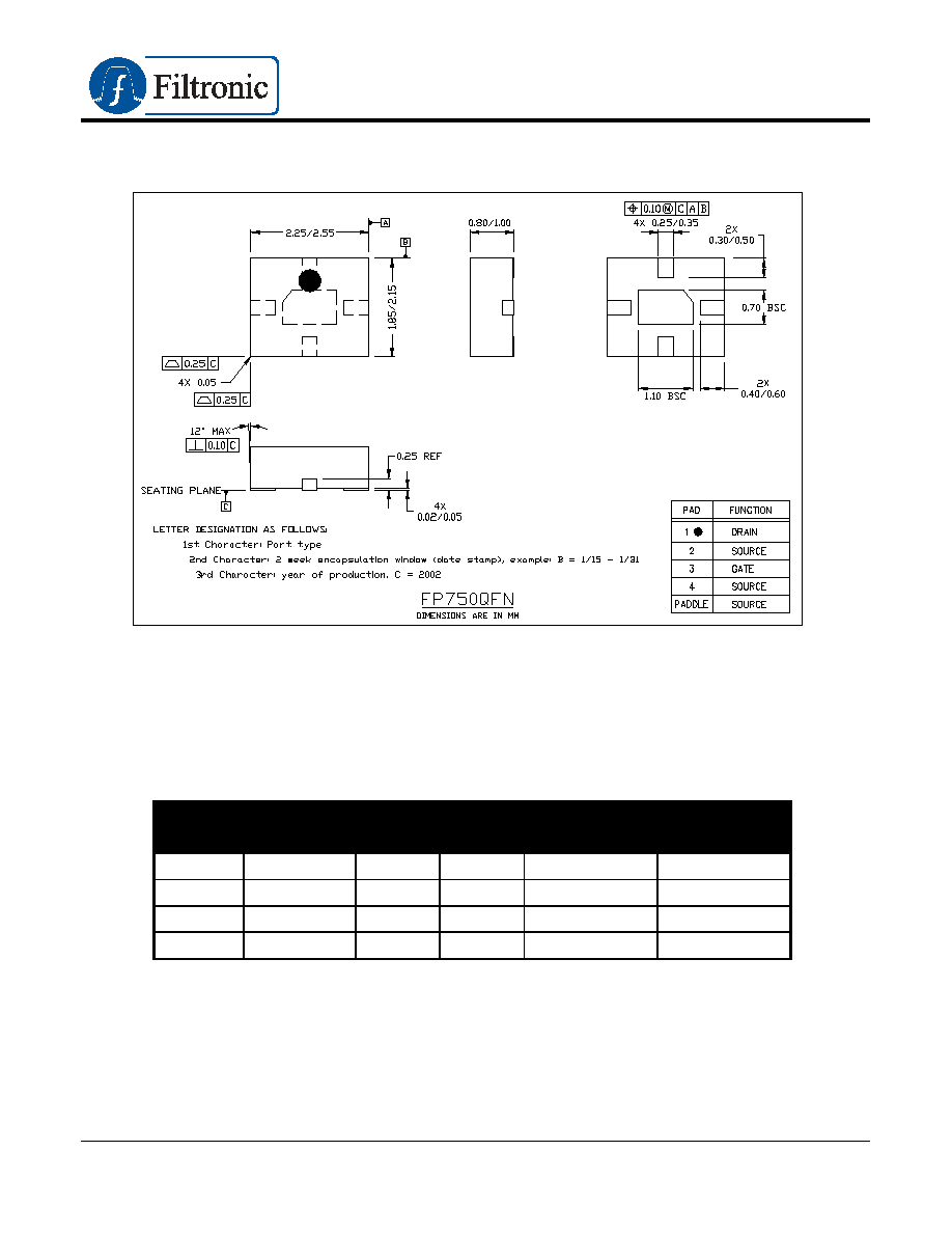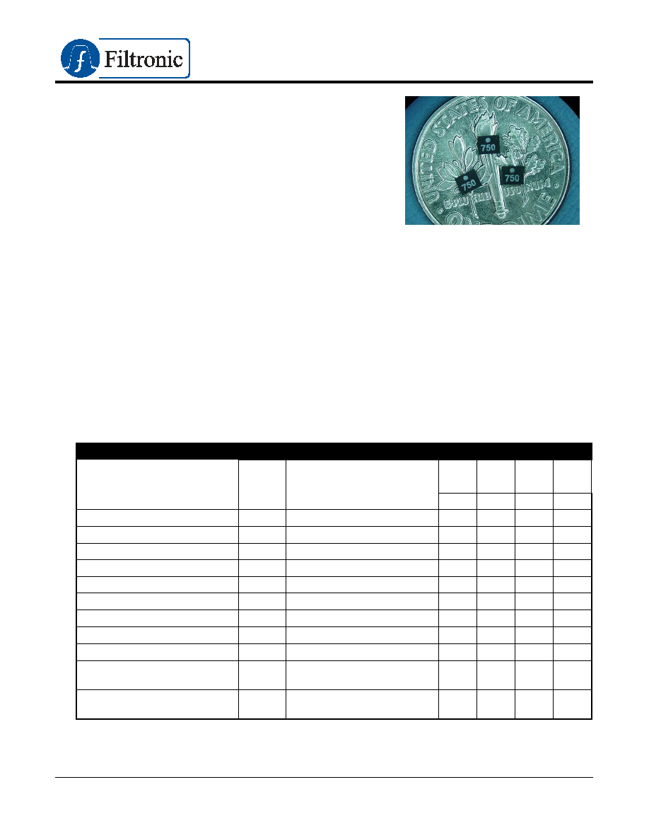
FP750QFN
P
ACKAGED
L
OW
N
OISE
,
H
IGH
L
INEARITY
PHEMT
Phone: (408) 988-1845
http:// www.filss.com
Revised: 10/17/02
Fax: (408) 970-9950
Email: sales@filss.com
∑ FEATURES
26 dBm Output Power at 1-dB Compression
19 dB Power Gain at 2 GHz
0.7 dB Noise Figure at 2 GHz
39 dBm Output IP3
55% Power-Added Efficiency
∑ DESCRIPTION AND APPLICATIONS
The FP750QFN is a high performance, leadless, encapsulated packaged AlGaAs/InGaAs/AlGaAs
pseudomorphic high electron mobility transistor (pHEMT) intended for applications requiring low
noise figure, medium output power and/or high dynamic range. It utilizes a 0.25
µm x 750 µm
Schottky barrier gate, defined by electron-beam photolithography. The FP750's active areas are
passivated with Si
3
N
4
, and the QFN package is ideal for low-cost, high-performance applications
that require a surface-mount package.
The FP750QFN is designed for commercial systems for use in low noise amplifiers and oscillators
operating over the RF and Microwave frequency ranges. The low noise figure makes it appropriate
for use in receivers in WLL/RLL, WLAN, and GPS. This device is also suitable for PCS and GSM
base station front-ends and other applications to 15 GHz.
∑ ELECTRICAL SPECIFICATIONS @ T
Ambient
= 25∞C
Parameter
Symbol
Test Conditions
Min
Typ
Max
Units
I
DSS
V
DS
= 2 V; V
GS
= 0 V
180
205
230
mA
Saturated Drain-Source Current
FP750QFN-1
FP750QFN-2
231
245
265
mA
Power at 1-dB Compression
P-1dB
V
DS
= 5 V; I
DS
= 50% I
DSS
24
26
dBm
Power Gain at 1-dB Compression
G-1dB
V
DS
= 5 V; I
DS
= 50% I
DSS
16
19
dB
Power-Added Efficiency
PAE
V
DS
= 5 V; I
DS
= 50% I
DSS
55
%
Noise Figure
NF
V
DS
= 5 V; I
DS
= 50% I
DSS
0.7
dB
Output Third-Order Intercept Point
IP3
V
DS
= 5V; I
DS
= 50% I
DSS
39
dBm
Maximum Drain-Source Current
I
MAX
V
DS
= 2 V; V
GS
= 1 V
400
mA
Transconductance
G
M
V
DS
= 2 V; V
GS
= 0 V
180
220
mS
Gate-Source Leakage Current
I
GSO
V
GS
= -5 V
5
40
µA
Pinch-Off Voltage
V
P
V
DS
= 2 V; I
DS
= 4 mA
-2.0
-1.2
-0.25
V
Gate-Source Breakdown
Voltage Magnitude
V
BDGS
I
GS
= 4 mA
-10
-12
V
Gate-Drain Breakdown
Voltage Magnitude
V
BDGD
I
GD
= 4 mA
-10
-13
V
All RF data tested at 2.0 GHz
FP750QFN
P
ACKAGED
L
OW
N
OISE
,
H
IGH
L
INEARITY
PHEMT
Phone: (408) 988-1845
http:// www.filss.com
Revised: 10/17/02
Fax: (408) 970-9950
Email: sales@filss.com
∑ ABSOLUTE MAXIMUM RATINGS
Parameter
Symbol
Test Conditions
Min
Max
Units
Drain-Source Voltage
V
DS
T
Ambient
= 22
± 3 ∞C
7
V
Gate-Source Voltage
V
GS
T
Ambient
= 22
± 3 ∞C
-3
V
Drain-Source Current
I
DS
T
Ambient
= 22
± 3 ∞C
I
DSS
mA
Gate Current
I
G
T
Ambient
= 22
± 3 ∞C
7.5
mA
RF Input Power
P
IN
T
Ambient
= 22
± 3 ∞C
175
mW
Channel Operating Temperature
T
CH
T
Ambient
= 22
± 3 ∞C
175
∫C
Storage Temperature
T
STG
--
-65
175
∫C
Total Power Dissipation
P
TOT
T
Ambient
= 22
± 3 ∞C
1.65
W
Notes:
∑ Operating conditions that exceed the Absolute Maximum Ratings could result in permanent damage to the device.
∑ Power Dissipation defined as: P
TOT
(P
DC
+ P
IN
) ≠ P
OUT
, where
P
DC
: DC Bias Power
P
IN
: RF Input Power
P
OUT
: RF Output Power
∑ Absolute Maximum Power Dissipation to be de-rated as follows above 25∞C:
P
TOT
= 1.65W ≠ (0.012W/
∞C) x T
PACK
where T
PACK
= source tab lead temperature. (Bottom of the Package)
∑
This PHEMT is susceptible to damage from Electrostatic Discharge. Proper precautions should be used when handling these
devices.
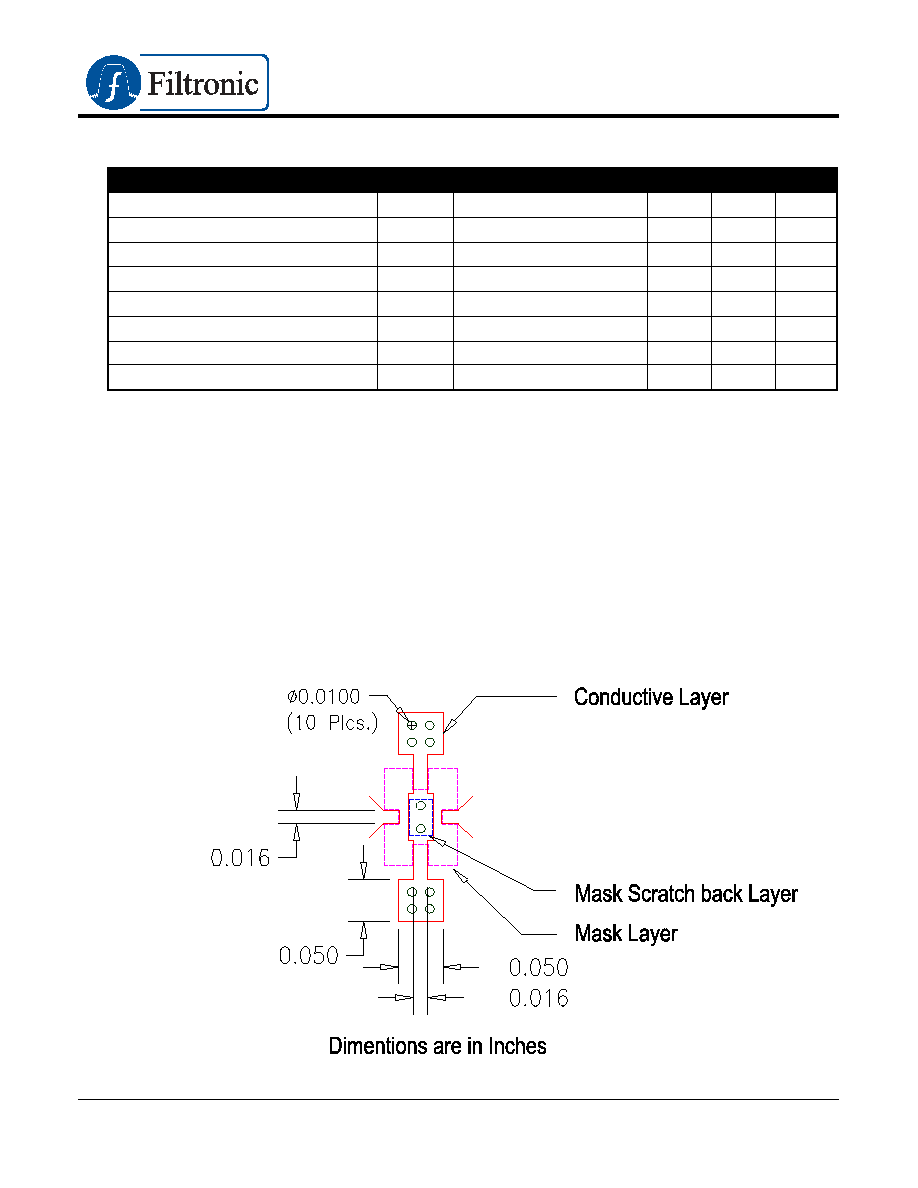
∑ PCB PAD LAYOUT
FP750QFN
P
ACKAGED
L
OW
N
OISE
,
H
IGH
L
INEARITY
PHEMT
Phone: (408) 988-1845
http:// www.filss.com
Revised: 10/17/02
Fax: (408) 970-9950
Email: sales@filss.com
Low Noise Design
V
DS
=5V, I
DS
=54mA
Freq.
GHz
N. F. (min)
dB
Optimized Input Gamma
(
s) Mag.<Ang.
0.9
0.62
0.25<20.3
∞
1.8
0.52
0.36<49.3
∞
2.2
0.57
0.33<56.2
∞
2.4
0.62
0.32<61.9
∞
3.2
0.62
0.25<90.8
∞
4.5
0.88
0.30<128.2
∞
5.0
0.90
0.32<141.6
∞
6.0
0.89
0.32<158.2
∞
∑ HANDLING PRECAUTIONS
To avoid damage to the devices care should be exercised during handling. Proper Electrostatic
Discharge (ESD) precautions should be observed at all stages of storage, handling, assembly, and
testing. These devices should be treated as Class 1A (0-500 V). Further information on ESD control
measures can be found in MIL-STD-1686 and MIL-HDBK-263.
∑ APPLICATIONS NOTES & DESIGN DATA
Applications Notes are available from your local Filtronic Sales Representative or directly from the
factory. Complete design data, including S-parameters, noise data, and large-signal models are
available on the Filtronic web site.
All information and specifications are subject to change without notice.