 | –≠–ª–µ–∫—Ç—Ä–æ–Ω–Ω—ã–π –∫–æ–º–ø–æ–Ω–µ–Ω—Ç: FPD10000V | –°–∫–∞—á–∞—Ç—å:  PDF PDF  ZIP ZIP |

PRELIMINARY
FPD10000V
10W
P
OWER P
HEMT
FOR
W
I
MAX
P
OWER
A
MPLIFIERS
Phone: +1 408 850-5790
http:/www.filtronic.co.uk/semis
Revised: 8/5/05
Fax: +1 408 850-5766
Email: sales@filcsi.com
∑
PERFORMANCE (3.5 GHz)
(802.16-2004
WiMAX
Modulation)
30 dBm Output Power, < 2.5% EVM
9.5 dB Power Gain
Class AB Efficiency 10% (10V / 1A I
DQ
)
Class B Efficiency 18% (8V / 300 mA I
DQ
)
39 dBm CW Output Power
> 48 dBm 3
rd
Order Intercept Point
Plated Source Vias ≠ No Source wirebonds needed
2.5 and 3.5 GHz Evaluation boards available (packaged device)
∑
DESCRIPTION AND APPLICATIONS
The FPD10000V is a discrete depletion mode AlGaAs/InGaAs pseudomorphic High Electron
Mobility Transistor (pHEMT), optimized for WiMAX (WMAN) IEEE 802.16 power amplifiers.
The device can be biased from Class C (I
DQ
< 200 mA), to Class A (I
DQ
= 1.0 ≠ 1.5 A) to deliver
optimal linear power over the desired output power range. The FPD10000V is also available in
packaged form.
∑
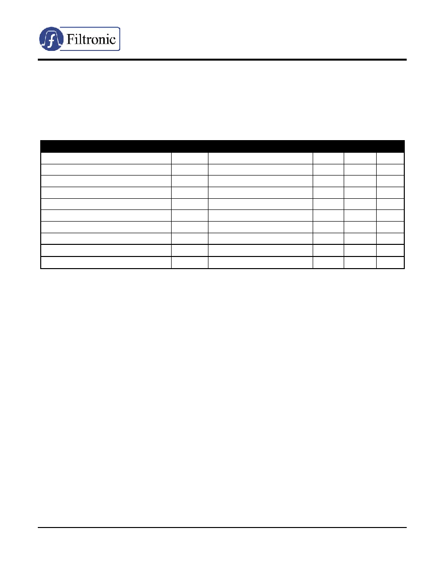
ELECTRICAL SPECIFICATIONS AT 22∞C
Parameter
Symbol
Test Conditions
Min
Typ Max Units
RF SPECIFICATIONS MEASURED AT f = 3.5 GHz
Power at 1dB Gain Compression
CW Single Tone
P
1dB
V
DS
= 10V; I
DQ
= 1.0 A
S
and
L
tuned for Optimum IP3
39.5 dBm
Power Gain at dB Gain Compression
CW Single Tone
G
1dB
V
DS
= 10V; I
DQ
= 1.0 A
Class AB Mode
9.5 dB
Channel Power with 802.16-2004
2.5% max. EVM
P
CH
Class AB Mode
V
DS
= 10 V; I
DQ
= 1.0 A
31.0 31.5 dBm
Channel Power with 802.16-2004
2.5% max. EVM
P
CH
Class B Mode
V
DS
= 8 V; I
DQ
= 350 mA typ.
29.5 30 dBm
Power-Added Efficiency
802.16-2004 modulation
Eff
Class AB Mode
Class B Mode
10
20
%
Saturated Drain-Source Current
I
DSS
V
DS
= 1.3 V; V
GS
= 0 V
5.2
A
Gate-Source Leakage Current
I
GSO
V
GS
= -3 V
3
mA
Pinch-Off Voltage
|V
P
| V
DS
= 1.3 V; I
DS
= 19 mA
1.1
V
Gate-Drain Breakdown Voltage
|V
BDGD
| I
GD
= 19 mA
30
35
V
Thermal Resistivity
CC
See Note on following page
3.5
∞C/W
GATE
BOND PAD
(16X)
DIE SIZE (
µm): 3750 x 750
DIE THICKNESS: 50
µm
BONDING PADS (
µm): >70 x 60
SEE BONDING DIAGRAM BELOW
DRAIN
BOND PAD
(16X)
PRELIMINARY
FPD10000V
10W
P
OWER P
HEMT
FOR
W
I
MAX
P
OWER
A
MPLIFIERS
Phone: +1 408 850-5790
http:/www.filtronic.co.uk/semis
Revised: 8/5/05
Fax: +1 408 850-5766
Email: sales@filcsi.com
∑
RECOMMENDED OPERATING BIAS CONDITIONS
Drain-Source Voltage:
From 6V to 12V
Quiescent Current:
From 200mA (Class B) to 1.5A (Class A)
∑
ABSOLUTE MAXIMUM RATINGS
1
Parameter
Symbol
Test Conditions
Min
Max
Units
Drain-Source Voltage
V
DS
-3V < V
GS
< +0V
15
V
Gate-Source Voltage
V
GS
0V < V
DS
< +8V
-3
V
Drain-Source Current
I
DS
For V
DS
> 2V
0.5I
DSS
mA
Gate Current
I
G
Forward or reverse current
+60/-15
mA
RF Input Power
2
P
IN
Under any acceptable bias state
2.25
W
Channel Operating Temperature
T
CH
Under any acceptable bias state
175
∫C
Storage Temperature
T
STG
Non-Operating Storage
-40
150
∫C
Total Power Dissipation
P
TOT
See De-Rating Note below
40
W
Gain Compression
Comp.
Under any bias conditions
5
dB
Simultaneous Combination of Limits
3
2 or more Max. Limits
80
%
1
T
Ambient
= 22
∞C unless otherwise noted
2
Max. RF Input Limit must be further limited if input VSWR > 2.5:1
3
Users should avoid exceeding 80% of 2 or more Limits simultaneously
Notes:
∑ Operating conditions that exceed the Absolute Maximum Ratings could result in permanent damage to the device.
∑ Thermal Resitivity specification assumes a Au/Sn eutectic die attach onto a Au-plated copper heatsink or rib.
∑ Power Dissipation defined as: P
TOT
(P
DC
+ P
IN
) ≠ P
OUT
, where
P
DC
: DC Bias Power
P
IN
: RF Input Power
P
OUT
: RF Output Power
∑ Absolute Maximum Power Dissipation to be de-rated as follows above 22∞C:
P
TOT
= 40W ≠ (0.29W/
∞C) x T
HS
where T
HS
= heatsink or ambient temperature above 22
∞C
Example: For a 85
∞C heatsink temperature: P
TOT
= 40W ≠ (0.29 x (85 ≠ 22)) = 21.7W
∑
HANDLING PRECAUTIONS
To avoid damage to the devices care should be exercised during handling. Proper Electrostatic
Discharge (ESD) precautions should be observed at all stages of storage, handling, assembly, and
testing. This product has be tested to Class 1A (> 250V but < 500V) using JESD22 A114, Human
Body Model, and to Class A, (< 200V) using JESD22 A115, Machine Model..
∑
ASSEMBLY INSTRUCTIONS
The recommended die attach is gold/tin eutectic solder under a nitrogen atmosphere. Stage
temperature should be 280-290
∞C; maximum time at temperature is one minute. The recommended
wire bond method is thermo-compression wedge bonding with 1.0 mil (0.025 mm) gold wire. Stage
temperature should be 250-260
∞C.
PRELIMINARY
FPD10000V
10W
P
OWER P
HEMT
FOR
W
I
MAX
P
OWER
A
MPLIFIERS
Phone: +1 408 850-5790
http:/www.filtronic.co.uk/semis
Revised: 8/5/05
Fax: +1 408 850-5766
Email: sales@filcsi.com
∑
APPLICATIONS NOTES & DESIGN DATA
Recommendations on matching circuits is available from your local Filtronic Sales Representative or
directly from the factory. User must ensure that proper bias sequencing is observed: Gate bias
must be applied before Drain bias, and during power-down the Drain bias must be removed
first.
∑
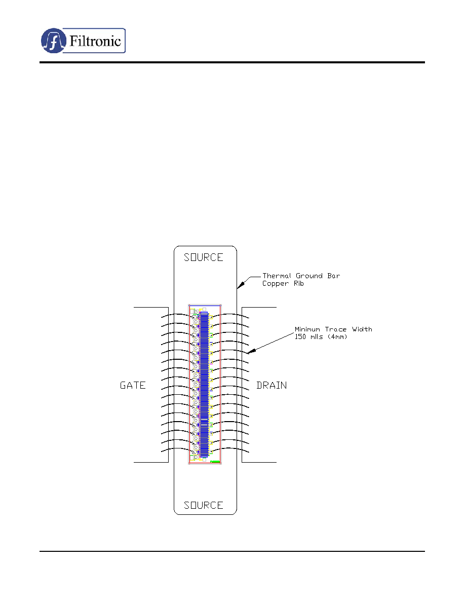
BONDING / ASSEMBLY DIAGRAM
Notes:
25
µm (0.001 in.) gold wire is recommended. No Source wire bonds are needed, device
features Source thru-vias. 16 bonds each side, Gate and Drain.
User must ensure that the die attach material is uniform and free of voiding underneath the
die to ensure proper thermal heatsinking. A useful guideline is a 0.001 ≠ 0.002 in. (0.025 ≠
0.050 mm) fillet of die attach material all around the periphery of the die.
All information and specifications are subject to change without notice.