 | –≠–ª–µ–∫—Ç—Ä–æ–Ω–Ω—ã–π –∫–æ–º–ø–æ–Ω–µ–Ω—Ç: FPD1000AS | –°–∫–∞—á–∞—Ç—å:  PDF PDF  ZIP ZIP |
FPD1000AS
1W
P
ACKAGED
P
OWER P
HEMT
Phone: +1 408 850-5790
http:// www.filtronic.co.uk/semis
Revised: 05/26/05
Fax: +1 408 850-5766
Email: sales@filcsi.com
∑
PERFORMANCE (1.8 GHz)
31 dBm Output Power (P
1dB
)
15 dB Power Gain (G
1dB
)
43 dBm Output IP3
-42 dBc WCDMA ACPR at 21 dBm P
CH
10V Operation
50% Power-Added Efficiency
Evaluation Boards Available
Design Data Available on Website
Suitable for applications to 5 GHz
∑
DESCRIPTION AND APPLICATIONS
The
FPD
1000AS is a packaged
depletion mode
AlGaAs/InGaAs pseudomorphic High Electron
Mobility Transistor (pHEMT), optimized for power applications in L-Band. The surface-mount
package has been optimized for low parasitics.
Typical applications include drivers or output stages in PCS/Cellular
base station
transmitter
amplifiers, as well as other power applications in WLL/WLAN amplifiers.
∑
ELECTRICAL SPECIFICATIONS AT 22∞C
Parameter
Symbol
Test Conditions
Min
Typ
Max
Units
RF SPECIFICATIONS MEASURED AT f = 1.8 GHz USING CW SIGNAL
Power at 1dB Gain Compression
P
1dB
V
DS
= 10V; I
DS
= 200 mA
S
and
L
tuned for Optimum IP3
30 31 dBm
Power Gain at dB Gain Compression
G
1dB
V
DS
= 10V; I
DS
= 200 mA
S
and
L
tuned for Optimum IP3
13.5 15.0
Maximum Stable Gain
S
21
/S
12
MSG V
DS
= 10 V; I
DS
= 200mA
P
IN
= 0dBm, 50
system
20 dB
Power-Added Efficiency
at 1dB Gain Compression
PAE V
DS
= 10V; I
DS
= 200 mA
S
and
L
tuned for Optimum IP3
50 %
3
rd
-Order Intermodulation Distortion
S
and
L
tuned for Optimum IP3
IM3 V
DS
= 10V; I
DS
= 200 mA
P
OUT
= 19 dBm (single-tone level)
-46
dBc
Saturated Drain-Source Current
I
DSS
V
DS
= 1.3 V; V
GS
= 0 V
480
650
800
mA
Maximum Drain-Source Current
I
MAX
V
DS
= 1.3 V; V
GS
+1 V
1100 mA
Transconductance G
M
V
DS
= 1.3 V; V
GS
= 0 V
720
mS
Gate-Source Leakage Current
I
GSO
V
GS
= -3 V
20
50
µA
Pinch-Off Voltage
|V
P
| V
DS
= 1.3 V; I
DS
= 2.4 mA
0.7
0.9
1.4
V
Gate-Source Breakdown Voltage
|V
BDGS
| I
GS
= 2.4 mA
6
8
V
Gate-Drain Breakdown Voltage
|V
BDGD
| I
GD
= 2.4 mA
20
22
V
Thermal Resistivity (channel-to-case)
CC
See Note on following page
25
∞C/W
SEE PACKAGE OUTLINE FOR
MARKING CODE

FPD1000AS
1W
P
ACKAGED
P
OWER P
HEMT
Phone: +1 408 850-5790
http:// www.filtronic.co.uk/semis
Revised: 05/26/05
Fax: +1 408 850-5766
Email: sales@filcsi.com
∑
RECOMMENDED OPERATING BIAS CONDITIONS
Drain-Source Voltage:
From 5V to 10V
Quiescent Current:
From 25% I
DSS
to 55% I
DSS
∑
ABSOLUTE MAXIMUM RATINGS
1
Parameter
Symbol
Test Conditions
Min
Max
Units
Drain-Source Voltage
V
DS
-3V < V
GS
< +0V
12
V
Gate-Source Voltage
V
GS
0V < V
DS
< +8V
-3
V
Drain-Source Current
I
DS
For V
DS
> 2V
I
DSS
mA
Gate Current
I
G
Forward / Reverse current
+20/-20
mA
RF Input Power
2
P
IN
Under any acceptable bias state
575
mW
Channel Operating Temperature
T
CH
Under any acceptable bias state
175
∫C
Storage Temperature
T
STG
Non-Operating Storage
-40
150
∫C
Total Power Dissipation
P
TOT
See De-Rating Note below
6.0
W
Gain Compression
Comp.
Under any bias conditions
5
dB
Simultaneous Combination of Limits
3
2 or more Max. Limits
80
%
1
T
Ambient
= 22
∞C unless otherwise noted
2
Max. RF Input Limit must be further limited if input VSWR > 2.5:1
3
Users should avoid exceeding 80% of 2 or more Limits simultaneously
Notes:
∑ Operating conditions that exceed the Absolute Maximum Ratings will result in permanent damage to the device.
∑ Total Power Dissipation defined as: P
TOT
(P
DC
+ P
IN
) ≠ P
OUT
, where:
P
DC
: DC Bias Power
P
IN
: RF Input Power
P
OUT
: RF Output Power
∑ Total Power Dissipation to be de-rated as follows above 22∞C:
P
TOT
= 3.5 - (0.04W/
∞C) x T
PACK
where T
PACK
= source tab lead temperature above 22
∞C
(coefficient of de-rating formula is the Thermal Conductivity)
Example: For a 55
∞C source lead temperature: P
TOT
= 6.0 - (0.04 x (55 ≠ 22)) = 4.68W
∑ For optimum heatsinking, metal-filled through (Source) via holes should be used directly below the central
metallized ground pad on the bottom of the package.
∑ Note on Thermal Resistivity: The nominal value of 25∞C/W is measured with the package mounted on a large
heatsink with thermal compound to ensure adequate (unsoldered) contact. The package temperature is referred to
the Source leads.
∑
HANDLING PRECAUTIONS
To avoid damage to the devices care should be exercised during handling. Proper Electrostatic
Discharge (ESD) precautions should be observed at all stages of storage, handling, assembly, and
testing. This product has be tested to Class 1A (> 250V but < 500V) using JESD22 A114, Human
Body Model, and to Class A, (< 200V) using JESD22 A115, Machine Model.

FPD1000AS
1W
P
ACKAGED
P
OWER P
HEMT
Phone: +1 408 850-5790
http:// www.filtronic.co.uk/semis
Revised: 05/26/05
Fax: +1 408 850-5766
Email: sales@filcsi.com
∑
BIASING GUIDELINES
Active bias circuits provide good performance stabilization over variations of operating
temperature, but require a larger number of components compared to self-bias or dual-biased.
Such circuits should include provisions to ensure that Gate bias is applied before Drain bias,
otherwise the pHEMT may be induced to self-oscillate. Contact your Sales Representative for
additional information.
Dual-bias circuits are relatively simple to implement, but will require a regulated negative
voltage supply for depletion-mode devices such as the FPD1000AS.
Self-biased circuits employ an RF-bypassed Source resistor to provide the negative Gate-Source
bias voltage, and such circuits provide some temperature stabilization for the device. A nominal
value for circuit development is 3.25
for the recommended 200mA operating point.
The recommended 200mA bias point is nominally a Class AB mode. A small amount of RF gain
expansion prior to the onset of compression is normal for this operating point.
∑
PACKAGE OUTLINE AND RECOMMENDED PC BOARD LAYOUT
(dimensions in millimeters ≠ mm)
All information and specifications subject to change without notice.
PACKAGE MARKING
CODE
Example:
f1ZD
P1F
f = Filtronic
1ZD = Lot / Date Code
P1F = Status, Part Code,
Part Type
FPD1000AS
1W
P
ACKAGED
P
OWER P
HEMT
Phone: +1 408 850-5790
http:// www.filtronic.co.uk/semis
Revised: 05/26/05
Fax: +1 408 850-5766
Email: sales@filcsi.com
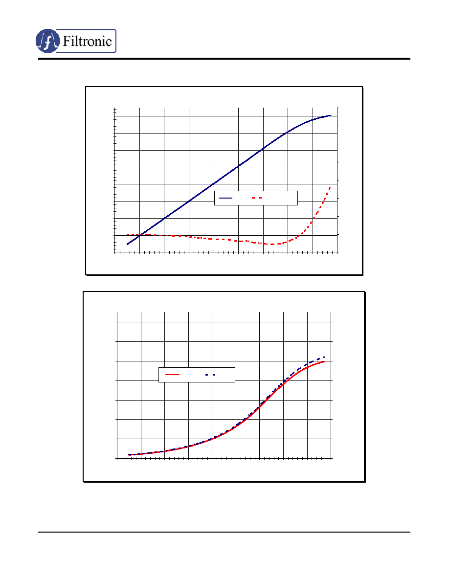
∑
TYPICAL RF PERFORMANCE (V
DS
= 10V I
DS
= 200mA
f
= 1800 MHz):
Power Transfer Characteristic
15.00
17.00
19.00
21.00
23.00
25.00
27.00
29.00
31.00
0.00
2.00
4.00
6.00
8.00
10.00
12.00
14.00
16.00
18.00
Input Power (dBm)
Output P
o
wer (dBm)
-.50
.00
.50
1.00
1.50
2.00
2.50
3.00
3.50
Gain
Com
p
ression
(
d
B)
Pout
Comp Point
Drain Efficiency and PAE
.00%
10.00%
20.00%
30.00%
40.00%
50.00%
60.00%
70.00%
0.00
2.00
4.00
6.00
8.00
10.00
12.00
14.00
16.00
18.00
Input Power (dBm)
PAE (%)
.00%
10.00%
20.00%
30.00%
40.00%
50.00%
60.00%
70.00%
Drain Efficiency (%)
PAE
Eff.
FPD1000AS
1W
P
ACKAGED
P
OWER P
HEMT
Phone: +1 408 850-5790
http:// www.filtronic.co.uk/semis
Revised: 05/26/05
Fax: +1 408 850-5766
Email: sales@filcsi.com
Note: Graph above shows Input and Output power as single carrier or single-tone levels.
IM Products vs. Input Power
17.00
19.00
21.00
23.00
25.00
27.00
2.00
3.00
4.00
5.00
6.00
7.00
8.00
9.00
10.00
11.00
12.00
Input Power (dBm)
O
u
tput Power (dB
m
)
-55.00
-50.00
-45.00
-40.00
-35.00
-30.00
-25.00
-20.00
-15.00
IM Products (dB
c
)
Pout
Im3, dBc
0
1.0
1.0
-1
.
0
10
.0
10.0
-10
.0
5.
0
5.0
-5.
0
2.0
2.
0
-2
.0
3.0
3.0
-3.
0
4.0
4.0
-4.
0
0.
2
0.2
-0.2
0.4
0.4
-0
.4
0.6
0.
6
-0
.6
0.8
0.
8
-0
.8
FPD1000AS IP3 CONTOURS 1800 MHz
Swp Max
222
Swp Min
1
46 dBm
44 dBm
42 dBm
40 dBm
48 dBm
NOTE:
IP3 contours generated with P
IN
= 11dB
back-off from P
1dB
. Local maxima for best
linearity located at:
L
= 40 + j55
and
L
= 113 + j70
with
S
= 15 + j12

FPD1000AS
1W
P
ACKAGED
P
OWER P
HEMT
Phone: +1 408 850-5790
http:// www.filtronic.co.uk/semis
Revised: 05/26/05
Fax: +1 408 850-5766
Email: sales@filcsi.com
0
1.0
1.0
-
1.0
10.
0
10.0
-10.0
5.0
5.0
-5.0
2.0
2.0
-
2.0
3.0
3.0
-3.0
4.0
4.0
-4.0
0.2
0.2
-0.2
0.4
0.4
-0.4
0.6
0.6
-
0.6
0.8
0.8
-
0.8
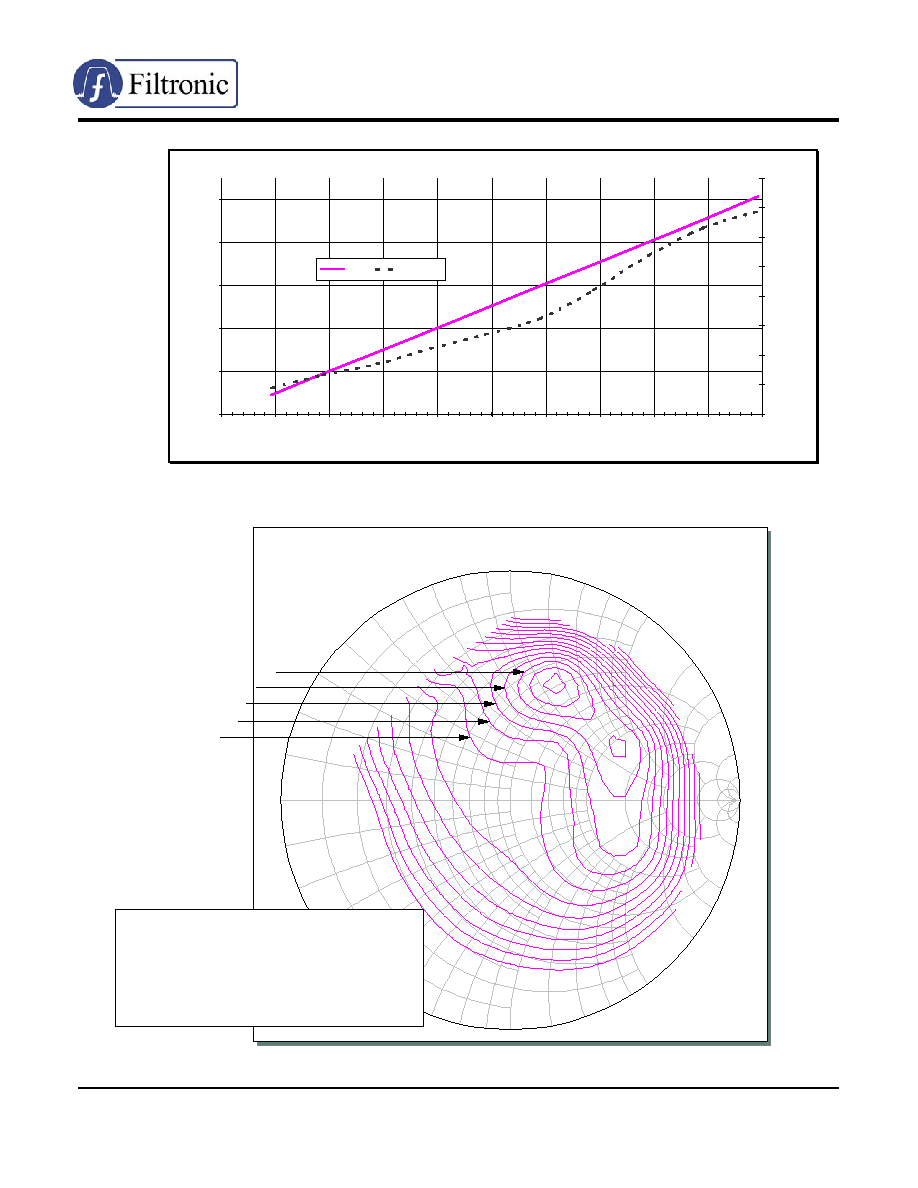
FPD1000AS POWER CONTOURS 1800 MHz
Swp Max
215
Swp Min
1
32 dBm
31 dBm
30 dBm
29 dBm
28 dBm
NOTE:
Power contours measured at constant
input power, level set to meet
nominal P1dB rating at optimum
match point. Optimum match:
S
= 3 ≠ j2
and
L
= 25 + j5
FPD1000AS I-V Curves
.000
.100
.200
.300
.400
.500
.600
.700
.800
0.00
1.00
2.00
3.00
4.00
5.00
6.00
7.00
8.00
Drain-Source Voltage (V)
Drain-Source Current (A)
VGS = 0V
VGS = -0.25V
VGS = -0.5V
VGS = -0.75V
VGS = -1.0V
VGS = -1.25V

FPD1000AS
1W
P
ACKAGED
P
OWER P
HEMT
Phone: +1 408 850-5790
http:// www.filtronic.co.uk/semis
Revised: 05/26/05
Fax: +1 408 850-5766
Email: sales@filcsi.com
∑
RF PERFORMANCE OVER FREQUENCY:
FPD1000AS at VDS = 10V and IDS = 200mA
0.0
5.0
10.0
15.0
20.0
25.0
30.0
0
500
1000
1500
2000
2500
3000
3500
4000
Frequency (MHz)
Ga
in
S21
MSG
FPD1000AS WCDMA ACPR 1900 MHz
DOWNLINK Pk/Avg = 9dB 0.01%
-60
-50
-40
-30
-20
-10
0
10
20
30
40
3
4
5
6
7
8
9
10
11
12
13
14
Input Power (dBm)
Output P
o
we
r
(
d
Bm
)
-70
-60
-50
-40
-30
-20
-10
0
AC
P
R
(
d
B
c
)
Output Power
ACPR (5 MHz)
ACPR (10MHz)

FPD1000AS
1W
P
ACKAGED
P
OWER P
HEMT
Phone: +1 408 850-5790
http:// www.filtronic.co.uk/semis
Revised: 05/26/05
Fax: +1 408 850-5766
Email: sales@filcsi.com
∑
STANDARD EVALUATION BOARD (1.70-1.85 GHZ):
See Website for complete list of Evaluation Boards
NOTE:
AutoCAD
drawing available on Website. (Model EL-BD-000011-006-A)
BILL OF MATERIALS
Designator Manufacturer's
Part
Number
Description
Quantity
C1
ATC600S3R9CW250
Capacitor, 3.9 pF, 0603, ATC 600, tol. +0.25pF 1
C2
ATC600S5R6CW250
Capacitor, 5.6 pF, 0603, ATC 600, tol. +0.25pF 1
C3
Deleted
C4
ATC600S330JW250
Capacitor, 33 pF, 0603, ATC 600, tol. +5% 1
C5
ATC600S330JW250
Capacitor, 33 pF, 0603, ATC 600, tol. +5% 1
C6
T491B105M035AS7015
Capacitor, 1 mF, SMD-B, Kemet, tol. +20% 1
C7
ATC600S680JW250
Capacitor, 68 pF, 0603, ATC 600
1
C8
T491B105M035AS7015
Capacitor, 1 mF, SMD-B, Kemet, tol. +20% 1
C9
ATC600S2R0BW250
Capacitor, 2 pF, 0603, ATC 600, tol. +0.1pF 1
L1
0604HQ-1N1
Inductor, 1.1 nH, Coilcraft High Q Surface
1
L2
0604HQ-1N1
Inductor, 1.1 nH, Coilcraft High Q Surface
1
R1
RCI-0402-27R0J
Resistor, 27 W, 0402, IMS, tol. +5% 1
R2
RCI-0603-12R0J
Resistor, 12 W, 0603, IMS, tol. +5% 1
Q1 FPD1000AS
1w
Packaged
Power pHEMT, Filtronic
1
PC-SP-000010-006
PCB, Rogers R04003, 0.012"(0.3mm), 0.5oz. Cu
1
TF-SP-000012 Carrier
1
142-0711-841
Connector, RF, SMA End Launch, Jack Assy,
2
AMP-103185-2
Connector, DC, 0.100 on center, 0.025 sq. posts,
2
TF-SP-000003
Center Block for P100 Package
1
Screw, #0-80
8
NOTE: 10-12 mil (0.3mm) plated thru vias used; vias under Q1 should be filled with Dupont CB100 conductive via
plugging material in order to achieve optimal heatsinking.
C7
C8
C6
L1
C5
R2
L2
C1
C2
R1
Q1
C4
C9
RF
INPUT
RF
OUTPUT
VDD = +10V
VGG
-0.5V