 | –≠–ª–µ–∫—Ç—Ä–æ–Ω–Ω—ã–π –∫–æ–º–ø–æ–Ω–µ–Ω—Ç: FPD2000AS | –°–∫–∞—á–∞—Ç—å:  PDF PDF  ZIP ZIP |

PRELIMINARY
FPD2000AS
2W
P
ACKAGED
P
OWER P
HEMT
Phone: +1 408 850-5790
http:// www.filcs.com
Revised: 05/03/04
Fax: +1 408 850-5766
Email: sales@filcsi.com
∑
PERFORMANCE (1.8 GHz)
33 dBm Output Power (P
1dB
)
14 dB Power Gain (G
1dB
)
46 dBm Output IP3
10V Operation
50% Power-Added Efficiency
Evaluation Boards Available
Design Data Available on Website
Usable Gain to 4GHz
∑
DESCRIPTION AND APPLICATIONS
The FPD2000AS is a packaged depletion mode AlGaAs/InGaAs pseudomorphic High Electron
Mobility Transistor (pHEMT), optimized for power applications in L-Band. The surface-mount
package has been optimized for low parasitics.
Typical applications include drivers or output stages in PCS/Cellular base station transmitter
amplifiers, as well as other power applications in WLL/WLAN amplifiers.
∑
ELECTRICAL SPECIFICATIONS AT 22∞C
Parameter
Symbol
Test Conditions
Min
Typ
Max
Units
RF SPECIFICATIONS MEASURED AT f = 1.8 GHz USING CW SIGNAL
Power at 1dB Gain Compression
P
1dB
V
DS
= 10V; I
DS
= 350 mA
S
and
L
tuned for Optimum IP3
32 33 dBm
Power Gain at dB Gain Compression
G
1dB
V
DS
= 10V; I
DS
= 350 mA
S
and
L
tuned for Optimum IP3
12.5 14.0
Maximum Stable Gain
S
21
/S
12
MSG V
DS
= 10 V; I
DS
= 350 mA
P
IN
= 0dBm, 50
system
20 dB
Power-Added Efficiency
at 1dB Gain Compression
PAE V
DS
= 10V; I
DS
= 350 mA
S
and
L
tuned for Optimum IP3
45 %
3
rd
-Order Intermodulation Distortion
IP3
V
DS
= 10V; I
DS
= 350 mA
S
and
L
tuned for Optimum IP3
P
OUT
= 22 dBm (single-tone level)
-47
-44
dBc
Saturated Drain-Source Current
I
DSS
V
DS
= 1.3 V; V
GS
= 0 V
975
1150
1325
mA
Maximum Drain-Source Current
I
MAX
V
DS
= 1.3 V; V
GS
+1 V
1800 mA
Transconductance G
M
V
DS
= 1.3 V; V
GS
= 0 V
1200
mS
Gate-Source Leakage Current
I
GSO
V
GS
= -3 V
35
85
µA
Pinch-Off Voltage
|V
P
| V
DS
= 1.3 V; I
DS
= 4 mA
0.7
0.9
1.4
V
Gate-Source Breakdown Voltage
|V
BDGS
| I
GS
= 4 mA
14
16
V
Gate-Drain Breakdown Voltage
|V
BDGD
| I
GD
= 4 mA
20
22
V
Thermal Resistivity (channel-to-case)
CC
See Note on following page
20
∞C/W
SEE PACKAGE OUTLINE FOR
MARKING CODE

PRELIMINARY
FPD2000AS
2W
P
ACKAGED
P
OWER P
HEMT
Phone: +1 408 850-5790
http:// www.filcs.com
Revised: 05/03/04
Fax: +1 408 850-5766
Email: sales@filcsi.com
∑
RECOMMENDED OPERATING BIAS CONDITIONS
Drain-Source Voltage:
From 5V to 10V
Quiescent Current:
From 25% I
DSS
to 55% I
DSS
∑
ABSOLUTE MAXIMUM RATINGS
1
Parameter
Symbol
Test Conditions
Min
Max
Units
Drain-Source Voltage
V
DS
-3V < V
GS
< +0V
12
V
Gate-Source Voltage
V
GS
0V < V
DS
< +8V
-3
V
Drain-Source Current
I
DS
For V
DS
> 2V
I
DSS
mA
Gate Current
I
G
Forward / Reverse current
+15/-2
mA
RF Input Power
2
P
IN
Under any acceptable bias state
900
mW
Channel Operating Temperature
T
CH
Under any acceptable bias state
175
∫C
Storage Temperature
T
STG
Non-Operating Storage
-40
150
∫C
Total Power Dissipation
P
TOT
See De-Rating Note below
7.6
W
Gain Compression
Comp.
Under any bias conditions
5
dB
Simultaneous Combination of Limits
3
2 or more Max. Limits
80
%
1
T
Ambient
= 22
∞C unless otherwise noted
2
Max. RF Input Limit must be further limited if input VSWR > 2.5:1
3
Users should avoid exceeding 80% of 2 or more Limits simultaneously
Notes:
∑ Operating conditions that exceed the Absolute Maximum Ratings will result in permanent damage to the device.
∑ Total Power Dissipation defined as: P
TOT
(P
DC
+ P
IN
) ≠ P
OUT
, where:
P
DC
: DC Bias Power
P
IN
: RF Input Power
P
OUT
: RF Output Power
∑ Total Power Dissipation to be de-rated as follows above 22∞C:
P
TOT
= 7.6 - (0.05W/
∞C) x T
PACK
where T
PACK
= source tab lead temperature above 22
∞C
(coefficient of de-rating formula is the Thermal Conductivity)
Example: For a 55
∞C source lead temperature: P
TOT
= 7.6 - (0.05 x (55 ≠ 22)) = 5.95W
∑ For optimum heatsinking, metal-filled through (Source) via holes should be used directly below the central
metallized ground pad on the bottom of the package.
∑ Note on Thermal Resistivity: The nominal value of 20∞C/W is measured with the package mounted on a large
heatsink with thermal compound to ensure adequate (unsoldered) contact. The package temperature is referred to
the Source leads.
∑
HANDLING PRECAUTIONS
To avoid damage to the devices care should be exercised during handling. Proper Electrostatic
Discharge (ESD) precautions should be observed at all stages of storage, handling, assembly, and
testing. These devices should be treated as Class 1A per ESD-STM5.1-1998, Human Body Model.
Further information on ESD control measures can be found in MIL-STD-1686 and MIL-HDBK-263.
PRELIMINARY
FPD2000AS
2W
P
ACKAGED
P
OWER P
HEMT
Phone: +1 408 850-5790
http:// www.filcs.com
Revised: 05/03/04
Fax: +1 408 850-5766
Email: sales@filcsi.com
∑
BIASING GUIDELINES
Active bias circuits provide good performance stabilization over variations of operating
temperature, but require a larger number of components compared to self-bias or dual-biased.
Such circuits should include provisions to ensure that Gate bias is applied before Drain bias,
otherwise the pHEMT may be induced to self-oscillate. Contact your Sales Representative for
additional information.
Dual-bias circuits are relatively simple to implement, but will require a regulated negative
voltage supply for depletion-mode devices such as the FPD2000AS.
Self-biased circuits employ an RF-bypassed Source resistor to provide the negative Gate-Source
bias voltage, and such circuits provide some temperature stabilization for the device. A nominal
value for circuit development is 1.43
for the recommended 200mA operating point. This
approach will require a DC Source resistor capable of at least 200mW dissipation.
The recommended 350mA bias point is nominally a Class AB mode. A small amount of RF gain
expansion prior to the onset of compression is normal for this operating point.
∑
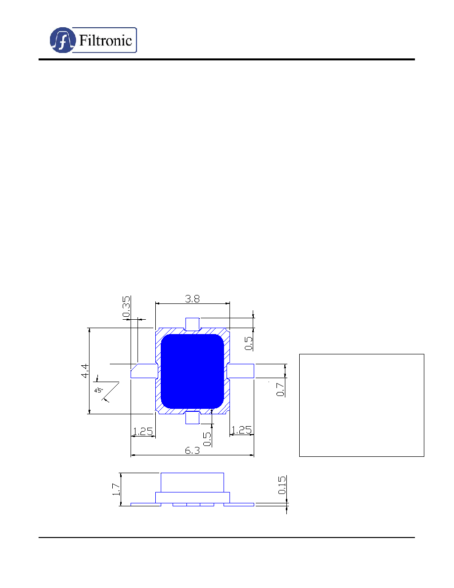
PACKAGE OUTLINE
(dimensions in millimeters ≠ mm)
All information and specifications subject to change without notice.
PACKAGE MARKING CODE
Example:
f1ZD
P2F
f = Filtronic
1ZD = Lot and Date Code
P2F = Status, Part Code, Part Type
PRELIMINARY
FPD2000AS
2W
P
ACKAGED
P
OWER P
HEMT
Phone: +1 408 850-5790
http:// www.filcs.com
Revised: 05/03/04
Fax: +1 408 850-5766
Email: sales@filcsi.com
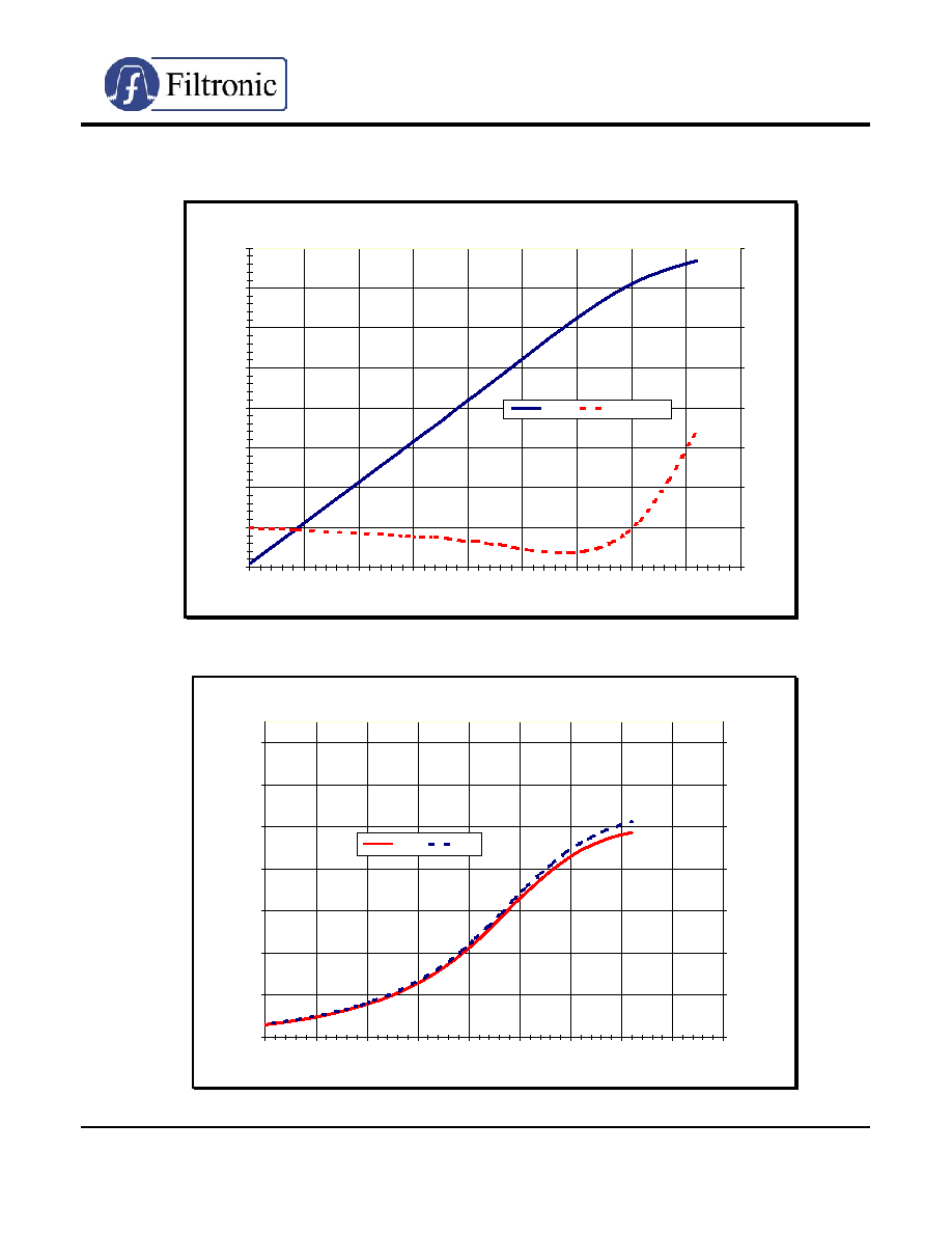
∑
TYPICAL RF PERFORMANCE (V
DS
= 10V I
DS
= 350mA
f
= 2000 MHz):
Power Transfer Characteristic
18.00
20.00
22.00
24.00
26.00
28.00
30.00
32.00
34.00
4.00
6.00
8.00
10.00
12.00
14.00
16.00
18.00
20.00
22.00
Input Power (dBm)
Output Power (dBm)
-.50
.00
.50
1.00
1.50
2.00
2.50
3.00
3.50
Gain Compression (dB)
Pout
Comp Point
Drain Efficiency and PAE
.00%
10.00%
20.00%
30.00%
40.00%
50.00%
60.00%
70.00%
6.00
8.00
10.00
12.00
14.00
16.00
18.00
20.00
22.00
24.00
Input Power (dBm)
PAE (%)
.00%
10.00%
20.00%
30.00%
40.00%
50.00%
60.00%
70.00%
D
r
ain Ef
f
i
ciency (
%
)
PAE
Eff.
PRELIMINARY
FPD2000AS
2W
P
ACKAGED
P
OWER P
HEMT
Phone: +1 408 850-5790
http:// www.filcs.com
Revised: 05/03/04
Fax: +1 408 850-5766
Email: sales@filcsi.com
Note: Graph above shows Input and Output power as single carrier or single-tone levels.
0
1.
0
1.
0
-1
.
0
10
.
0
10.0
-1
0.0
5.
0
5.0
-5.
0
2.
0
2.
0
-2
.0
3.
0
3.0
-3.
0
4.
0
4.0
-4.
0
0.
2
0.2
-0.2
0.
4
0.4
-0
.4
0.
6
0.
6
-0
.6
0.
8
0
.
8
-0
.8
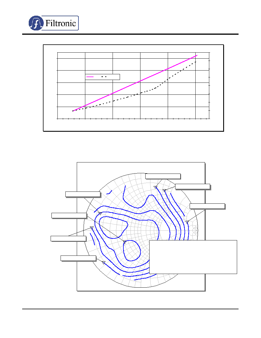
FPD2000AS IP3 CONTOURS 2 GHz
Swp Max
244
Swp Min
1
IP3_dBm = 52 dBm
IP3_dBm = 50 dBm
IP3_dBm = 48 dBm
IP3_dBm = 46 dBm
IP3_dBm = 44 dBm
IP3_dBm = 42 dBm
IP3_dBm = 40 dBm
NOTE:
IP3 contours generated with P
IN
= 11dB
back-off from P
1dB
. Local maxima for best
linearity located at:
L
= 15 + j4.5
and
L
= 28 ≠ j25
with
S
= 9.5 - j4
IM Products vs. Input Power
17.00
19.00
21.00
23.00
25.00
27.00
3.00
5.00
7.00
9.00
11.00
13.00
Input Power (dBm)
Output Power (dBm
)
-60.00
-55.00
-50.00
-45.00
-40.00
-35.00
-30.00
-25.00
-20.00
IM Pr
oduc
ts (dBc
)
Pout
Im3, dBc