FPD2250SOT89
L
OW
N
OISE
,
H
IGH
L
INEARITY
P
ACKAGED
PHEMT
Phone: +1 408 850-5790
http://www.filtronic.co.uk/semis
Revised: 01/05/05
Fax: +1 408 850-5766
Email: sales@filcsi.com
∑
PERFORMANCE (1850 MHz)
29 dBm Output Power (P
1dB
)
14 dB Small-Signal Gain (SSG)
1.0 dB Noise Figure
44 dBm Output IP3
50% Power-Added Efficiency
Evaluation Boards Available
Available in Lead Free Finish: FPD2250SOT89E
∑
DESCRIPTION AND APPLICATIONS
The FPD2250SOT89 is a packaged depletion mode AlGaAs/InGaAs pseudomorphic High Electron
Mobility Transistor (pHEMT). It utilizes a 0.25
µm x 2250 µm Schottky barrier Gate, defined by
high-resolution stepper-based photolithography. The recessed and offset Gate structure minimizes
parasitics to optimize performance, with an epitaxial structure designed for improved linearity over a
range of bias conditions and input power levels. The FPD2250 is available in die form and in other
packages.
Typical applications include drivers or output stages in PCS/Cellular base station high-intercept-
point LNAs, WLL and WLAN systems, and other types of wireless infrastructure systems.
∑
ELECTRICAL SPECIFICATIONS AT 22∞C
Parameter
Symbol
Test Conditions
Min
Typ
Max
Units
RF SPECIFICATIONS MEASURED AT f = 1850 MHz USING CW SIGNAL
Power at 1dB Gain Compression
P
1dB
V
DS
= 5 V; I
DS
= 50% I
DSS
28
29
dBm
Small-Signal Gain
SSG
V
DS
= 5 V; I
DS
= 50% I
DSS
12
14 dB
Power-Added Efficiency
PAE
V
DS
= 5 V; I
DS
= 50% I
DSS
;
P
OUT
= P
1dB
50 %
Noise Figure
NF
V
DS
= 5 V; I
DS
= 50% I
DSS
V
DS
= 5 V; I
DS
= 25% I
DSS
1.0
0.8
1.2 dB
Output Third-Order Intercept Point
(from 15 to 5 dB below P
1dB
)
IP3 V
DS
= 5V; I
DS
= 50% I
DSS
Matched for optimal power
Matched for best IP3
43
44
dBm
Saturated Drain-Source Current
I
DSS
V
DS
= 2 V; V
GS
= 0 V
560
700
825
mA
Maximum Drain-Source Current
I
MAX
V
DS
= 2 V; V
GS
+1 V
1.1 A
Transconductance G
M
V
DS
= 2 V; V
GS
= 0 V
600
mS
Gate-Source Leakage Current
I
GSO
V
GS
= -5 V
1
10
µA
Pinch-Off Voltage
|V
P
| V
DS
= 2 V; I
DS
= 2.25 mA
0.7
1.0
1.3
V
Gate-Source Breakdown Voltage
|V
BDGS
| I
GS
= 2.25 mA
12
16
V
Gate-Drain Breakdown Voltage
|V
BDGD
| I
GD
= 2.25 mA
12
18
V

FPD2250SOT89
L
OW
N
OISE
,
H
IGH
L
INEARITY
P
ACKAGED
PHEMT
Phone: +1 408 850-5790
http://www.filtronic.co.uk/semis
Revised: 01/05/05
Fax: +1 408 850-5766
Email: sales@filcsi.com
∑
ABSOLUTE MAXIMUM RATINGS
1
Parameter
Symbol
Test Conditions
Min
Max
Units
Drain-Source Voltage
V
DS
-3V < V
GS
< +0V
8
V
Gate-Source Voltage
V
GS
0V < V
DS
< +8V
-3
V
Drain-Source Current
I
DS
For V
DS
> 2V
I
DSS
mA
Gate Current
I
G
Forward or reverse current
22
mA
RF Input Power
2
P
IN
Under any acceptable bias state
525
mW
Channel Operating Temperature
T
CH
Under any acceptable bias state
175
∫C
Storage Temperature
T
STG
Non-Operating Storage
-40
150
∫C
Total Power Dissipation
P
TOT
See De-Rating Note below
2.5
W
Gain Compression
Comp.
Under any bias conditions
5
dB
Simultaneous Combination of Limits
3
2 or more Max. Limits
80
%
1
T
Ambient
= 22
∞C unless otherwise noted
2
Max. RF Input Limit must be further limited if input VSWR > 2.5:1
3
Users should avoid exceeding 80% of 2 or more Limits simultaneously
Notes:
∑ Operating conditions that exceed the Absolute Maximum Ratings will result in permanent damage to the device.
∑ Total Power Dissipation defined as: P
TOT
(P
DC
+ P
IN
) ≠ P
OUT
, where:
P
DC
: DC Bias Power
P
IN
: RF Input Power
P
OUT
: RF Output Power
∑ Total Power Dissipation to be de-rated as follows above 22∞C:
P
TOT
= 2.5W ≠ (0.017W/
∞C) x T
PACK
where T
PACK
= source tab lead temperature above 22
∞C
(coefficient of de-rating formula is the Thermal Conductivity)
Example: For a 65
∞C source lead temperature: P
TOT
= 2.5W ≠ (0.017 x (65 ≠ 22)) = 1.78W
∑
HANDLING PRECAUTIONS
To avoid damage to the devices care should be exercised during handling. Proper Electrostatic
Discharge (ESD) precautions should be observed at all stages of storage, handling, assembly, and
testing. These devices should be treated as Class 1A per ESD-STM5.1-1998, Human Body Model.
Further information on ESD control measures can be found in MIL-STD-1686 and MIL-HDBK-263.
∑
APPLICATIONS NOTES & DESIGN DATA
Applications Notes are available from your local Filtronic Sales Representative or directly from the
factory. Complete design data, including S-parameters, noise data, and large-signal models are
available on the Filtronic web site. Evaluation Boards available upon request.
FPD2250SOT89
L
OW
N
OISE
,
H
IGH
L
INEARITY
P
ACKAGED
PHEMT
Phone: +1 408 850-5790
http://www.filtronic.co.uk/semis
Revised: 01/05/05
Fax: +1 408 850-5766
Email: sales@filcsi.com
∑
BIASING GUIDELINES
Active bias circuits provide good performance stabilization over variations of operating
temperature, but require a larger number of components compared to self-bias or dual-biased.
Such circuits should include provisions to ensure that Gate bias is applied before Drain bias,
otherwise the pHEMT may be induced to self-oscillate. Contact your Sales Representative for
additional information.
Dual-bias circuits are relatively simple to implement, but will require a regulated negative
voltage supply for depletion-mode devices such as the FPD2250SOT89.
Self-biased circuits employ an RF-bypassed Source resistor to provide the negative Gate-Source
bias voltage, and such circuits provide some temperature stabilization for the device. A nominal
value for circuit development is 2.0
for a 50% of I
DSS
operating point.
For standard Class A operation, a 50% of I
DSS
bias point is recommended. A small amount of
RF gain expansion prior to the onset of compression is normal for this operating point. Note that
pHEMTs, since they are "quasi- E/D mode" devices, exhibit Class AB traits when operated at
50% of I
DSS
. To achieve a larger separation between P
1dB
and IP3, an operating point in the 25%
to 33% of I
DSS
range is suggested. Such Class AB operation will not degrade the IP3
performance.
∑
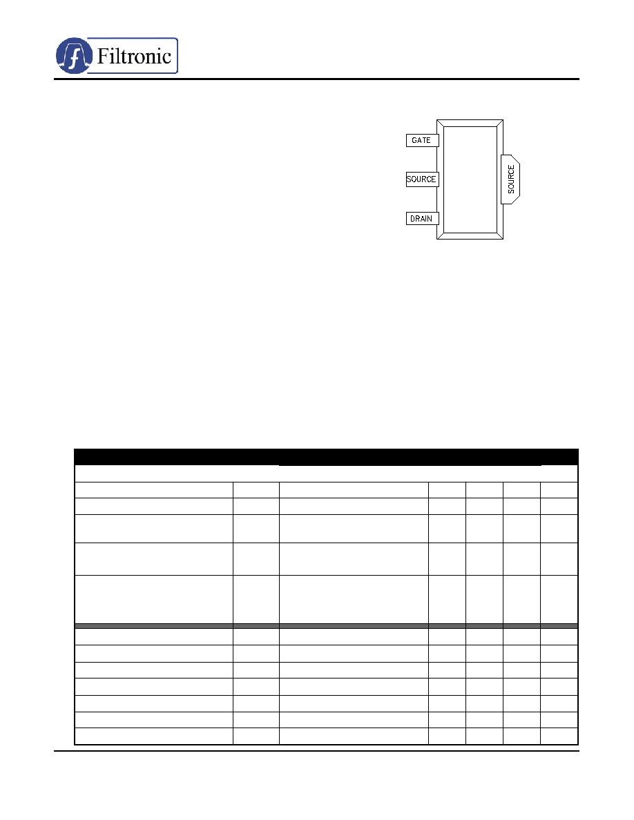
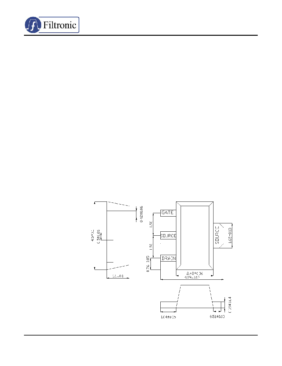
PACKAGE OUTLINE
(dimensions in mm)
All information and specifications subject to change without notice.
FPD2250SOT89
L
OW
N
OISE
,
H
IGH
L
INEARITY
P
ACKAGED
PHEMT
Phone: +1 408 850-5790
http://www.filtronic.co.uk/semis
Revised: 01/05/05
Fax: +1 408 850-5766
Email: sales@filcsi.com
∑
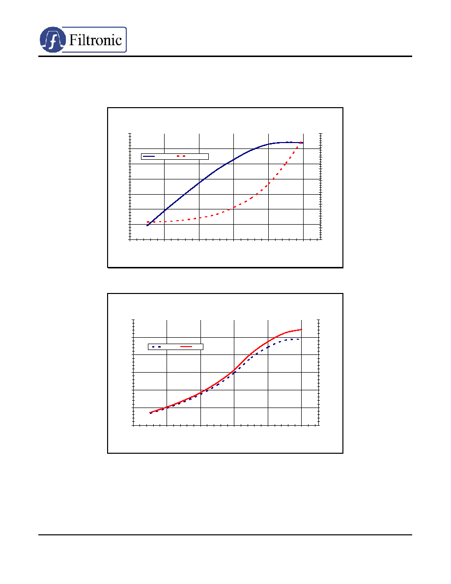
TYPICAL TUNED RF PERFORMANCE
Typical power and efficiency is shown above. The devices were biased nominally at V
DS
= 5V, I
DS
= 50% of I
DSS
, at a test frequency of 1.85 GHz. The test devices were tuned (input and output
tuning) for maximum output power at 1dB gain compression.
Power Transfer Characteristric
VDS = 5V IDS = 50% IDSS at f = 1.85 GHz
23.0
24.0
25.0
26.0
27.0
28.0
29.0
30.0
9
11
13
15
17
19
Input Power (dBm)
Out
put
P
o
wer (d
Bm
)
-0.75
-0.25
0.25
0.75
1.25
1.75
2.25
2.75
3.25
3.75
Gai
n C
o
m
pressio
n
(
d
B
)
Pout (dBm)
Comp Point
Drain Efficiency and PAE
VDS = 5V IDS = 50% IDSS at f = 1.85 GHz
5.0%
15.0%
25.0%
35.0%
45.0%
55.0%
65.0%
9
11
13
15
17
19
Input Power (dBm)
PA
E
(
%
)
5.0%
15.0%
25.0%
35.0%
45.0%
55.0%
65.0%
D
a
in
E
f
f
i
ciency
(%
)
PAE
Eff.
FPD2250SOT89
L
OW
N
OISE
,
H
IGH
L
INEARITY
P
ACKAGED
PHEMT
Phone: +1 408 850-5790
http://www.filtronic.co.uk/semis
Revised: 01/05/05
Fax: +1 408 850-5766
Email: sales@filcsi.com
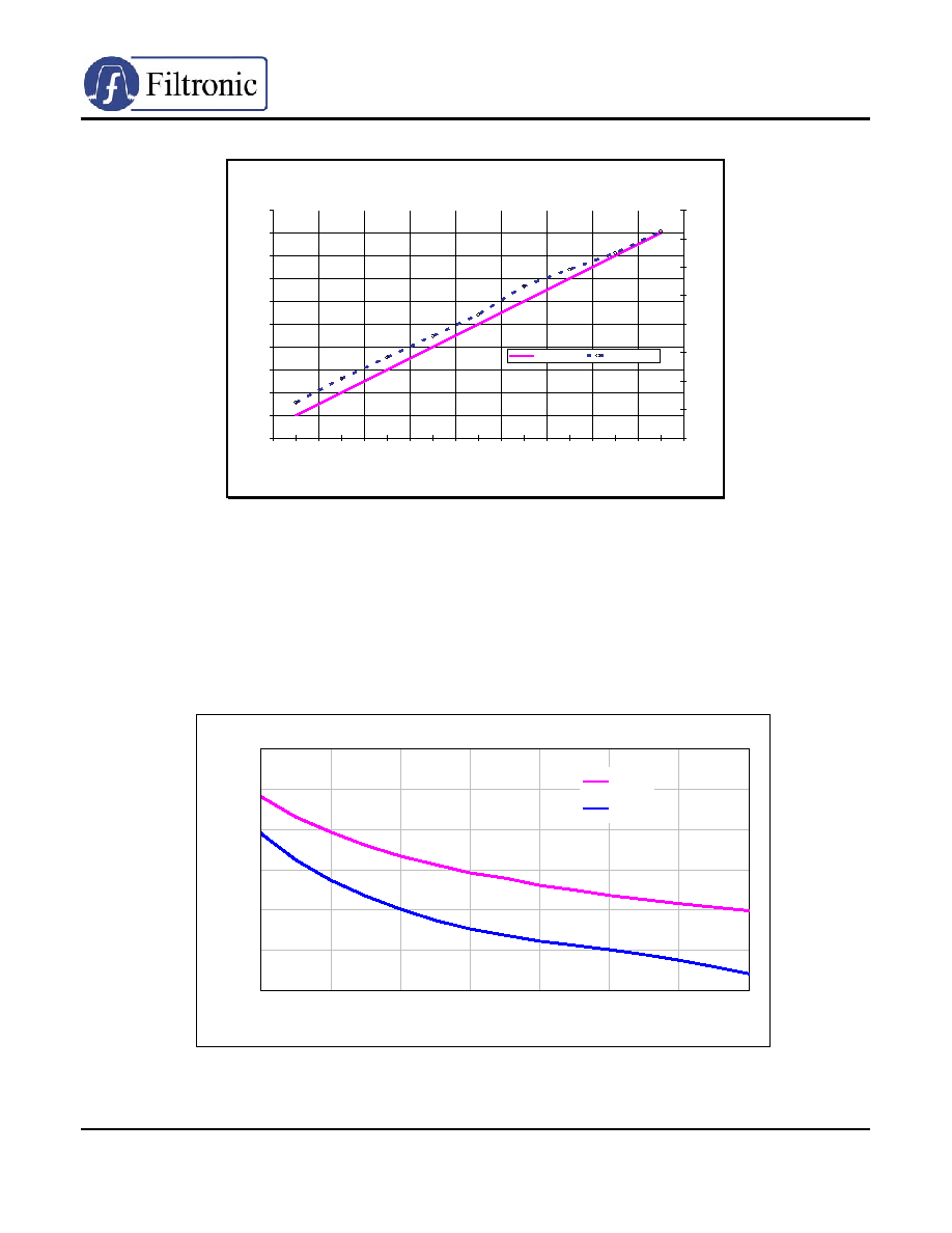
Note: pHEMT devices exhibit non-classical intermodulation performance, with equivalent IP3 values
exceeding 14 dB above P
1dB
. This IMD enhancement is affected by the quiescent bias current, the
Drain-Source voltage, and the tuning or matching applied to the device.
Maximum Stable Gain & S
21
Typical Intermodulation Performance
VDS =5V IDS = 50% IDSS at f = 1.85 GHz
10.0
11.0
12.0
13.0
14.0
15.0
16.0
17.0
18.0
19.0
20.0
-2.5
-1.5
-0.5
0.6
1.6
2.6
3.6
4.6
Input Power (dBm)
Out
put
P
o
wer
(
d
B
m
)
-60
-58
-56
-54
-52
-50
-48
-46
-44
3rd Order I
M
Product
s
(
d
B
c
)
Pout (dBm)
3rds (dBc)
1
2
3
4
5
6
7
8
Frequency (GHz)
FPD2250SOT89 5V / 50%IDSS
0
5
10
15
20
25
30
Ga
i
n
MSG
S21