
FPD7612
G
ENERAL
P
URPOSE P
HEMT
Phone: +1 408 850-5790
http://www.filtronic.co.uk/semis
Revised: 11/17/04
Fax: +1 408 850-5766
Email: sales@filcsi.com
∑
FEATURES
19 dBm Linear Output Power at 12 GHz
12 dB Power Gain at 12 GHz
17 dB Maximum Stable Gain at 12 GHz
11 dB Maximum Stable Gain at 18 GHz
45% Power-Added Efficiency
∑
DESCRIPTION AND APPLICATIONS
The FPD7612 is an AlGaAs/InGaAs pseudomorphic High Electron Mobility Transistor (PHEMT),
featuring a 0.25
µm by 200 µm Schottky barrier gate, defined by high-resolution stepper-based
photolithography. The recessed and offset Gate structure minimizes parasitics to optimize
performance. The epitaxial structure and processing have been optimized for reliable medium-
power applications. The FPD7612 also features Si
3
N
4
passivation and is available in a low cost
plastic package.
Typical applications include commercial and other narrowband and broadband high-performance
amplifiers, including SATCOM uplink transmitters, PCS/Cellular low-voltage high-efficiency output
amplifiers, and medium-haul digital radio transmitters.
∑
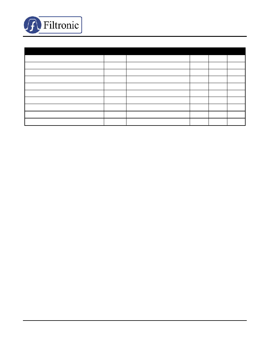
ELECTRICAL SPECIFICATIONS AT 22∞C
Parameter
Symbol
Test Conditions
Min
Typ
Max
Units
RF SPECIFICATIONS MEASURED AT f = 12 GHz USING CW SIGNAL
Power at 1dB Gain Compression
P
1dB
V
DS
= 5 V; I
DS
= 50% I
DSS
18
19
dBm
Power Gain at P
1dB
G
1dB
V
DS
= 5 V; I
DS
= 50% I
DSS
10.5
12.0 dB
Power-Added Efficiency
PAE
V
DS
= 5V; I
DS
= 50% I
DSS
;
P
OUT
= P
1dB
45 %
Maximum Stable Gain (S
21
/S
12
)
f = 12 GHz
f = 24 GHz
SSG
V
DS
= 5 V; I
DS
= 50% I
DSS
16
9.5
17
11
dB
Saturated Drain-Source Current
I
DSS
V
DS
= 1.3 V; V
GS
= 0 V
45
60
75
mA
Maximum Drain-Source Current
I
MAX
V
DS
= 1.3 V; V
GS
+1 V
120 mA
Transconductance G
M
V
DS
= 1.3 V; V
GS
= 0 V
80
mS
Gate-Source Leakage Current
I
GSO
V
GS
= -5 V
1
10
µA
Pinch-Off Voltage
|V
P
| V
DS
= 1.3 V; I
DS
= 0.2 mA
0.7
1.0
1.3
V
Gate-Source Breakdown Voltage
|V
BDGS
| I
GS
= 0.2 mA
12.0
14.0
V
Gate-Drain Breakdown Voltage
|V
BDGD
| I
GD
= 0.2 mA
14.5
16.0
V
Thermal Resistivity (see Notes)
JC
V
DS
> 3V
280
∞C/W
DRAIN
BOND
PAD (2X)
SOURCE
BOND
PAD (2x)
GATE
BOND
PAD (2X)
DIE SIZE (
µm): 520 x 400
DIE THICKNESS: 75
µm
BONDING PADS (
µm): >48 x 48
FPD7612
G
ENERAL
P
URPOSE P
HEMT
Phone: +1 408 850-5790
http://www.filtronic.co.uk/semis
Revised: 11/17/04
Fax: +1 408 850-5766
Email: sales@filcsi.com
∑
ABSOLUTE MAXIMUM RATINGS
1
Parameter
Symbol
Test Conditions
Min
Max
Units
Drain-Source Voltage
V
DS
-3V < V
GS
< +0V
8
V
Gate-Source Voltage
V
GS
0V < V
DS
< +8V
-3
V
Drain-Source Current
I
DS
For V
DS
> 2V
I
DSS
mA
Gate Current
I
G
Forward or reverse current
10
mA
RF Input Power
2
P
IN
Under any acceptable bias state
100
mW
Channel Operating Temperature
T
CH
Under any acceptable bias state
175
∫C
Storage Temperature
T
STG
Non-Operating Storage
-40
150
∫C
Total Power Dissipation
P
TOT
See De-Rating Note below
0.5
W
Gain Compression
Comp.
Under any bias conditions
5
dB
Simultaneous Combination of Limits
3
2 or more Max. Limits
80
%
1
T
Ambient
= 22
∞C unless otherwise noted
2
Max. RF Input Limit must be further limited if input VSWR > 2.5:1
3
Users should avoid exceeding 80% of 2 or more Limits simultaneously
Notes:
∑ Operating conditions that exceed the Absolute Maximum Ratings could result in permanent damage to the device.
∑ Thermal Resitivity specification assumes a Au/Sn eutectic die attach onto a Au-plated copper heatsink or rib.
∑ Power Dissipation defined as: P
TOT
(P
DC
+ P
IN
) ≠ P
OUT
, where
P
DC
: DC Bias Power
P
IN
: RF Input Power
P
OUT
: RF Output Power
∑ Absolute Maximum Power Dissipation to be de-rated as follows above 22∞C:
P
TOT
= 500mW ≠ (3.6mW/
∞C) x T
HS
where T
HS
= heatsink or ambient temperature.
Example: For a 85
∞C heatsink temperature: P
TOT
= 0.5W ≠ (0.0036 x (85 ≠ 22)) = 0.27W
∑
HANDLING PRECAUTIONS
To avoid damage to the devices care should be exercised during handling. Proper Electrostatic
Discharge (ESD) precautions should be observed at all stages of storage, handling, assembly, and
testing. These devices should be treated as Class 1A per ESD-STM5.1-1998, Human Body Model.
Further information on ESD control measures can be found in MIL-STD-1686 and MIL-HDBK-263.
∑
ASSEMBLY INSTRUCTIONS
The recommended die attach is gold/tin eutectic solder under a nitrogen atmosphere. Stage
temperature should be 280-290
∞C; maximum time at temperature is one minute. The recommended
wire bond method is thermo-compression wedge bonding with 0.7 or 1.0 mil (0.018 or 0.025 mm)
gold wire. Stage temperature should be 250-260
∞C.
∑
APPLICATIONS NOTES & DESIGN DATA
Applications Notes are available from your local Filtronic Sales Representative or directly from the
factory. Complete design data, including S-parameters, noise data, and large-signal models are
available on the Filtronic web site.
All information and specifications are subject to change without notice.