CONFIDENTIAL
EK7307 Objective DATA SHEET

CONFIDENTIAL
Microelectronics, Inc.
EK7307
OBJECTIVE
DATA SHEET
240-Output TFT Gate Driver IC
Eureka
6F, NO.12, INNOVATION 1
ST
. RD.,
SCIENCE-BASED INDUSTRIAL PARK,
HSIN-CHU CITY, TAIWAN, R.O.C.
TEL
886-3-5799255
FAX
886-3-5799253

CONFIDENTIAL
EUREKA
Objective-EK7307
- 1 -
Rev 0.1 Oct.17.2002
240- Output TFT Gate Driver IC
DESCRIPTION
The EK7307 is a 240-output TFT gate driver IC suitable
for driving large/medium scale of TFT LCD panels. The
special, COG and COF compatible, pad layout allows
direct mounting on the glass. The logic inputs, the logic
outputs and the power supply pins are available on both
sides and suitable for connecting multiple chips using the
on chip connection as signal path.
FEATURES
Output channels:
240 outputs
Driver operating frequency:
max. 1.2MHz
LCD supply voltage:
max. VEE+43V
Driver output levels:
two
Driver "L" level is changeable
Incorporates bi-directional shift register.
Supports multi chip operation via output pins.
Pulse width modulation function.
COG and COF compatible pad layout
Power and logic I/O pins on both sides
Through Chip connection
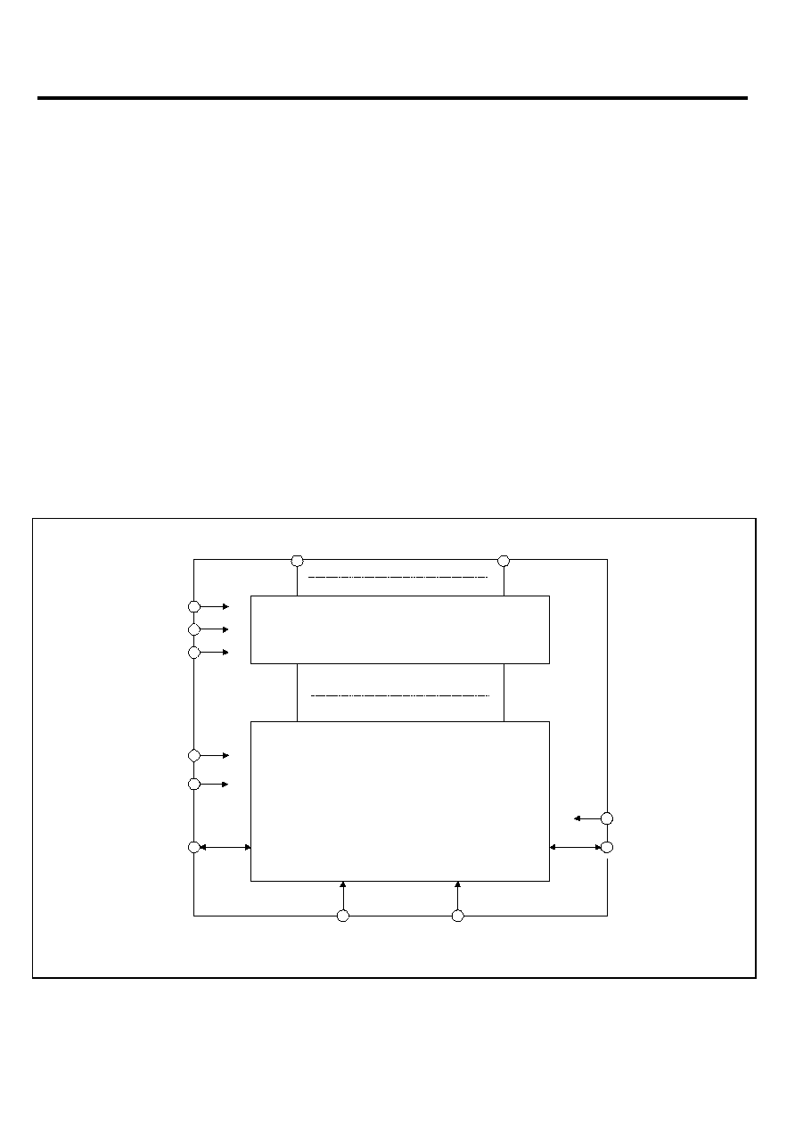
BLOCK DIAGRAM
High voltage output and level shifters
Low voltage logic and IO
V
G H
V
G L
V
E E
V
D D
V
S S
S T V 1
O E
S T V 2
C P V
L R
O U T 1
O U T 2 4 0
Fig. 1 Block diagram

CONFIDENTIAL
EUREKA
Objective -EK7307
- 2 -
Rev 0.1 Oct.17.2002
PINNING INFORMATION
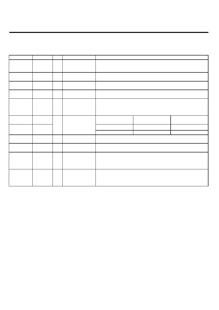
Table 1. Pad description
PAD Nr.
SYMBOL
I/O
Function DESCRIPTION
53 to 292
OUT
1
- OUT
240
O
TFT gate driver
output
Under the control of the shift register data, OE, and STV1 or STV2,
the driver outputs are V
GH
or V
GL
and change their value at the rising
edge of CPV
13 to 18,
327 to 332
V
GL
Supply
Power supply for TFT driver output low level
7 t0 12,
333 to 338,
V
EE
Supply
Negative power supply for Level shifters. Chip ground
346 to 349,
467 to 470
V
SS
Supply
Logic ground, Reference of the voltages
31 to 33,
38 to 41,
304 to 307
312 to 314
LR I
Shift direction
selection signal
LR = "H" : OUT1
OUT240 (Shift left)
LR = "L" : OUT240
OUT1 (Shift right)
25 to 27
318 to 320
STV1
STV1 STV2
LR = "H"
Input
Output
28 to 30
315 to 317
STV2
I/O
Start pulse input
and output
LR = "L"
Output
Input
34 to 37
308 to 311
CPV I
Shift register clock
input
The start pulse is sampled at the rising edge of CPV,
The carry pulse changes at the falling edge of CPV.
42 to 45
300 to 303
OE I
Negative active
input pin
When OE = "H" then the outputs are set to V
GL
independent of the
register data. This function is not synchronized with CPV.
1 to 6
339 to 344
350 to 355
461 to 466
V
DD
Supply
Logic positive power
19 to 24
321 to 326
356 to 361
455 to 460
V
GH
Supply
High voltage power and TFT driver output high level

CONFIDENTIAL
EUREKA
Objective -EK7307
- 3 -
Rev 0.1 Oct.17.2002
FUNCTIONAL DESCRIPTION
Power supplies
The TFT voltage, V
GL
and V
EE
, relative to the logic ground, can be a negative voltage value.
The TFT gate driver pins are either V
GL
or V
GH
.
V
G H
V
DD
V
S S
V
G L
V
E E
Fig. 2 Relative position of the different supply voltages
Shift direction
The input signals OE and the shift data control the value of the outputs (OUT
1
till OUT
240
). Their value can be either V
GH
or
V
GL
.
The signal LR controls the shift direction of the shift register. The shift register takes its value from one of the input/output
pins STV at the rising edge of the clock CPV and shifts the value to the other input/output pin STV where it is presented at
the falling edge of CPV.
Table 2. LR shift direction relation
LR
Start pulse taken from:
Data shift direction
Output pulse given at:
LR="H" STV1
OUT
1
OUT
240
STV2
LR="L"
STV2
OUT
240
OUT
1
STV1
