CONFIDENTIAL
Eureka Microelectronics, Inc.
EK7309
256-Outputs Gate Driver
6F, NO.12, INNOVATION 1
ST
. RD.,
SCIENCE-BASED INDUSTRIAL PARK,
HSIN-CHU CITY, TAIWAN, R.O.C.
http://www.eureka.com.tw

CONFIDENTIAL
EUREKA
EK7309
Contents
Page
1.GENERALDESCRIPTION
........................................................................
1
2.FEATURES
...........................................................................................
1
3.BLOCK DIAGRAM
..................................................................................
1
4.PIN CONFIGURATION
............................................................................
2
5.PIN FUNCTION DESCRIPTIONS
......................................................... ......
3
6.FUNCTION OPERATIONS
........................................................................
4
6.1
Power supply's
6.2
Shift direction
6.3
OE function
6.4 XDON function
7.TIMING DIAGRAM
.............................................................................. ...
5
8.ABSOLUTE MAXIMUM RATINGS
....................................... ............
......
7
8.1 Absolute maximum ratings
8.2 Recommended operating conditions
9. DC ELECTRICAL CHARACTERISTICS
...............
.....................................
8
9.1
Supply current
9.2
Input pin
9.3
I/O pin
9.4
Output pin
10. AC ELECTRICAL CHARACTERISTICS
...
...............................................
10

CONFIDENTIAL
TFT Gate Driver (256 Outputs)
3.
BLOCK DIAGRAM
1.
GENERAL DESCRIPTION
EUREKA
EK7309
2.
FEATURES
May 2003 -01-
Preliminary Rev 0.2
EK7309
is a TFT LCD gate driver with 256 outputs
for XGA/SXGA display systems. The logic and
control portion is implemented in standard CMOS
circuits while the output drivers use high voltage
CMOS design. The low voltage part includes a 256-
stage bidirectional shift register with right and left
shift I/O for cascading. The output of the shift register
is then level translated to drive the high voltage
output buffer. There are four supply voltages for
EK7309
. VDD/VSS are the supply voltages for logic
interfaces. Typically VDD is at 3.3V while VSS is 0V.
VGG and VEE are the supply voltages for the
output driver. VEE is the most negative supply
voltage for the internal substrate of
EK7309
.
EK7309
allows three output enable controls (OE1-
3) and one global enable signal (XON).
� 256 gate drive outputs
� Bidirectional shift control and cascadable
� Output enable and global on control
� Maximum shift clock frequency up to 100KHz
� 3.3V CMOS logic I/O
� High voltage output drive
� Operating supply range
Logic (VDD-VSS: 3.3V)
Output Drive (VGG -VEE: 40V)
� TCP package
High voltage output and level shifters
Low voltage logic and IO
V
GG
V
EE
V
DD
V
SS
DIO1
OE1
DIO2
SCLK
RL
X
1
X
256
XON
OE2
OE3
CONFIDENTIAL
EUREKA
EK7309
May 2003 -02-
Preliminary Rev 0.2
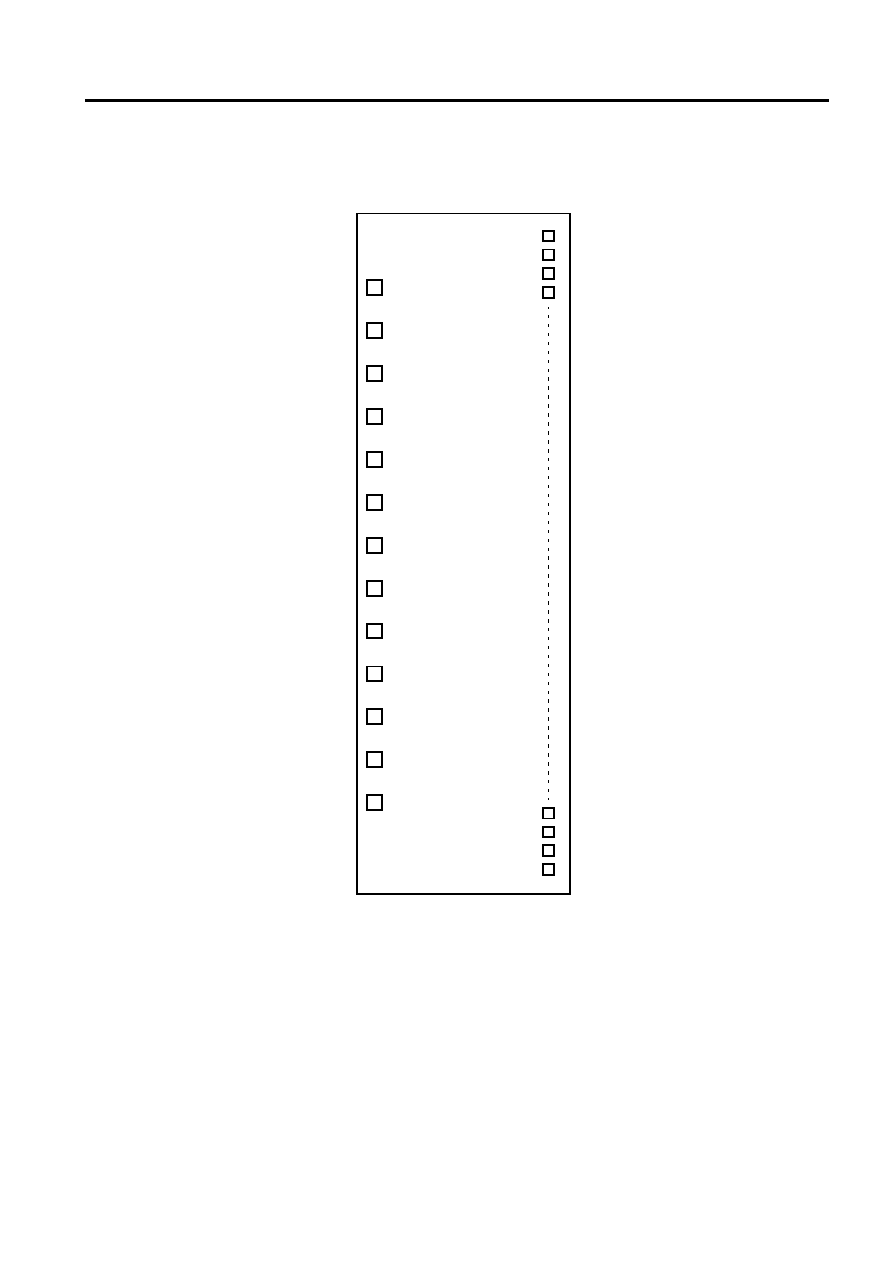
4.
PIN
CONFIGURATION
Figure-1
IC top view. This diagram shows
EK7309
's pin configuration only. It does not
necessarily correspond to the pad layout on the chip.
VEE
VEE
VSS
DIO1
XON
RL
SCLK
OE1
OE2
OE3
DIO2
VDD
VGG
X1
X2
X3
X4
X253
X254
X255
X256
EK73
0
9