 | –≠–ª–µ–∫—Ç—Ä–æ–Ω–Ω—ã–π –∫–æ–º–ø–æ–Ω–µ–Ω—Ç: EK7601 | –°–∫–∞—á–∞—Ç—å:  PDF PDF  ZIP ZIP |

CONFIDENTIAL
DOC NO
TDS760 -0
REV
.0
DOC Title
EK7601 Data Sheet
Page
/
/
Revision History
REV.
REV Date
Eff. Date
REV. Page
/
/
Revise item / Content
.0
2002/02/2
2002/3/5

CONFIDENTIAL
Microelectronics, Inc.
EK7601
240-Channel Analogue Source
Driver for colour TFT LCDs
Eureka
Eureka
Eureka
Eureka
6F, NO.12, INNOVATION 1
ST
. RD., SCIENCE-BASED
INDUSTRIAL PARK, HSIN-CHU CITY, TAIWAN, R.O.C.
TEL
886-3-5799255
FAX
886-3-5799253
http://www.eureka.com.tw

CONFIDENTIAL
EUREKA
EK7601
- 2 -
Rev 1.0 Feb.21.2002
240-Channel Analogue Source Driver
for colour TFT LCDs
OVERVIEW
The EM7601 is an analogue, fully colour, source driver for TFT LCD panels designed for camera,
TV etc. Analogue R, G and B signal are applied directly on the chip. For each of the 240 outputs,
the voltage is sampled and buffered to the panel. With a double sample and hold circuit a new
voltage can be sample whereas the previous sample voltage is applied to the panel.
According to different modes, the 3 input voltages (VA, VB, VC) can be applied on different output
to support various pixel array types.
The 3 input voltages (VA, VB, VC) can be sampled simultaneously or sequentially to have a
better flexibility with the input voltage. Using enable signal (STHx), several chips can be
cascaded for large panel.
FEATURE
∑
LCD outputs: 240
∑
Bi-directional shift (L/R)
∑
Simultaneous or Sequential RGB acquisition mode
∑
X1 or X3 clock mode
∑
High frequency Sampling 10MHz (x1)
∑
Automatic low power consumption mode after data capture (gated clock)
∑
RGB colour selection (automatic or manual)
∑
Applicable to COG / COF
∑
Logic power supply voltage V
DD
: 2.7V ≠ 5.25V
∑
LCD power supply voltage AV
DD
: 4.5V ≠ 5.5V
∑
Output dynamic range AV
SS
+0.2V to AV
DD
-0.2V
∑
Applicable to COG/COF
CONFIDENTIAL
EUREKA
EK7601
- 3 -
Rev 1.0 Feb.21.2002
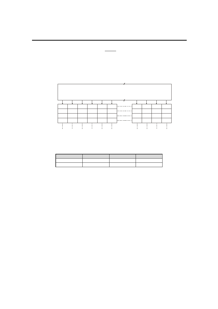
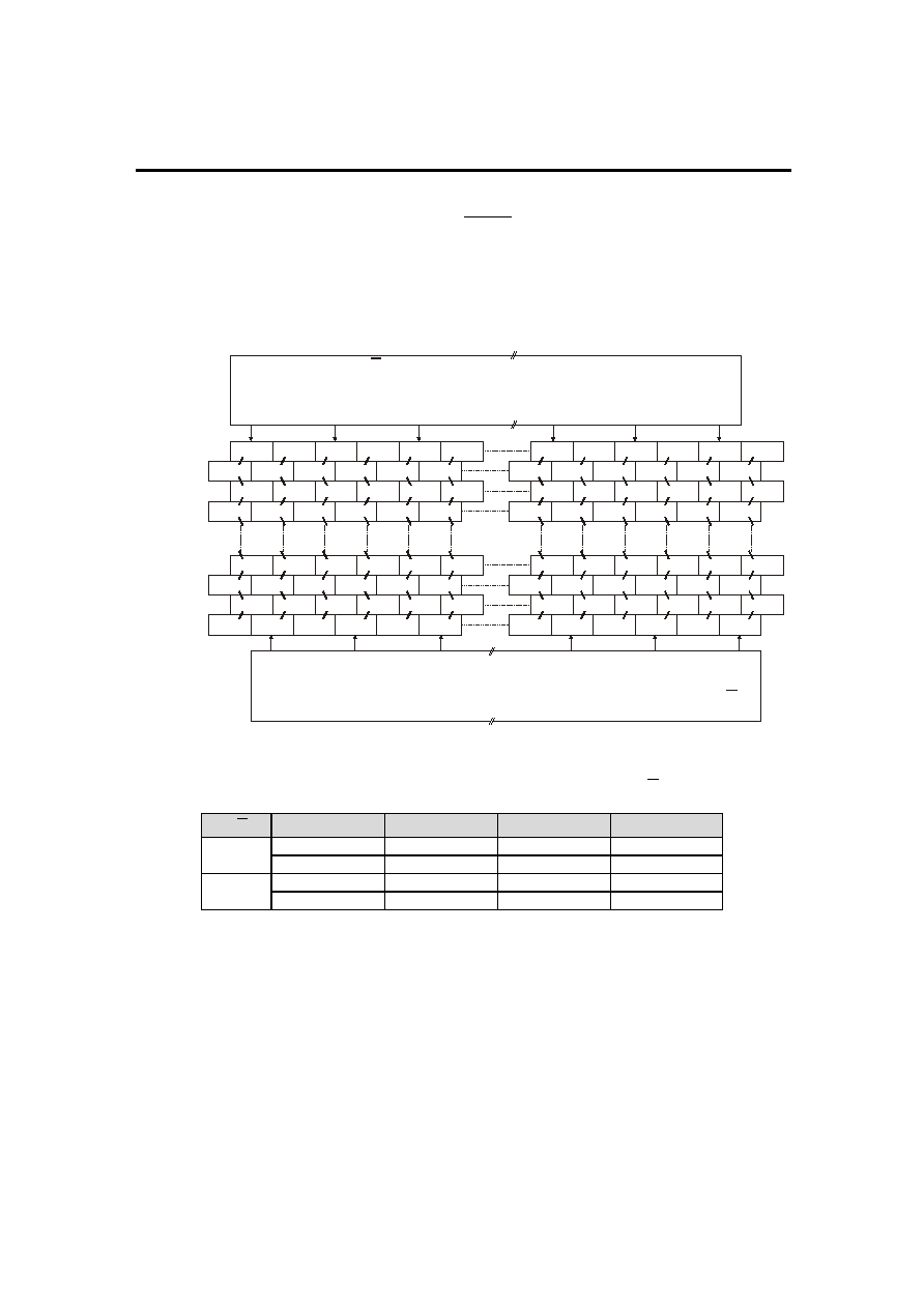
1. INTERNAL
BLOCK
DIAGRAM
MODE
-
+
SHA SHB
AM
U
X
AM
U
X
MU
X
SR
-
+
SHA SHB
AM
U
X
MU
X
SR
-
+
SHA SHB
AM
U
X
MU
X
SR
-
+
SHA SHB
AM
U
X
MU
X
SR
-
+
SHA SHB
AM
U
X
MU
X
SR
-
+
SHA SHB
AM
U
X
MU
X
SR
-
+
SHA SHB
AM
U
X
MU
X
SR
VA (R)
CPH1
VB (G)
VC (B)
CPH3
STH1
STH2
Q1H
INH
Q2H
TEST2
L/R
Li
ne
C
ont
r
o
l
Clock
MUX
QA1
QA80
QA2
QB1
QB80
QC1
QC80
Figure 1.1:
Block diagram
1. Clock MUX
Selects if the sampling is simultaneous or sequential and the clocks are divided by three
or not. Also gates the clock.
2. 3 x 80-bit bi-directional shift register
Generates enable signals for sequential sampling 80 groups of 3 input colours.
3. Line
control
Select sample circuit SHA or SHB and the high impedance output state
4. SH control MUX
Select which sample and hold circuit samples the analogue input value.
5. RGB
MUX
According to the controls signals, selects which input colour goes to which group of
outputs.
6. Sample and hold Circuit (SHA, SHB)
Sample the input voltage when the enable signal of the shift register is generated and
hold this value until it is stored on the panel.
7. Buffers
Drive the sample greyscale voltage on the panel.
CONFIDENTIAL
EUREKA
EK7601
- 4 -
Rev 1.0 Feb.21.2002
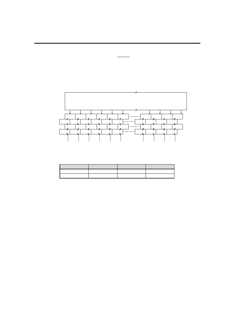
2. PIN CONFIGURATION (COF PACKAGE)
Copper
Foil
Surface
RESET
MODE
INH
STH1
CPH3
CPH2
CPH1
VDD
AVDD
VSS
COM
COM
NC
STH2
COM
COM
TEST2
Q2H
COM
COM
AVSS
Q1H
COM
COM
VC
L/R
VB
VA
COM
COM
Qa
1
Qb
1
Qc
1
COM
COM
COM
COM
Qa
80
COM
COM
Qb
80
COM
COM
Qc
80
COM
COM
Figure 2.1:
Pin Arrangement
CONFIDENTIAL
EUREKA
EK7601
- 5 -
Rev 1.0 Feb.21.2002
3. PIN
FUNCTION
DESCRIPTION
Signal Name
Pin Type
Function
Qa1 to Qa80
Qb1 to Qb80
Qc1 to Qc80
Output
Liquid-crystal application voltages
Each QaX, QbX or QcX correspond to one of the analogue
sample input signal VA, VB or VC.
VA
VB
VC
Input
Video input signal
Analogue video input signal that is sampled internally and
applied to the panel.
R
L/
Input
Controls the display data shift direction
L/R = H : STH1 input, Qa1
Qc80, STH2 output.
L/R = L : STH2 input, Qc80
Qa1, STH1 output.
STH1
Bidir
Right shift start pulse
L/R = H : Becomes the start pulse input pin
L/R = L : Becomes the start pulse output pin
STH2
Bidir
Left shift start pulse
L/R = H : Becomes the start pulse output pin
L/R = L : Becomes the start pulse input pin
CPH1
CPH2
CPH3
Input
(Pull-down
CPH2 & CPH3
@ TEST2 = L
And MODE=H)
Sampling clock input
Refers to the analogue data-sampling clock. The sampling
starts at the first rising edge of CPH1 when STH1 (L/R=H) is
activated.
CPH1 can be internally divided (x3 mode) to generate internal
clock signal CPH1'.
The sampling can be simultaneous or sequential.
In simultaneous mode, the sampling is made during CPH1
(CPH1') period for all output.
In sequential mode, the sampling is made according the table
below:
CPH1 (CPH1') control the sampling for Qa1
Qa80
CPH2 (CPH2') control the sampling for Qb1
Qb80
CPH3 (CPH3)' control the sampling for Qc1
Qc80
When clock mode x1 and sequential is selected, the three
inputs CPH1, CPH2 and CPH3 must have an input clock signal
applied. Otherwise only CPH1 must have input clock applied.
The clock selection table was described on the page 8.
INH
Input Load
line
The sampled voltages are connecting to the panel at the rising
edge of INH. The outputs of SHA(B) that was in sample mode
are applied to the panel, whereas the SHB(A) becomes ready
to sample new values.
During INH = L, output level is HiZ state and this signal initialise
the internal circuits.
CONFIDENTIAL
EUREKA
EK7601
- 6 -
Rev 1.0 Feb.21.2002
TEST2
Input
(Pull-up)
Input signal colour rotation mode selector
TEST2 = L: No data rotation mode.
Input voltage of each output QaX, QbX and QcX are selected
from VA, VB and VC according to the control signal Q1H and
Q2H.
Simultaneous or sequential clock mode is selected by MODE.
TEST2= H or open: Automatic rotation mode.
Input voltage of each output QaX, QbX and QcX are selected
automatically from VA, VB and VC according to the filter arrays,
selected by the control signal Q1H and Q2H.
Simultaneous or sequential clock mode is selected by Q1H,
Q2H.
MODE
Input
(Pull-down
@ TEST2 = L)
Sampling mode selection
MODE = L or open: Sequentially sampling
MODE = H: Simultaneous sampling
This signal is only usable when TEST2= L.
Q1H
Q2H
Input
(Pull-down
@ TEST2 = L)
Colour selection input
When TEST2 = L: Q1H and Q2H select which input voltage
(VA, VB, VC) correspond to QaX, QbX, QcX outputs.
When TEST2 =H: Q1H and Q2H select the filters array colours
sequence. Q1H and Q2H select also simultaneous/sequential
mode according to the equation below.
Q1H = Q2H = 0: Simultaneous sampling
Q1H =1 OR Q2H = 1: Sequential sampling
The colour selection table and filter array are describe on page
12.
RESET
Input
(Pull-down
@ TEST2 = L)
Automatic colour selection Initialisation
Reset the system of the automatic rotation mode. To initialise
the module a pulse on INH must be applied after reset.
This function is only usable when TEST2=H. When not used
should be L or open.
V
DD
Power
Logic part power supply
V
SS
Power Logic
part
ground
AV
DD
Power
Analogue part power supply
AV
SS
Power
Analogue part ground
CONFIDENTIAL
EUREKA
EK7601
- 7 -
Rev 1.0 Feb.21.2002
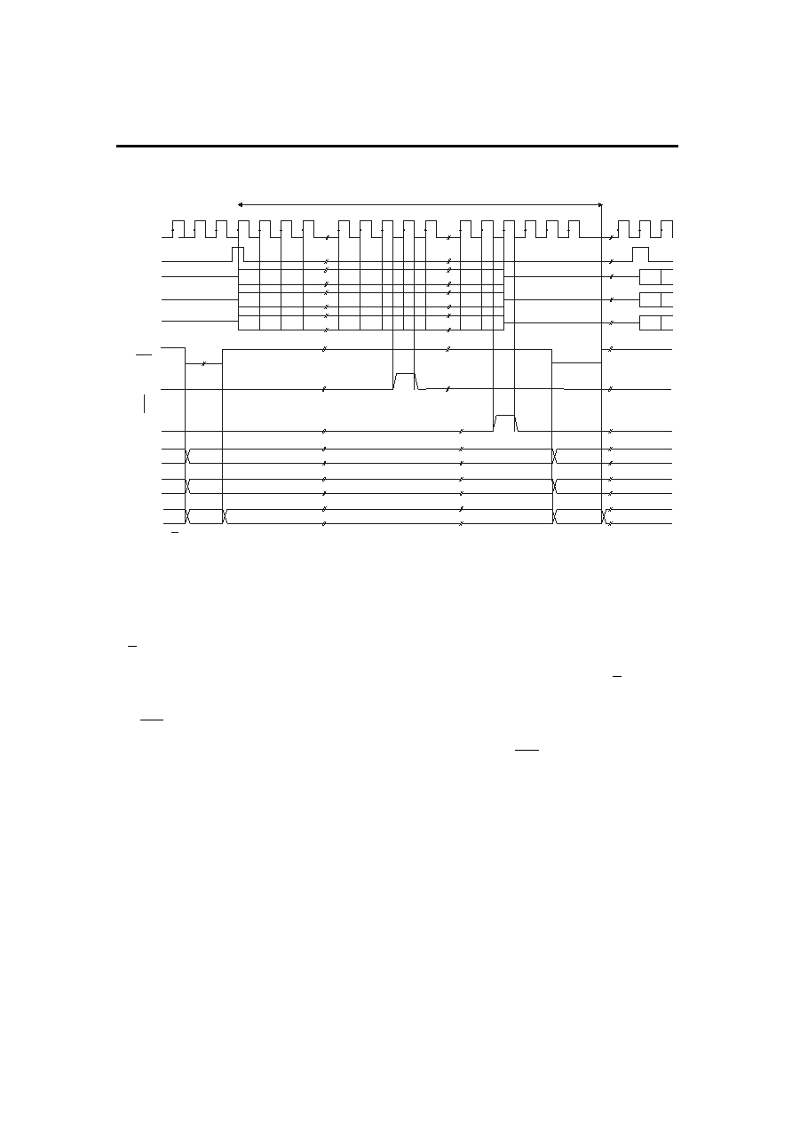
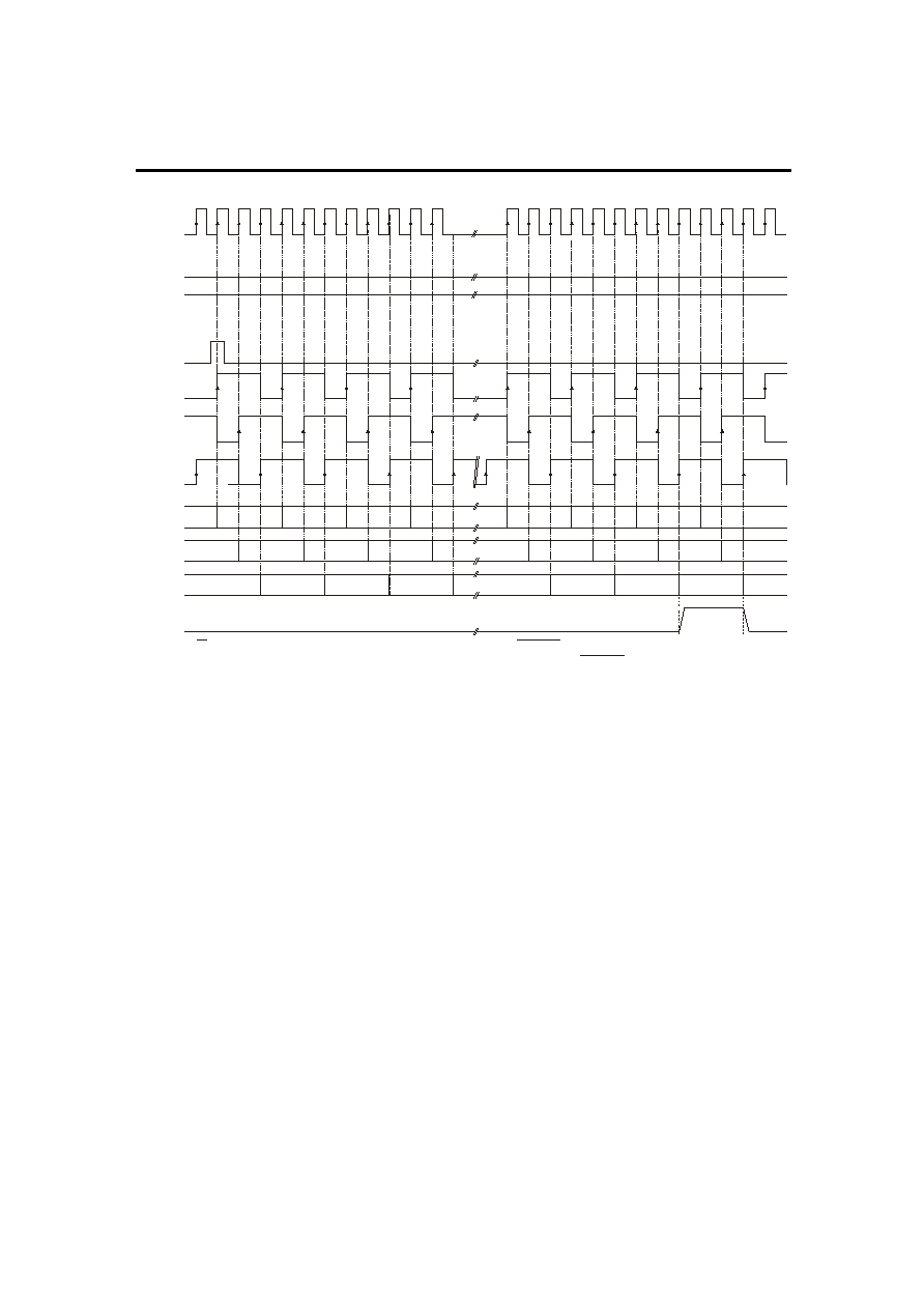
4. OPERATION
TIMING
CPH1
STH1
VA
VB
VC
INH
STH2
1 Chip
st
STH2
Last Chip
Buffers
Ouputs
Drivers
Outputs
L/ = H shift from left to right
Clock mode : x1 simultaneous
R
No rotation mode
VA -> QAx
VB -> QBx
VC -> QCx
Ax, Bx, Cx correspond to the
sample values for the
outputs QAx, QBx, QCx.
A1
B1
C1
A78
B78
C78
A79
B79
C79
A319
B319
C319
A80
B80
C80
A320
B320
C320
A81
B81
C81
A2
B2
C2
A3
B3
C3
Line n-1
Line n-1
High Z
High Z
Line n
Line n
1
78
319
2
1
82
79
320
3
80
321
4
81
Line
Sample
circuits
SHA Line n
SHB Line n+1
A1
B1
C1
2
Figure 4.1:
Operation timing diagram
The start condition is initiated by applying a start pulse to the enable input pin (STH1 when
L/R=VDD) at the beginning of each line on the first chip. During the next 80 CPH1 rising edges,
this source driver sample 80 times 3 display input voltage (3 RGB dot x 80 pixels). After sampling
the 80
th
group of input voltages, it activates the enable output signal (STH2 when L/R=VDD) to
enable the following chip.
As soon as the loading of the input voltage is achieved for a complete line, the controller activates
the INH signal to force the 240 output buffers in a high impedance state. Then the outputs of
SHA(B) that were in sample mode are applied to the output buffers , whereas the SHB(A)
becomes ready to sample new values. Finally, at the rising edge of INH, the 240 output buffers
drive the sample voltages to the panel.
CONFIDENTIAL
EUREKA
EK7601
- 8 -
Rev 1.0 Feb.21.2002
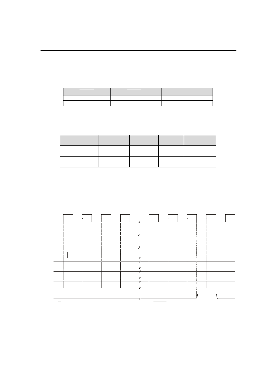
5. SAMPLING
MODES
Simultaneous/Sequential and x1/x3 sampling modes provide 4 different ways to sample input
voltages.
Simultaneous/Sequential selection mode is described on the table below.
When TEST2 =L
When TEST2 =H
Sampling Mode
Mode=H Q1H=Q2H=L
Simultaneous
Mode=L
Q1H=H OR Q2H =H
Sequential
Table 5.1:
Simultaneous Sequential selection table
Sampling Mode
CPH1
CPH2
CPH3
Clock
division
Simultaneous Clock
IN
L
L
Sequential
Clock IN
Clock IN
Clock IN
x1
Simultaneous Clock
IN
L
H
Sequential Clock
IN
L
H
x3
Table 5.2:
x1 x3 clock selection table
All diagram below describe the 4 clock modes, voltage correspondence are: VA -> QAX, VB ->
QBX, VC -> QCX.
Ax, Bx, Cx correspond to the sample values for the outputs QAx, QBx, QCx.
CPH3
CPH2
CPH1
STH1
VA
VB
VC
STH2
A1
B1
C1
A78
B78
C78
A79
B79
C79
A2
B2
C2
A3
B3
C3
1
78
2
79
3
4
A80
B80
C80
80
81
L/ = H shift from left to right
R
CPH2 = CPH3 = L
MODE = H when
= L OR
Q1H = Q2H = L when
= H
TEST2
TEST2
Figure 5.1:
x1 simultaneous sampling mode
Each input is sampled simultaneously synchronised with CPH1 rising edge.
Output enable signal is generated at the falling edge of the 80
th
period of CPH1 since the start
pulse.
CONFIDENTIAL
EUREKA
EK7601
- 9 -
Rev 1.0 Feb.21.2002
CPH3
CPH2
CPH1
STH1
VA
VB
VC
STH2
A1
B1
C1
A78
B78
C78
A79
B79
A2
B2
C2
A3
B3
C3
1
1
1
78
78
78
2
2
2
79
79
3
3
3
4
4
4
A80
B80
C80
79
80
80
80
81
81
81
C79
L/ = H shift from left to right
R
CPH2, CPH3 : clock input
MODE = L when
= L OR
Q1H = H or Q2H = H when
= H
TEST2
TEST2
Figure 5.2:
x1 sequential sampling mode
Each input is sampled sequentially synchronised with the associated rising edge of the
corresponding clock. CPH1 controls the sample for QAx outputs, CPH2 controls the sample for
QBx outputs and CPH3 controls the sample for QCx outputs.
Output enable signal is generated at the falling edge of the 80
th
period of CPH1 since the start
pulse.
CONFIDENTIAL
EUREKA
EK7601
- 10 -
Rev 1.0 Feb.21.2002
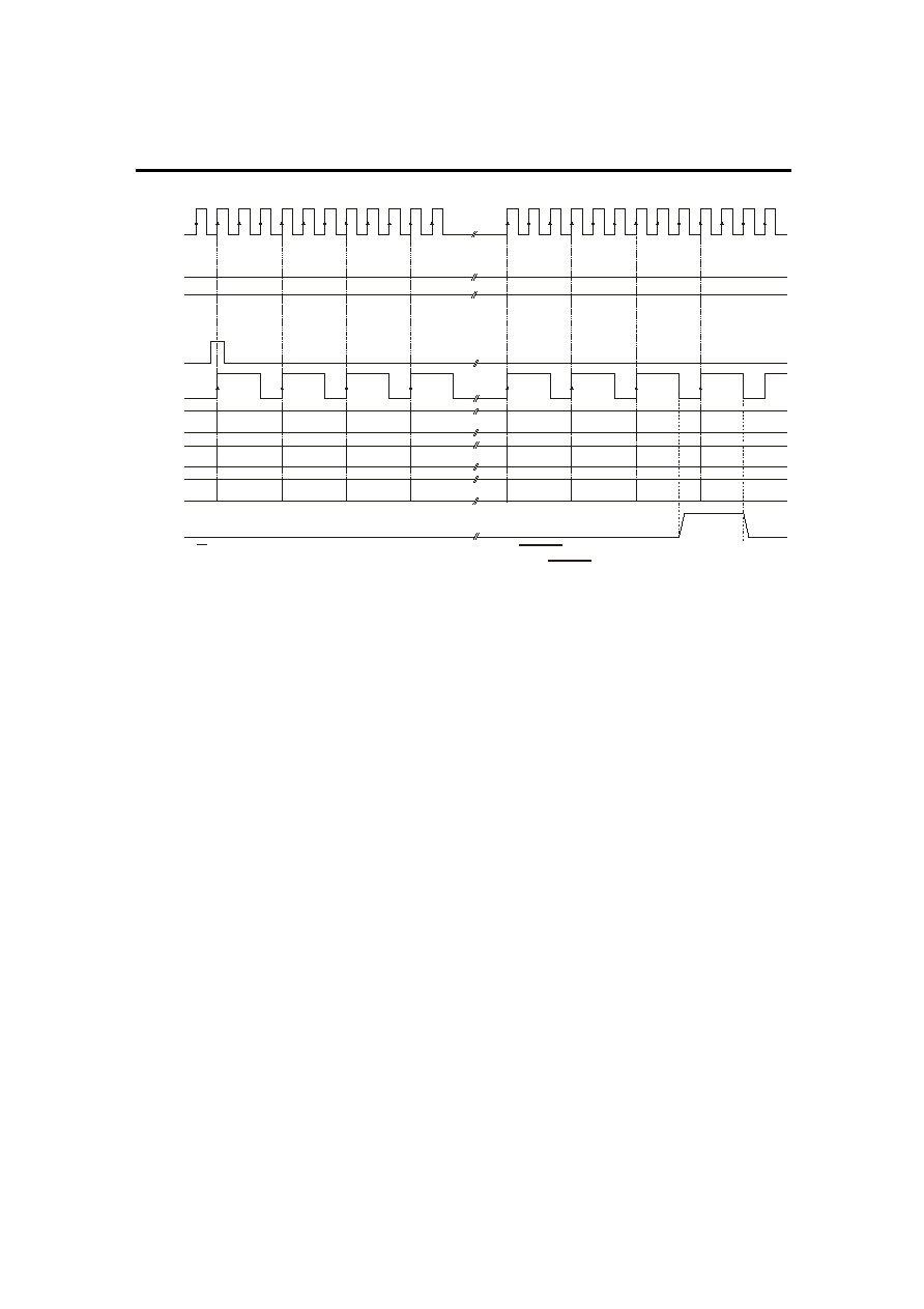
CPH3
CPH2
CPH1
STH1
VA
VB
VC
STH2
A1
B1
C1
A78
B78
C78
A79
B79
C79
A2
B2
C2
A3
B3
C3
1
2
3
4
5
6
7
8
9
10
11
A80
B80
C80
CPH1'
234 235 236 237 238 239 240 241 242 243 244 245
1
2
3
4
78
79
80
81
L/ = H shift from left to right
R
CPH2 = L CPH3 = H
MODE = H when
= L OR
Q1H = Q2H = L when
= H
TEST2
TEST2
Figure 5.3:
x3 simultaneous sampling mode
Each input is sampled simultaneously synchronised with CPH1' rising edge. CPH1' is generated
from CPH1 (Frequency divided by 3).
Output enable signal is generated at the falling edge of the 80
th
period of CPH1' since the start
pulse.
CONFIDENTIAL
EUREKA
EK7601
- 11 -
Rev 1.0 Feb.21.2002
CPH3'
CPH2'
VA
VB
VC
STH2
A1
B1
C1
A78
B78
C78
A79
B79
A2
B2
C2
A3
B3
C3
A80
B80
C80
C79
CPH3
CPH2
CPH1
STH1
1
1
1
1
234
2
235
3
236
4
5
237
6
238
7
239
8
240
9
241
10
242
11
243 244
78
2
2
2
79
3
3
3
4
4
4
80
81
CPH1'
78
79
80
81
78
79
80
81
L/ = H shift from left to right
CPH2 = L CPH3 = H
R
MODE = L when
= L OR
Q1H = H or Q2H = H when
= H
TEST2
TEST2
245
Figure 5.4:
x3 sequential sampling mode
Each input is sampled sequentially synchronised with the associated rising edge of the
corresponding clock. CPH1' controls the sample for QAx outputs, CPH2' controls the sample for
QBx outputs and CPH3' controls the sample for QCx outputs.
CPH1', CPH2' and CPH3' are generated from CPH1 (Frequency divided by 3). The three clocks
have one CPH1 period phase shift between them.
Output enable signal is generated at the falling edge of the 80
th
period of CPH1' since the start
pulse.
CONFIDENTIAL
EUREKA
EK7601
- 12 -
Rev 1.0 Feb.21.2002
6. COLOUR MODE SELECTION
According to the signal description table, the colour mode selection is separated in two modes.
No rotation mode and automatics rotation mode.
NO ROTATION MODE
This mode is selected by TEST2 = L. When no rotation mode is selected, Q1H and Q2H control
the colour selection in order to the table below.
Q1H
Q2H
QA
QB
QC
L L
VA
VB
VC
L H
VC
VA
VB
H X
VB
VC
VA
Table 6.1:
No rotation mode colour selection table
The sample circuit SHA(B) get the value according to the table above.
For example, when Q1H = Q2H = L, the sample circuit SHA(B) for the outputs Qax sample VA
and the next INH pulse this sample voltage is put to the panel.
AUTOMATIC ROTATION MODE
This mode is selected by TEST2 = H. It allows the chip to select automatically the colour in
function of the panel colour filter and the chips location on the panel (single bank or dual bank).
Single bank mean that all the source drivers are on one side of the panel. Dual bank means that
one group of source drivers is in the top of the panel and one at the bottom of the panel and they
drive columns alternatively.
Q1H
Q2H
Colour array
Chip location
L L
Vertical
Stripe
Single
bank
L H Delta Single
bank
H X Delta Dual
bank
Table 6.2:
Automatic rotation mode panel selection table
In this mode, the colour selection has a cycle of two lines. A pulse on RESET and after an
activation of INH initialises this sequence (figure below).
INH
1 line (Odd)
st
2 line (Even)
nd
1 line sampling
st
2 line sampling
nd
RESET
Sample
Q to Q
A1
C80
Figure 6.1:
Automatic rotation mode initialisation sequence
In automatic rotation mode, the colour is selected automatically for Odd and Even line.
CONFIDENTIAL
EUREKA
EK7601
- 13 -
Rev 1.0 Feb.21.2002
Vertical stripe array
This mode is selected by Q1H = Q2H = L and TEST2=H.
The characteristics of this panel configuration are:
∑
Each column is associated with one colour.
∑
One bank of source driver.
R(VA)
1 line
st
2 line
nd
3 line
rd
4 line
th
QA1
QA2
EK7601
QA80
QB1
QB2
QB80
QC1
QC79
QC2
QC80
G(VC)
B(VB)
R(VA)
G(VC)
B(VB)
R
R
R
R
R
G
G
G
G
G
G
G
B
B
B
B
B
R
R
R
R
R
G
G
G
G
G
G
G
B
B
B
B
B
Q1H = L Q2H = L
VA = R VB = B VC = G
Figure 6.2:
Vertical stripe array panel configuration
The figure shows, for this mode, that there is only one case of colour:
Line
QA
QB
QC
Odd VA VB VC
Even VA VB VC
Table 6.3:
Vertical stripe array colour selection table
CONFIDENTIAL
EUREKA
EK7601
- 14 -
Rev 1.0 Feb.21.2002
Single bank delta array
This mode is selected by Q1H = L, Q2H = H and TEST2 = H.
The characteristics of this panel configuration are:
∑
Each column is share between two colours.
∑
One bank of source driver.
R(VA)
1 line
st
2 line
nd
3 line
rd
4 line
th
G(VC)
B(VB)
B(VB)
R(VA)
G(VC)
R
R
R
R
R
G
G
G
G
G
G
G
B
B
B
B
B
B
B
B
B
B
R
R
R
R
R
R
R
G
G
G
G
G
Q1H = L Q2H = H
VA = R VB = B VC = G
QA1
QA2
EK7601
QA80
QB1
QB2
QB80
QC1
QC79
QC2
QC80
Figure 6.3:
Single bank delta array panel configuration
The colours are switched between Odd and Even line:
Line
QA
QB
QC
Odd VA VB VC
Even VB VC VA
Table 6.4:
Single bank delta array colour selection table
CONFIDENTIAL
EUREKA
EK7601
- 15 -
Rev 1.0 Feb.21.2002
Dual bank delta array
This mode is selected by Q1H = H, Q2H = H and TEST2 = H.
The characteristics of this panel configuration are:
∑
Each column is share between two colours.
∑
Two bank of source driver (top and bottom of the panel).
R(VB)
R(VB)
R(VB)
R(VB)
1 line
st
last-3 line
2 line
nd
last-2 line
3 line
rd
last-1 line
4 line
th
last line
G(VC)
G(VC)
G(VA)
G(VA)
B(VC)
B(VC)
B(VA)
B(VA)
B(VA)
B(VA)
B(VC)
B(VC)
R(VB)
R(VB)
R(VB)
R(VB)
G(VA)
G(VA)
G(VC)
G(VC)
R
R
R
R
R
R
R
R
R
R
R
R
G
G
G
G
G
G
G
G
G
G
G
G
B
B
B
B
B
B
B
B
B
B
B
B
B
B
B
B
B
B
B
B
B
B
B
B
R
R
R
R
R
R
R
R
R
R
R
R
G
G
G
G
G
G
G
G
G
G
G
G
QA1
QA1
EK7601
QA80
QA80
QB1
QC1
QB80
QB80
QB1
QC1
QC80
QC80
EK7601
Q1H = H Q2H = H L/ = L
VA = G VB = R VC = B
R
Q1H = H Q2H = H L/ = H
VA = B VB = R VC = G
R
Figure 6.4:
Dual bank delta array panel configuration
The colours are switched between Odd and Even line and depend also on L/R:
R
L/
Line
QA
QB
QC
Odd VB VC VA
H
Even VA VB VC
Odd VA VB VC
L
Even VB VC VA
Table 6.5:
Dual bank delta array colour selection table
CONFIDENTIAL
EUREKA
EK7601
- 16 -
Rev 1.0 Feb.21.2002
COLOURS SELECTION RESUMING TABLE
The table below resume 3 different colour cases:
Case
QA
QB
QC
1
VA VB VC
2
VC VA VB
3
VB VC VA
Table 6.6:
RGB Colour selection case
The table below resume all colour selection modes:
When TEST2 =H
Q1H
Q2H
LR
When
TEST2 =L
Odd line
Even line
L L X
1
1
1
L H X
2
1
3
H H L
3
1
3
H H H
3
3
1
Table 6.7:
Colours selection resuming table
The numbers represent the different colour cases are listed on Table 6.6.
7.
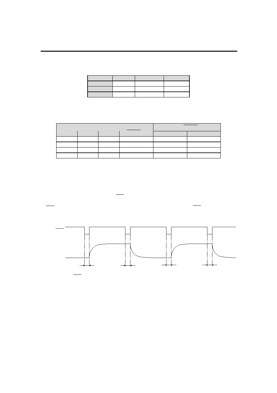
RELATIONSHIP BETWEEN INH AND OUTPUT WAVEFORM
At INH rising edge, the sample voltages are output on the panel. As long as INH is active, the 240
output buffers are forced in a high impedance state.
INH
Hi-Z
Hi-Z
Hi-Z
Hi-Z
Q to Q
A1
C80
Figure 7.1:
INH timing diagram
CONFIDENTIAL
EUREKA
EK7601
- 17 -
Rev 1.0 Feb.21.2002
OBJ
ECT
IVE
OBJ
ECT
IVE
8. ELECTRICAL
SPECIFICATION
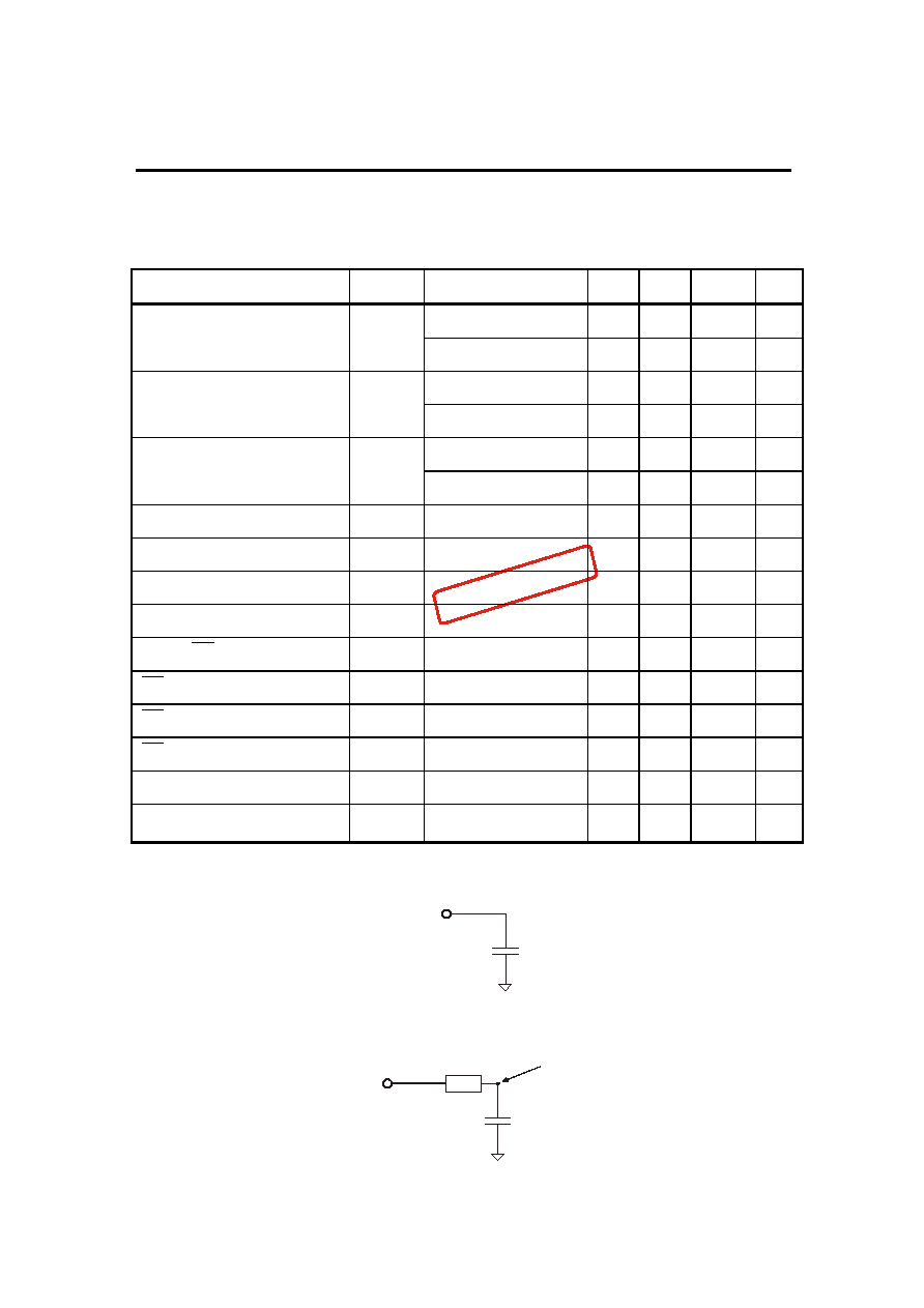
Absolute Maximum Rating (V
SS
= AV
SS
= 0 V)
Parameter Symbol
Rating
Unit
Logic Part Supply Voltage
V
DD
-0.5 to +7.0V
V
Analogue Part Supply Voltage
AV
DD
-0.5 to +7.0V
V
Logic Part Input Voltage
V
I1
-0.5 to VDD + 0.5
V
Video Input Voltage
V
I2
-0.5 to AVDD + 0.5
V
Logic Part Output Voltage
V
O1
-0.5 to VDD + 0.5
V
Driver Part Output Voltage
V
O2
-0.5 to AVDD + 0.5
V
Storage Temperature
T
STG
-55
to
+125
∞C
Caution: If the absolute maximum rating of even one of the above parameters is exceeded
even momentarily, the quality of the product may be degraded. Absolute
maximum rating, therefore, specify the values exceeding which the product may
be physically damaged. Be sure to use the product within the range of the
absolute maximum rating.
Recommended Operating Range (V
SS
= AV
SS
= 0 V)
Parameter Symbol
Conditions
MIN
TYP
MAX
Unit
Logic Part Supply Voltage
V
DD
2.7 5.25
V
Analogue Part Supply Voltage
AV
DD
4.5 5.5
V
Video Input Voltage
V
VIDEO
AV
SS
+ 0.2
AV
DD
- 0.2
V
Operating Ambient Temperature
T
A
-30
75
∞C
X1 Mode
10
MHz
Maximum Clock Frequency
F
CPH
X3 Mode
25
MHz
INH period
T
INH
64
200
µ
s
CONFIDENTIAL
EUREKA
EK7601
- 18 -
Rev 1.0 Feb.21.2002
OBJ
ECT
IVE
DC Characteristics
(T
A
= -30 to +75∞C, V
DD
= 2.7V to 5.25V, AV
DD
= 4.5V to 5.5V, V
SS
=AV
SS
=0V)
Note 1: Deviation between input voltage and output value. Voltage on the output pin 30us after
the rinsing edge of INH. V
VIDEO
= 0.2V to AV
DD
-0.2V.
Note 2: F
CPH
=10MHz, X1 Simultaneous Clock Mode, T
INH
=63
µ
s, T
IWL
= 5us, No load.
Note 3: Video input = AV
DD
/2, No Load.
Note 4: Power and control signal are connected between each edge of the chips.
Parameter Symbol
Condition
MIN.
TYP.
MAX.
Unit
Logic High-level Input Voltage
V
DIH
0.7*V
DD
V
DD
V
Logic Low-level Input Voltage
V
DIL
0.0
0.3*V
DD
V
Logic Input Leakage Current
I
LIL
±
1.0
µ
A
Video Input Leakage Current
I
VIL
±
1.0
µ
A
Logic High-level Output Voltage
V
OH
STH1(STH2),
I
OH
=0mA V
DD
- 0.1
V
Logic Low-level Output Voltage
V
OL
STH1(STH2),
I
OL
=0mA
0.1 V
Output Voltage Range
V
0
0.2
AV
DD
- 0.2
V
Output Voltage Deviation
V
0
Note 1
±
20
mV
Logic Part Dynamic Current
Consumption
I
DD
Note
2
TBD TBD
Driver Part Dynamic
Current Consumption
I
ADD
Note
3
0.8
1.2 mA
C
L1
STH1 (STH2)
excluded, T
A
=+25∞C
5 10
pF
Logic Input Capacitance
C
L2
STH1 (STH2),
T
A
=+25∞C
8 10
pF
Logic Input Capacitance
C
L2
TBD TBD pF
Wiring Resistance AV
DD
R
AVDD
Note
4
6
Wiring Resistance AV
SS
R
AVSS
Note
4
5
Wiring Resistance V
DD
R
VDD
Note
4
20
Wiring Resistance V
DD
R
VSS
Note
4
15
CONFIDENTIAL
EUREKA
EK7601
- 19 -
Rev 1.0 Feb.21.2002
OBJ
ECT
IVE
AC Characteristics
(T
A
= -30 to +75∞C, V
DD
= 2.7V to 5.25V, V
SS
=AV
SS
=0V, T
R
= T
F
= 5.0ns)
Parameter Symbol
Condition
MIN.
TYP.
MAX.
Unit
x1 Mode
100
ns
Clock Period
T
CP
x3 Mode
40
ns
x1 Mode
40
ns
Clock high-level width
T
CWH
x3 Mode
15
ns
x1 Mode
40
ns
Clock low-level width
T
CWL
x3 Mode
15
ns
Delay time Between Clocks
T
C12
, T
C23
x1 Sequential Mode
15
1/2*T
CP
ns
STH Setup Time
T
SS
10
ns
STH Hold Time
T
SH
10
ns
RESET Pulse Width
T
WR
100
ns
RESET- INH Timing
T
RST-INH
100
ns
INH high-level width
T
IWH
30
µ
s
INH low-level width
T
IWL
100
ns
INH -STH Timing
T
INH-STH
TDB
ns
STH Pulse Delay Time
T
SD
C
L
=20pF
20
ns
Driver Output Delay Time
T
DD
C
L
=25pF, R
L
=25k
12
20
µ
s
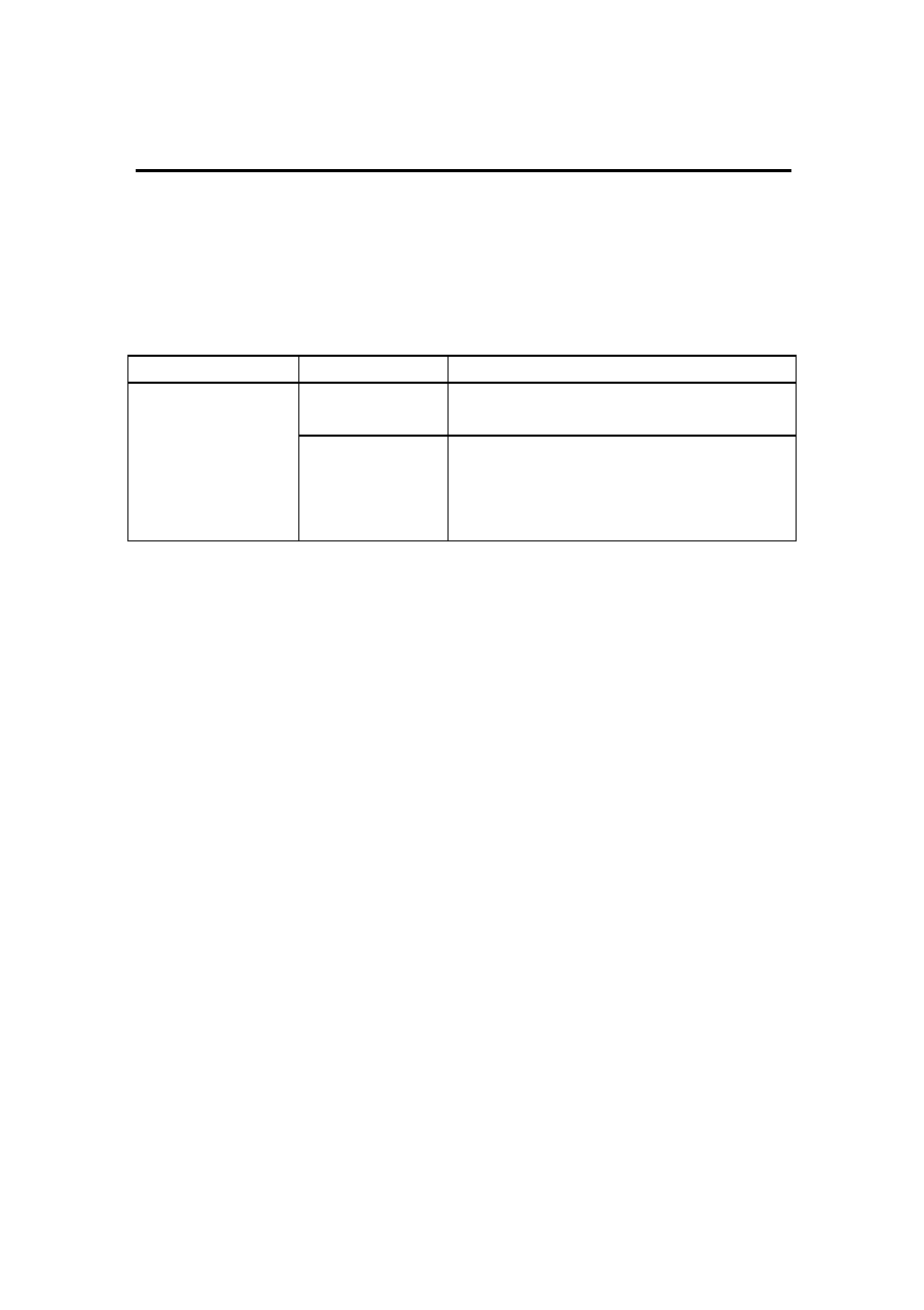
Load condition: Start pulse delay Time T
SD
on STH1 (STH2) output pin:
STH1(STH2)
Output
20pF
Load condition: Driver Output Delay Time T
DD
on output buffers:
25 k
Q to Q
A1
C80
25pF
Test point

CONFIDENTIAL
EUREKA
EK7601
- 20 -
Rev 1.0 Feb.21.2002
9. AC
CHARATERISTICS
WAVEFORM
Unless otherwise specified, the input level is defined to V
IH
= 0.7 V
DD
, V
IL
= 0.3 V
DD
CPH3
RESET
CPH2
CPH1
STH
input
STH
input
STH
input
STH
Output
STH
Output
INH
1
1
79
79
1
79
2
80
81
2
80
81
2
80
81
CPH1
1
2
3
4
5
1
2
CPH1'
x1 Mode
x3 Mode
78
79
80
81
234 235 236 237 238 239 240 241 242 243
243
244
244
High-Z
T
DD
T
C12
T
CWH
T
CWH
T
CWL
T
CWL
T
SD
T
SD
T
WR
T
IWL
T
IWH
T
RST-INH
T
INH-STH
T
SD
T
SD
T
CP
T
CP
T
C23
T
SS
T
SS
T
SS
T
SS
T
SH
T
SH
T
R
T
R
T
F
T
F
Target voltage
20mV
+
Q to Q
A1
C80
245
Table 9.1:
AC characteristics waveform
CONFIDENTIAL
EUREKA
EK7601
- 21 -
Rev 1.0 Feb.21.2002
10. RECOMMANDED SOLDERING CONDITIONS
The following conditions must be met for soldering conditions of the EK7601.
Please consult with our sales offices in case other soldering process is used, or in case the
soldering is done under different conditions.
EK7601: COF (TAB Package)
Mounting Condition
Mounting Method
Condition
Soldering
Heating tool 300 to 350∞C: heating for 2 to 3
Seconds: pressure 100g(per solder)
Thermocompression
ACF (Anisotropic
Conductive Film)
Temporary bonding 70 to 100∞C: pressure 3 to
8 kg/cm
2
: time 3 to 5 seconds.
Real bonding 165 to 180∞C: pressure 25 to 45
Kg/cm
2
: time 30 to 40 seconds.
11. LIFE SUPPORT APPLICATIONS
These products are not designed for use in life support appliances, devices, or systems where
malfunction of these products can reasonably be expected to result in personal injury. Eureka
customers using or selling these products for use in such applications do so at their own risk and
agree to fully indemnify Eureka for any damages resulting from such improper use or sale.