UF4001
THRU
UF4007
1.0 AMP HIGH EFFICIENCY RECTIFIERS
MAXIMUM RATINGS AND ELECTRICAL CHARACTERISTICS
Rating 25 C ambient temperature uniess otherwies specified.
Single phase half wave, 60Hz, resistive or inductive load.
For capacitive load, derate current by 20%.
TYPE NUMBER
Maximum Recurrent Peak Reverse Voltage
Maximum RMS Voltage
Maximum DC Blocking Voltage
Maximum Average Forward Rectified Current
.375"(9.5mm) Lead Length at Ta=50 C
FEATURES
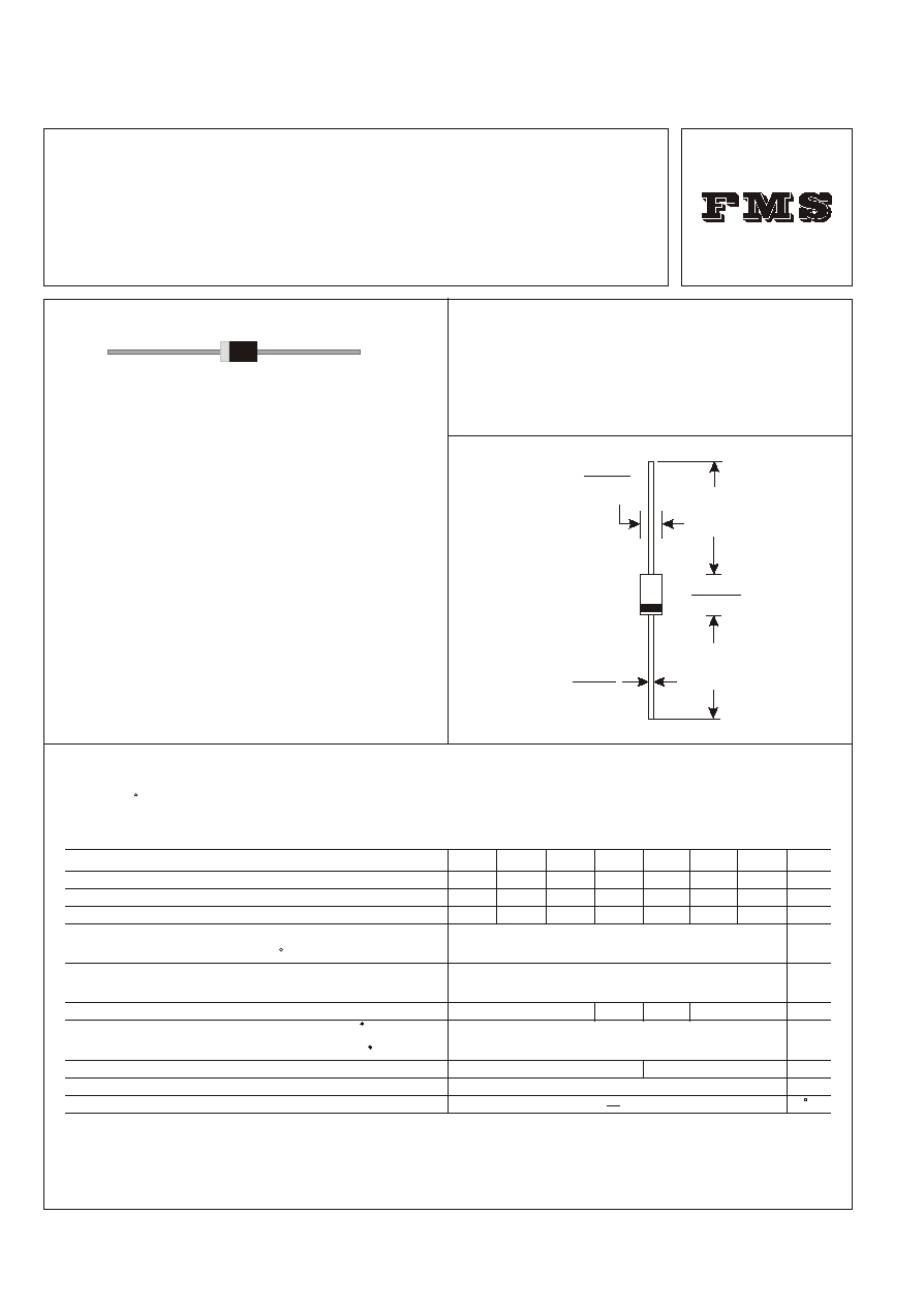
MECHANICAL DATA
Peak Forward Surge Current, 8.3 ms single half sine-wave
superimposed on rated load (JEDEC method)
Maximum Instantaneous Forward Voltage at 1.0A
Maximum DC Reverse Current Ta=25 C
at Rated DC Blocking Voltage Ta=100 C
Maximum Reverse Recovery Time (Note 1)
Typical Junction Capacitance (Note 2)
1.0
1.0
1.3
1.70
30
5.0
150
50 70
-65 +150
V
NOTES:
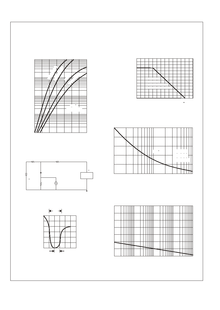
1. Reverse Recovery Time test condition: IF=0.5A, IR=1.0A, IRR=0.25A
2. Measured at 1MHz and applied reverse voltage of 4.0V D.C.
* Low forward voltage drop
* High current capability
* High reliability
* High surge current capability
* Case: Molded plastic
* Epoxy: UL 94V-0 rate flame retardant
* Lead: Axial leads, solderable per MIL-STD-202,
method 208 guranteed
* Polarity: Color band denotes cathode end
* Mounting position: Any
Weight: 0.34 grams
*
VOLTAGE RANGE
50 to 1000 Volts
CURRENT
1.0 Ampere
UF4001 UF4002 UF4003 UF4004 UF4005 UF4006 UF4007
UNITS
50 100 200 400 600 800 1000
50 100 200 400 600 800 1000
35 70 140 280 420 560 700
V
V
* High speed switching
DO-41
Dimensions in inches and (millimeters)
1.0(25.4)
MIN.
1.0(25.4)
MIN.
.205(5.2)
.166(4.2)
.034(.9)
.028(.7)
DIA.
.107(2.7)
.080(2.0)
DIA.
Operating and Storage Temperature Range T
J
, T
STG
A
A
V
mA
mA
nS
pF
C
1.5
15
.4
.6
.8
1.0
1.2
1.4
.001
.01
.1
1.0
10
RATING AND CHARACTERISTIC CURVES (UF4001 THRU UF4007)
FIG.1-TYPICAL FORWARD
CHARACTERISTICS
FIG.5-TYPICAL JUNCTION CAPACITANCE
I
N
S
T
A
N
T
A
N
E
O
U
S
F
O
R
W
A
R
D
C
U
R
R
E
N
T
,
(
A
)
FORWARD VOLTAGE,(V)
Pulse Width 300us
1% Duty Cycle
(+)
(+)
25Vdc
(approx.)
( )
( )
PULSE
GENERATOR
(NOTE 2)
OSCILLISCOPE
(NOTE 1)
1
NON-
INDUCTIVE
W
NOTES: 1. Rise Time= 7ns max., Input Impedance= 1 megohm.22pF.
2. Rise Time= 10ns max., Source Impedance= 50 ohms.
+0.5A
0
-0.25A
-1.0A
|
|
|
|
|
|
|
|
1cm
SET TIME BASE FOR
50 / 10ns / cm
trr
D.U.T.
FIG.3- TEST CIRCUIT DIAGRAM AND REVERSE
RECOVERY TIME CHARACTERISTICS
10
NONINDUCTIVE
50
NONINDUCTIVE
W
W
Tj=25 C
FIG.2-TYPICAL FORWARD CURRENT
A
V
E
R
A
G
E
F
O
R
W
A
R
D
C
U
R
R
E
N
T
,
(
A
)
0.2
0.4
0.6
0.8
1.0
1.2
Single Phase
Half Wave 60Hz
Resistive Or Inductive Load
0.375"(9.5mm) Lead Length
DERATING CURVE
AMBIENT TEMPERATURE ( C)
1.6 1.8
U
F4
00
5
U
F
4
0
0
4
U
F
4
0
0
1
~
U
F
4
0
0
3
REVERSE VOLTAGE,(V)
J
U
N
C
T
I
O
N
C
A
P
A
C
I
T
A
N
C
E
,
(
p
F
)
175
120
100
80
60
40
20
0
.01 .05 .1 .5 1 5 10 50 100
0
25
50 75 100 125 150 175
0
FIG.4-MAXIMUM NON-REPETITIVE FORWARD
SURGE CURRENT
6
0
12
18
24
30
NUMBER OF CYCLES AT 60Hz
1
10
5
50
100
Tj=25 C
8.3ms Single Half
Sine Wave
JEDEC method
P
E
A
K
F
O
R
W
A
R
D
S
U
R
G
E
C
U
R
R
E
N
T
,
(
A
)
UF
40
06
~U
F4
00
7