48
FOXElectronics
5570 Enterprise Parkway Fort Myers, Florida 33905 USA +001(239)693-0099
FAX +001(239)693-1554
http://www.foxonline.com
© 2003 FOX ELECTRONICS
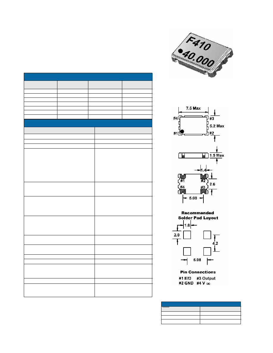
All dimensions are in millimeters.
FEATURES
∑ 3.3V Operation
∑ HCMOS Output
∑ Standby Function
∑ Tape and Reel
(2,000 pcs. STD)
∑ Pb Free
3.3V HCMOS SMD OSCILLATOR WITH STANDBY
F4100 SERIES
See
page 60
for tape and reel specifications.
OPTIONS
∑ 1.05mm Height Max
1
Inclusive of 25∫C tolerance, operating temperature range, input voltage change, load change, aging,
shock, and vibration.
2
An internal pullup resistor from pin 1 to pin 4 allows active output if pin 1 is left open.
See
page 30
for mechanical specifications, test circuits, and output waveform.
Note: A 0.01µF bypass capacitor should be placed between VDD (Pin 4) and GND (Pin 2) to
minimize power supply line noise.
All specifications subject to change without notice. Rev. 07/8/03
OUTPUT (Pin 3)
ACTIVE
ACTIVE
High Z
∑ ENABLE / DISABLE FUNCTION
INH (Pin 1)
OPEN
2
'1' Level V
IH
70% V
DD
'0' Level V
IL
30% V
DD
Frequency
Stability
1
±100PPM
±100PPM
±50PPM
±50PPM
±25PPM
±25PPM
±20PPM
∑ MODEL NUMBER SELECTION
Operating
Temperature (∫C)
-10 ~ +70
-40 ~ +85
-10 ~ +70
-40 ~ +85
-10 ~ +70
-40 ~ +85
-10 ~ +70
Frequency
Range (MHz)
0.012 ~ 170.000
0.012 ~ 170.000
0.012 ~ 170.000
0.012 ~ 170.000
0.012 ~ 132.000
0.012 ~ 100.000
0.012 ~ 132.000
F4100
F4100R
F4105
F4105R
F4106
F4106R
F4108
Model Number
0.012 ~ 170.000 MHz
-55∫C ~ +125∫C
3.3V ± 10%
3mA
6mA
15mA
20mA
25mA
40mA
45% ~ 55%
40% ~ 60%
6nS
4nS
3nS
6nS
4nS
3nS
10% V
DD
90% V
DD
Min
2mA Min
-2mA Min
15pF
10µA
5mS
10mS
150nS
5mS
10mS
PARAMETERS
Frequency Range (F
O
)
Storage Temperature Range (T
STG
)
Supply Voltage
(V
DD
)
Input Current
(I
DD
)
0.012 ~ 0.040 MHz
0.040+ ~ 1.500 MHz
1.500+ ~ 32.000 MHz
32.000+ ~ 50.000 MHz
50.000+ ~ 67.000 MHz
67.000+ ~ 170.000 MHz
Output Symmetry (50% V
DD
)
0.012 ~ 50.000 MHz
50.000+ ~ 170.000 MHz
Rise Time (10% ~ 90% V
DD
) (T
R
)
0.012 ~ 80.000 MHz
80.000+ ~ 125.000 MHz
125.000+ ~ 170.000 MHz
Fall Time (90% ~ 10% V
DD
) (T
F
)
0.012 ~ 80.000 MHz
80.000+ ~ 125.000 MHz
125.000+ ~ 170.000 MHz
Output Voltage
(V
OL
)
(V
OH
)
Output Current
(I
OL
)
(I
OH
)
Output Load
(HCMOS)
Standby Current
(V
IL
0.99V)
Start-up Time
(T
S
)
0.012 ~ 32.000 MHz
32.000+ ~ 170.000 MHz
Output Disable Time
2
Output Enable Time
2
0.012 ~ 32.000 MHz
32.000+ ~ 170.000 MHz
∑ ELECTRICAL CHARACTERISTICS
MAX
(unless otherwise noted)

49
© 2003 FOX ELECTRONICS
FOXElectronics
5570 Enterprise Parkway Fort Myers, Florida 33905 USA +001(239)693-0099
FAX +001(239)693-1554
http://www.foxonline.com
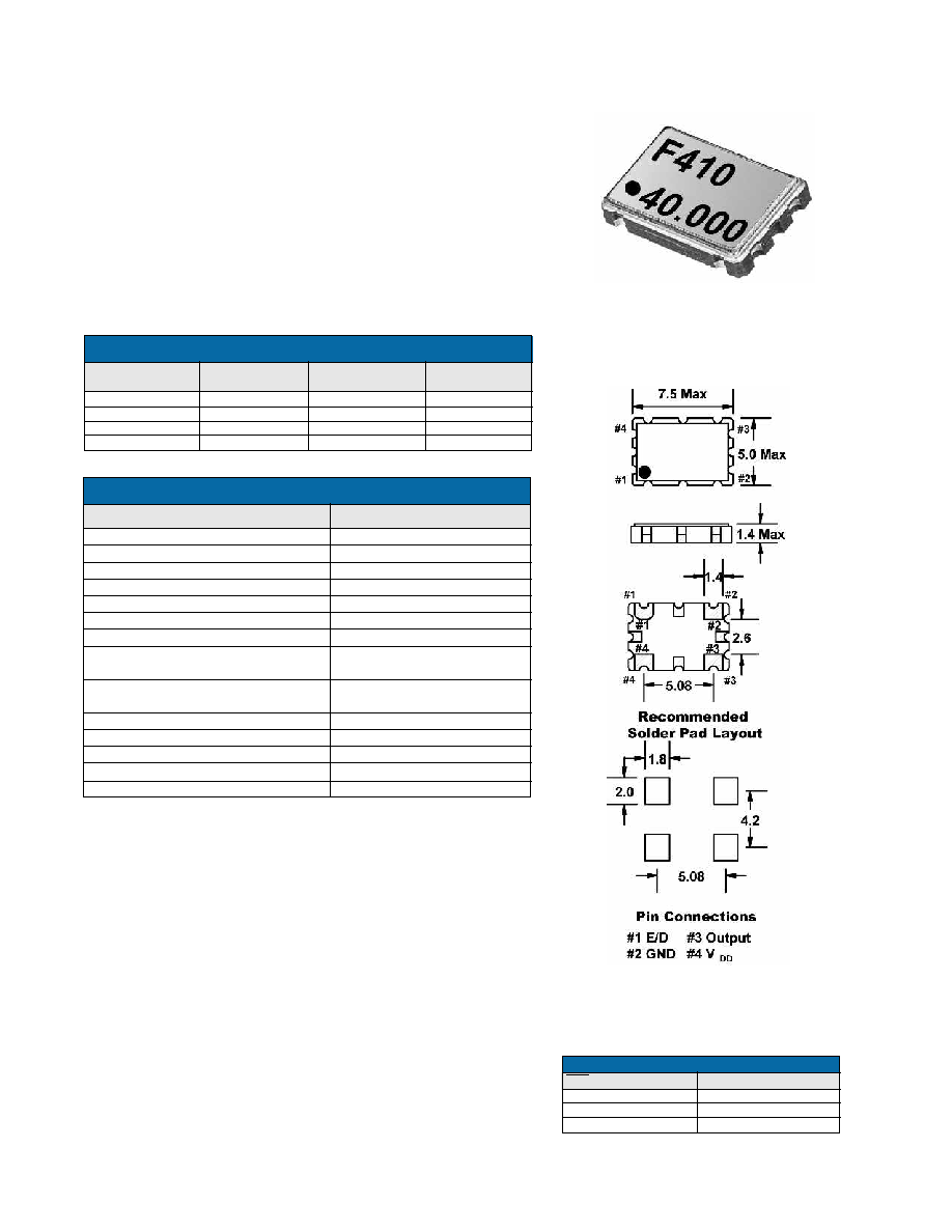
All dimensions are in millimeters.
FEATURES
∑ Tight Stability
∑ 3.3V Operation
∑ HCMOS Output
∑ Standby Function
∑ Tape and Reel
(2,000 pcs. STD)
∑ Pb Free
3.3V TIGHT STABILITY HCMOS SMD OSCILLATOR WITH STANDBY
F4100 SERIES
Frequency
Stability
1
±20PPM
±15PPM
±15PPM
±10PPM
∑ MODEL NUMBER SELECTION
Operating
Temperature (∫C)
-40 ~ +85
-10 ~ +70
-40 ~ +85
-10 ~ +70
Frequency
Range (MHz)
1.800 ~ 50.000
1.800 ~ 50.000
1.800 ~ 50.000
1.800 ~ 50.000
F4108R
F4107
F4107R
F4109
Model Number
See
page 60
for tape and reel specifications.
1
Inclusive of 25∫C tolerance, operating temperature range, input voltage change, load change, aging,
shock, and vibration.
2
An internal pullup resistor from pin 1 to pin 4 allows active output if pin 1 is left open.
See
page 30
for mechanical specifications, test circuits, and output waveform.
Note: A 0.01µF bypass capacitor should be placed between VDD (Pin 4) and GND (Pin 2) to
minimize power supply line noise.
All specifications subject to change without notice. Rev. 02/10/03
1.800 ~ 50.000 MHz
-55∫C ~ +125∫C
3.3V ± 5%
22 mA
45% ~ 55%
5nS
5nS
10% V
DD
90% V
DD
Min
8mA Min
4mA Min
15pF
50µA
5mS
150nS
5mS
PARAMETERS
Frequency Range (F
O
)
Storage Temperature Range (T
STG
)
Supply Voltage
(V
DD
)
Input Current
(I
DD
)
Output Symmetry (50% V
DD
)
Rise Time (10% ~ 90% V
DD
) (T
R
)
Fall Time (90% ~ 10% V
DD
) (T
F
)
Output Voltage
(V
OL
)
(V
OH
)
Output Current
(I
OL
)
(I
OH
)
Output Load
(HCMOS)
Standby Current
Start-up Time
(T
S
)
Output Disable Time
2
Output Enable Time
2
∑ ELECTRICAL CHARACTERISTICS
MAX
(unless otherwise noted)
OUTPUT (Pin 3)
ACTIVE
ACTIVE
High Z
∑ ENABLE / DISABLE FUNCTION
INH (Pin 1)
OPEN
2
'1' Level V
IH
70% V
DD
'0' Level V
IL
30% V
DD

