MW4IC001NR4 MW4IC001MR4
1
RF Device Data
Freescale Semiconductor
RF LDMOS Wideband Integrated
Power Amplifiers
The MW4IC001 wideband integrated circuit is designed for use as a distortion
signature device in analog predistortion systems. It uses Freescale's newest
High Voltage (26 to 28 Volts) LDMOS IC technology. Its wideband On Chip
design makes it usable from 800 MHz to 2170 MHz. The linearity performances
cover all modulations for cellular applications: GSM EDGE, TDMA, CDMA and
W-CDMA.
∑ Typical CW Performance at 2170 MHz, 28 Volts, I
DQ
= 12 mA
Output Power -- 900 mW PEP
Power Gain -- 13 dB
Efficiency -- 38%
∑ High Gain, High Efficiency and High Linearity
∑ Designed for Maximum Gain and Insertion Phase Flatness
∑ Excellent Thermal Stability
∑ Characterized with Series Equivalent Large-Signal Impedance Parameters
∑ N Suffix Indicates Lead-Free Terminations
∑ In Tape and Reel. R4 Suffix = 100 Units per 12 mm, 7 inch Reel.
Table 1. Maximum Ratings
Rating
Symbol
Value
Unit
Drain-Source Voltage
V
DSS
- 0.5, +65
Vdc
Gate-Source Voltage
V
GS
- 0.5, +15
Vdc
Total Device Dissipation @ T
C
= 25∞C
Derate above 25∞C
P
D
4.58
0.037
W
W/∞C
Storage Temperature Range
T
stg
- 65 to +150
∞C
Operating Junction Temperature
T
J
150
∞C
Table 2. Thermal Characteristics
Characteristic
Symbol
Value
Unit
Thermal Resistance, Junction to Case @ 85∞C
R
JC
27.3
∞C/W
Table 3. ESD Protection Characteristics
Test Conditions
Class
Human Body Model
0 (Minimum)
Machine Model
M1 (Minimum)
Charge Device Model
C2 (Minimum)
Table 4. Moisture Sensitivity Level
Test Methodology
Rating
Package Peak Temperature
Unit
Per JESD 22-A113, IPC/JEDEC J-STD-020
3
260
∞C
NOTE - CAUTION - MOS devices are susceptible to damage from electrostatic charge. Reasonable precautions in handling and
packaging MOS devices should be observed.
MW4IC001MR4
Rev. 3, 1/2005
Freescale Semiconductor
Technical Data
800-2170 MHz, 900 mW, 28 V
W-CDMA
RF LDMOS WIDEBAND
INTEGRATED POWER AMPLIFIERS
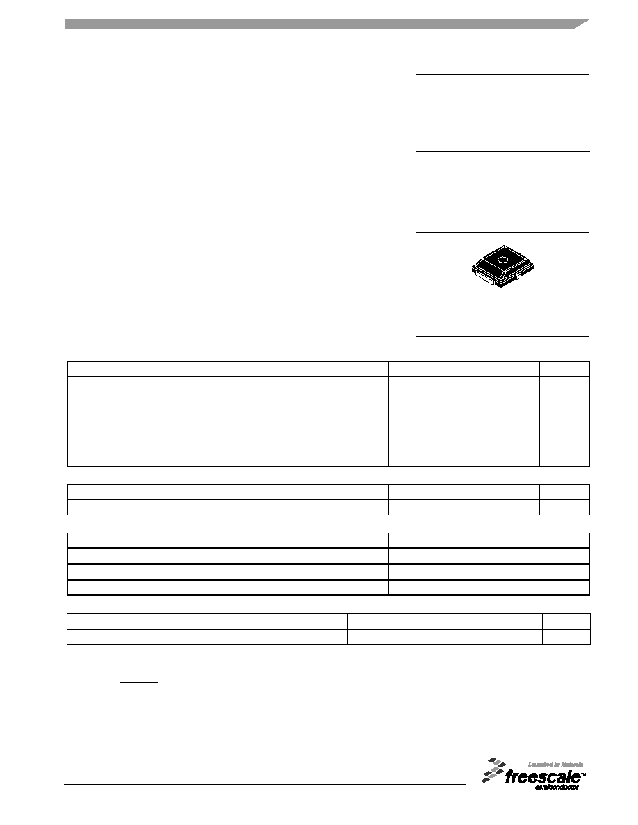
CASE 466-03, STYLE 1
PLD-1.5
PLASTIC
MW4IC001NR4
MW4IC001MR4
Freescale Semiconductor, Inc., 2005. All rights reserved.
2
RF Device Data
Freescale Semiconductor
MW4IC001NR4 MW4IC001MR4
Table 5. Electrical Characteristics
(T
C
= 25∞C unless otherwise noted)
Characteristic
Symbol
Min
Typ
Max
Unit
Off Characteristics
Zero Gate Voltage Drain Current
(V
DS
= 65 Vdc, V
GS
= 0 Vdc)
I
DSS
--
--
10
µAdc
Zero Gate Voltage Drain Current
(V
DS
= 28 Vdc, V
GS
= 0 Vdc)
I
DSS
--
--
10
µAdc
Gate-Source Leakage Current
(V
GS
= 5 Vdc, V
DS
= 0 Vdc)
I
GSS
--
--
1
µAdc
On Characteristics
Gate Threshold Voltage
(V
DS
= 10 V, I
D
= 50 µA)
V
GS(th)
2
3
5
Vdc
Gate Quiescent Voltage
(V
DS
= 28 V, I
D
= 10 mA)
V
GS(Q)
2
3.7
5
Vdc
Drain-Source On-Voltage
(V
GS
= 10 V, I
D
= 0.05 A)
V
DS(on)
--
0.48
0.9
Vdc
Forward Transconductance
(V
DS
= 10 V, I
D
= 0.1 A)
g
fs
--
0.05
--
S
Dynamic Characteristics
Output Capacitance
(V
DS
= 28
Vdc ± 30 mV(rms)ac @ 1 MHz, V
GS
= 0 Vdc)
C
oss
--
45
--
pF
Reverse Transfer Capacitance
(V
DS
= 28
Vdc ± 30 mV(rms)ac @ 1 MHz, V
GS
= 0 Vdc)
C
rss
--
0.62
--
pF
Functional Tests (In Freescale Test Fixture, 50 ohm system)
Two-Tone Common Source Amplifier Power Gain
(V
DD
= 28 Vdc, P
out
= 0.9 W PEP, I
DQ
= 12 mA,
f = 2170 MHz, Tone Spacing = 100 kHz)
G
ps
--
13
--
dB
Two-Tone Drain Efficiency
(V
DD
= 28 Vdc, P
out
= 0.9 W PEP, I
DQ
= 12 mA,
f = 2170 MHz, Tone Spacing = 100 kHz)
D
--
29
--
%
Third Order Intermodulation Distortion
(V
DD
= 28 Vdc, P
out
= 0.9 W PEP, I
DQ
= 12 mA,
f = 2170 MHz, Tone Spacing = 100 kHz)
IMD
--
- 28
--
dBc
Input Return Loss
(V
DD
= 28 Vdc, P
out
= 0.9 W PEP, I
DQ
= 12 mA,
f = 2170 MHz, Tone Spacing = 100 kHz)
IRL
--
-18
--
dB
Output Power, 1 dB Compression Point, CW
(V
DD
= 28 Vdc, I
DQ
= 12 mA, f = 2170 MHz)
P1dB
--
0.85
--
W
Common-Source Amplifier Power Gain
(V
DD
= 28 Vdc, P
out
= 0.9 W CW, I
DQ
= 12 mA, f = 2170 MHz)
G
ps
12
13
--
dB
Drain Efficiency
(V
DD
= 28 Vdc, P
out
= 0.9 W CW, I
DQ
= 12 mA, f = 2170 MHz)
D
35
38
--
%
Input Return Loss
(V
DD
= 28 Vdc, P
out
= 0.9 W CW, I
DQ
= 12 mA, f = 2170 MHz)
IRL
-10
-16
--
dB
MW4IC001NR4 MW4IC001MR4
3
RF Device Data
Freescale Semiconductor
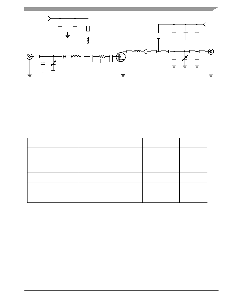
R2
Figure 1. MW4IC001NR4(MR4) 900 MHz Test Circuit Schematic
Z9
0.062 x 0.044 to 0.615 Taper
Z10
0.082 x 0.615 Microstrip
Z11
0.075 x 0.044 Microstrip
Z12
0.625 x 0.044 Microstrip
Z13
1.375 x 0.044 Microstrip
PCB
Rogers RO4350, 0.020,
r
= 3.5
Z1
1.331 x 0.044 Microstrip
Z2
0.126 x 0.076 Microstrip
Z3
0.065 x 0.175 Microstrip
Z4
0.065 x 0.195 Microstrip
Z5
0.680 x 0.145 Microstrip
Z6, Z7
1.915 x 0.055 Microstrip
Z8
0.120 x 0.141 Microstrip
RF
INPUT
Z1
V
GG
Z2
Z6
C4
Z3
RF
OUTPUT
C5
DUT
V
DD
Z9
Z11
Z13
Z7
Z5
C2
R1
C7
Z8
Z10
C8
+
Z12
C1
C9
L2
L1
C10
C3
C6
C11
C12
C13
Z4
Table 6. MW4IC001NR4(MR4) 900 MHz Test Circuit Component Designations and Values
Part
Description
Part Number
Manufacturer
C1, C6
0.1 µF, 100 V Chip Capacitors
C1210C104K5RACTR
Kemet
C2, C3, C5, C7
43 pF, 500 V Chip Capacitors
100B430JP500X
ATC
C4
12 pF, 500 V Chip Capacitor
100B120JP500X
ATC
C8
22 µF, 35 V Tantalum Chip Capacitor
T491X226K035AS
Kemet
C9
4.7 pF, 500 V Chip Capacitor
100B4R7CP500X
ATC
C10, C11
0.6-4.5 pF, 500 V Variable Capacitors
27271SL
Johanson
C12
2.7 pF, 500 V Chip Capacitor
100B2R7CP500X
ATC
C13
3.3 pF, 500 V Chip Capacitor
100B3R3CP500X
ATC
L1
5.6 nH Chip Inductor
0805 Series
AVX
L2
10 nH Chip Inductor
1008 Series
ATC
R1
100 W Chip Resistor
CRCW12061001F100
Dale
R2
20 W Chip Resistor
CRCW120620R0F100
Dale
4
RF Device Data
Freescale Semiconductor
MW4IC001NR4 MW4IC001MR4
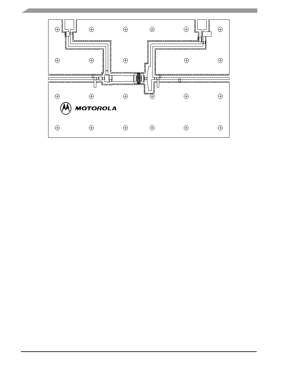
C8
Figure 2. MW4IC001NR4(MR4) 900 MHz Test Circuit Component Layout
VGG
VDD
900 MHz
MW4IC001MR4
C6
C1
C7
C2
R1
C10
C13
Rev 2
C3
C9
L1
C4
R2
L2
C12
C11
C5
Freescale has begun the transition of marking Printed Circuit Boards (PCBs) with the Freescale Semiconductor
signature/logo. PCBs may have either Motorola or Freescale markings during the transition period. These changes will have
no impact on form, fit or function of the current product.
MW4IC001NR4 MW4IC001MR4
5
RF Device Data
Freescale Semiconductor
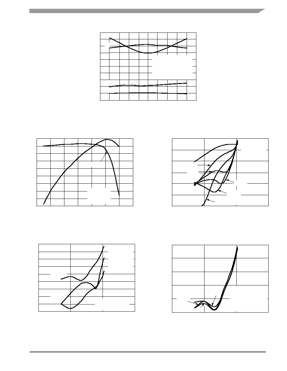
TYPICAL CHARACTERISTICS - 900 MHz
905
50
-35
-15
f1, FREQUENCY (MHz)
Figure 3. Two-Tone Performance versus
Frequency
INTERMODULA
TION DIST
ORTION
(dBc)
IMD,
INPUT
RETURN LOSS (dB)
IRL,
V
DS
= 28 Vdc
P
out
= 0.9 W (PEP)
I
DQ
= 14 mA
Two -Tone Measurement
100 kHz Tone Spacing
D
IRL
G
ps
IM3
-17
-19
-21
-23
-25
-27
-29
-31
-33
46
42
38
34
30
26
22
18
14
10
900
895
890
885
880
875
870
865
860
855
60
55
50
45
40
35
30
25
20
15
15
0
P1dB
P
out
, OUTPUT POWER (WATTS)
Figure 4. CW Performance versus Output
Power
G
ps
, POWER GAIN (dB)
V
DS
= 28 Vdc
I
DQ
= 14 mA
f = 880 MHz
G
ps
14
13
12
11
10
9
8
7
6
0.2
0.4
0.6
0.8
1.0
1.2
1.4
10
-25
-30
-35
-40
-45
-50
-55
1
0.1
0.01
I
DQ
= 8 mA
12 mA
P
out
, OUTPUT POWER (WATTS) PEP
Figure 5. Intermodulation Distortion versus
Output Power
INTERMODULA
TION DIST
ORTION
(dBc)
IMD,
10 mA
16 mA
14 mA
18 mA
10
-25
3rd Order
P
out
, OUTPUT POWER (WATTS) PEP
Figure 6. Intermodulation Distortion Products
versus Output Power
INTERMODULA
TION DIST
ORTION
(dBc)
IMD,
V
DS
= 28 Vdc
I
DQ
= 14 mA
f1 = 880 MHz
f2 = 880.1 MHz
5th Order
7th Order
-30
-35
-40
-45
-50
-55
-60
-65
-70
1
0.1
0.01
10
-25
10 MHz
P
out
, OUTPUT POWER (WATTS) PEP
Figure 7. Third Order Intermodulation
Distortion versus Output Power
INTERMODULA
TION DIST
ORTION
(dBc)
IMD,
V
DS
= 28 Vdc
I
DQ
= 14 mA
f1 = 880 MHz,
f2 = f1 + Tone Spacing
Two -Tone Measurement
-30
-35
-40
-45
-50
1
0.1
0.01
1 MHz
Tone
Spacing = 100 kHz
Two -Tone Measurement
100 kHz Tone Spacing
V
DS
= 28 Vdc
f1 = 880 MHz
f2 = 880.1 MHz
Two -Tone Measurement
100 kHz Tone Spacing
D
D
, DRAIN EFFICIENCY (%), G
ps
, POWER GAIN (dB)
D
, DRAIN EFFICIENCY (%)