
Order this document
by AN1746/D
AN1746
Migrating from the MC68HC705K1 to the MC68HC705KJ1
By Mark Glenewinkel
Field Applications Engineering
Consumer Systems Group
Austin, Texas
Introduction
Freescale provides two different parts to migrate your current
MC68HC705K1 (K1) application easily. Depending on your design,
system enhancements, and cost, the MC68HC705KJ1 (KJ1) and the
MC68HC805K3 (K3) provide two different migration paths.
The major differences between the KJ1 and the K3 are:
� Price
� Pinout compatibility
The KJ1 is not pin for pin the same as the K1, but it is roughly 70% the
cost of the K1. Although the K3 is pin for pin the same as the K1, it is
roughly 90% the cost of the K1.
This application note illustrates the differences between the K1 and the
KJ1. Using the KJ1's additional features can further enhance your
system design. Consult the K1 and KJ1 databooks for detailed design
reference. See
References/Additional Reading
in this application
note.
F
r
e
e
s
c
a
l
e
S
e
m
i
c
o
n
d
u
c
t
o
r
,
I
Freescale Semiconductor, Inc.
For More Information On This Product,
Go to: www.freescale.com
n
c
.
.
.
Freescale Semiconductor
� Freescale Semiconductor, Inc., 2004. All rights reserved.

Application Note
AN1746
For information on migrating your design to the K3, consult the
application note titled
Migrating from the MC68HC705K1 to the
MC68HC805K3, Freescale document order number AN1747/D.
MC68HC705KJ1
Features
� 1240 bytes of user EPROM
� 64 bytes of low-power user RAM
� 4-MHz maximum internal bus frequency at 5 volts
� 15-stage multifunction timer
� COP watchdog timer
� 10 bidirectional input/output (I/O) pins, including:
� 10-mA sink capability on all I/O pins
� 5.5-mA source capability on six I/O pins
� Software programmable pulldowns on all I/O pins
� Keyboard scan with selectable interrupt on four I/O pins
� Selectable sensitivity on external interrupt; edge- and level-
sensitive or edge-sensitive only
� On-chip oscillator with options for:
� Crystal
� Ceramic resonator
� Resistor-capacitor (RC) oscillator (MC68HRC705KJ1) with or
without external resistor
� Low-speed (32 kHz) crystal (MC68HLC705KJ1)
� External clock
� External interrupt mask bit and acknowledge bit
� EPROM security bit
1
to aid in locking out access to programmable
EPROM array
� Selectable STOP conversion to HALT and option for fast restart
and power-on reset
� Internal steering diode and pullup device on RESET pin to V
DD
1. No security feature is absolutely secure. However, Motorola's strategy is to make reading or
copying the EPROM/OTPROM difficult for unauthorized users.
F
r
e
e
s
c
a
l
e
S
e
m
i
c
o
n
d
u
c
t
o
r
,
I
Freescale Semiconductor, Inc.
For More Information On This Product,
Go to: www.freescale.com
n
c
.
.
.
Application Note
Migrating to the MC68HC705KJ1
AN1746
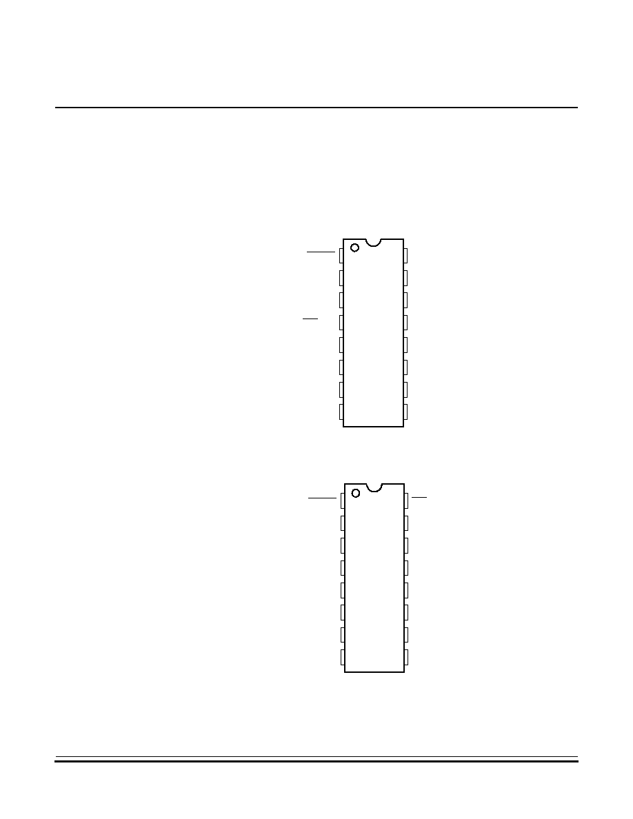
Migrating to the MC68HC705KJ1
Pinouts and
Package Types
The KJ1 has a different pinout from the K1, making layout changes
necessary. See
Figure 1
and
Figure 2
for pin descriptions.
Both parts are available in either plastic DIP or SOIC packages.
Figure 1. MC68HC705K1 Pinout
Figure 2. MC68HC705KJ1 Pinout
RESET
OSC1
OSC2
V
SS
V
DD
PA7
PA6
PA5
PA4
1
2
3
4
5
6
7
8
16
15
14
13
12
11
10
9
PB1/OSC3
PB0
IRQ/V
PP
PA0
PA1
PA2
PA3
IRQ/V
PP
PA0
PA1
PA2
PA3
PA4
PA5
PA6
1
2
3
4
5
6
7
8
16
15
14
13
12
11
10
9
OSC1
OSC2
PB3
PB2
V
DD
V
SS
PA7
RESET
F
r
e
e
s
c
a
l
e
S
e
m
i
c
o
n
d
u
c
t
o
r
,
I
Freescale Semiconductor, Inc.
For More Information On This Product,
Go to: www.freescale.com
n
c
.
.
.

Application Note
AN1746
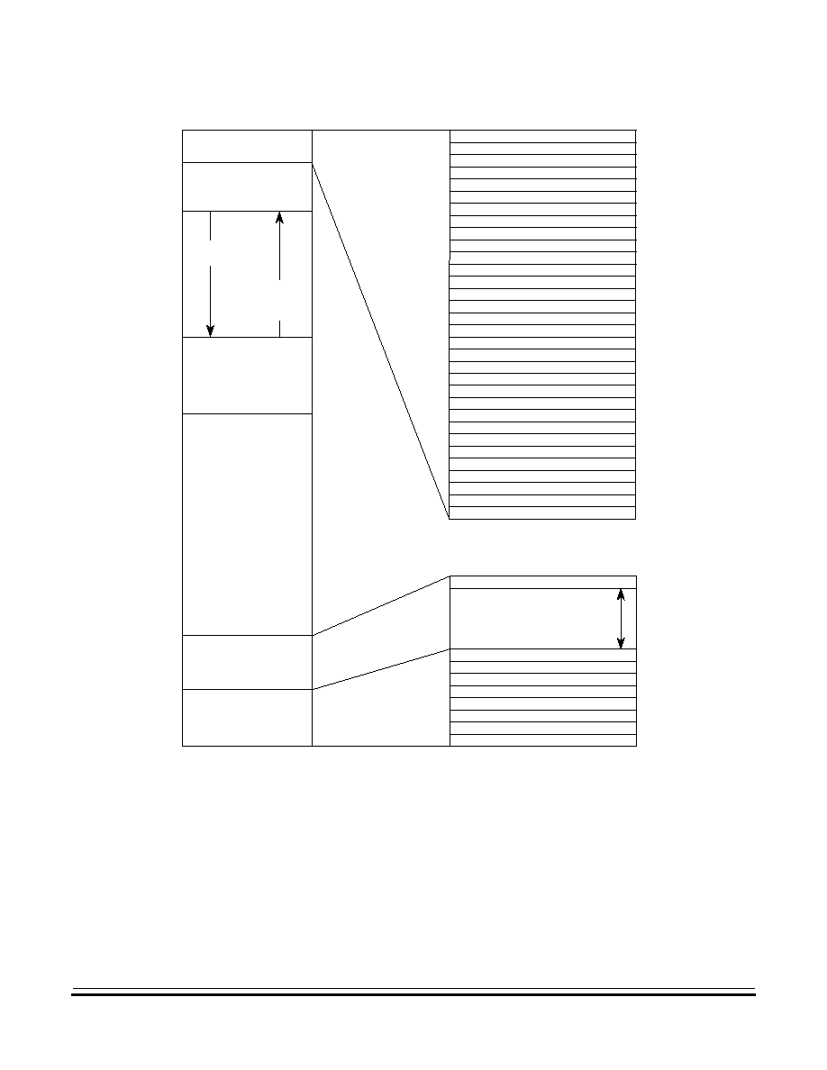
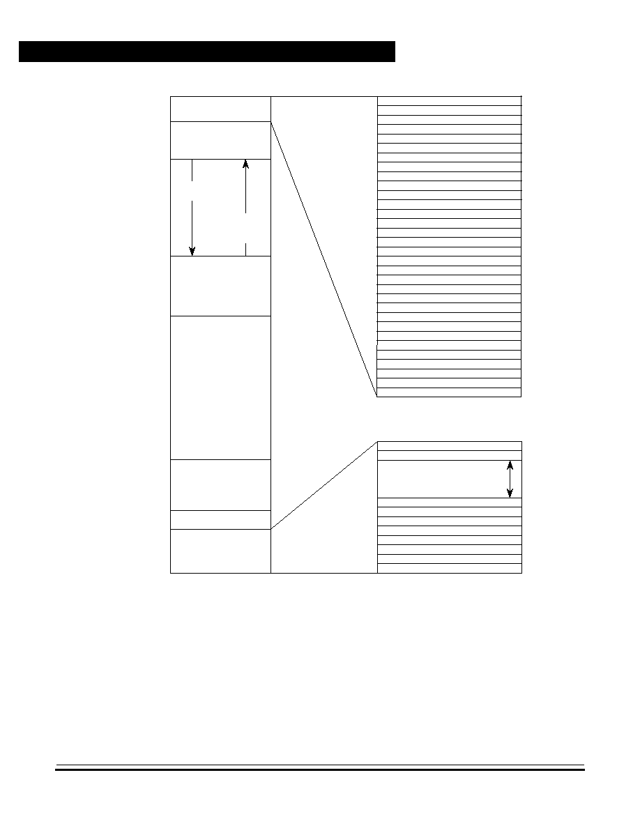
Block Diagrams
Throughout this application note, refer to the block diagrams for the K1
in
Figure 3
and KJ1 in
Figure 4
.
Figure 3. MC68HC705K1 Block Diagram
DATA DIRECTION REGISTER B
PORT B
PB1/OSC3
PB0
0 0 0
0 0 0
0 0
1 1
CPU CONTROL
ARITHMETIC/LOGIC
UNIT
ACCUMULATOR
INDEX REGISTER
STACK POINTER
0 0 0
PROGRAM COUNTER
0 0
M68HC05
MCU
RESET
CONDITION CODE REGISTER
1 1 1 H I
N C Z
DATA DIRECTION REGISTER A
PORT A
PA7*
PA6*
PA5*
PA4*
PA3**
PA2**
PA1**
PA0**
*8-mA-sink capability
**External interrupt capability
COP WATCHDOG
AND
INTERNAL
OSCILLATOR
DIVIDE
BY TWO
MULTIFUNCTION
ILLEGAL ADDRESS
DETECT
LOW-VOLTAGE
IRQ/V
PP
V
DD
V
SS
OSC1
OSC2
PERSONALITY EPROM/OTPROM-- 64 BITS
USER RAM -- 32 BYTES
RESET
MASK OPTION REGISTER (EPROM/OTPROM)
USER EPROM/OTPROM -- 504 BYTES
1
0
TIMER
CPU
CLOCK
TIMER
CLOCK
DETECT
F
r
e
e
s
c
a
l
e
S
e
m
i
c
o
n
d
u
c
t
o
r
,
I
Freescale Semiconductor, Inc.
For More Information On This Product,
Go to: www.freescale.com
n
c
.
.
.

Application Note
Migrating to the MC68HC705KJ1
AN1746
Figure 4. MC68HC705KJ1 Block Diagram
0 0 0 0 0 0 0 0 1 1
WATCHDOG AND
ILLEGAL ADDRESS
DETECT
STATIC RAM (SRAM) � 64 BYTES
ALU
CPU CONTROL
68HC05 CPU
ACCUMULATOR
INDEX REGISTER
STK PTR
PROGRAM COUNTER
CONDITION CODE
REGISTER
15-STAGE
MULTIFUNCTION
TIMER SYSTEM
DIVIDE
INTERNAL
OSCILLATOR
OSC1
OSC2
CPU REGISTERS
USER EPROM � 1240 BYTES
MASK OPTION REGISTER (EPROM)
10-mA sink capability on all I/O pins
DATA DIRECTION REGISTER A
DATA DIRECTION REGISTER B
PORT A
PORT B
PB3
(1)
PB2
(1)
PA7
PA6
PA5
PA4
PA3
(1) (2)
PA2
(1) (2)
PA1
(1) (2)
PA0
(1) (2)
RESET
IRQ/V
PP
1 1 1 H I N Z C
BY 2
NOTES:
1. 5.5-mA source capability
2. External interrupt capability
F
r
e
e
s
c
a
l
e
S
e
m
i
c
o
n
d
u
c
t
o
r
,
I
Freescale Semiconductor, Inc.
For More Information On This Product,
Go to: www.freescale.com
n
c
.
.
.

Application Note
AN1746
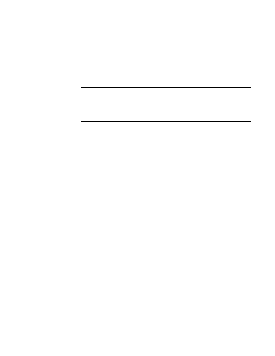
Memory Maps
and Registers
Figure 5
and
Figure 6
show the memory maps and registers of the K1
and KJ1. Modify your code to reflect these changes:
� The KJ1 has a total of 64 bytes of RAM. If you want to utilize this
additional memory of the KJ1, originate RAM memory to start at
$C0.
� The KJ1 has a total of 1232 bytes of EPROM for code space.
Originate EPROM memory to start at $300.
� Move the MOR register from location $17 on the K1 to location
$7F1 on the KJ1.
� Move the location of the COP register from location $3F0 on the
K1 to location $7F0 on the KJ1.
� Move the start of the interrupt vectors from location $3F8 on the
K1 to location $7F8 on the KJ1.
F
r
e
e
s
c
a
l
e
S
e
m
i
c
o
n
d
u
c
t
o
r
,
I
Freescale Semiconductor, Inc.
For More Information On This Product,
Go to: www.freescale.com
n
c
.
.
.
Application Note
Migrating to the MC68HC705KJ1
AN1746
Figure 5. MC68HC705K1 Memory and Register Map
Port A Data Register
Timer Interrupt Vector (MSB)
Timer Interrupt Vector (LSB)
External Interrupt Vector (MSB)
External IInterrupt Vector (LSB)
Software Interrupt Vector (MSB)
Software Interrupt Vector (LSB)
Reset Vector (MSB)
Reset Vector (LSB)
$000F
$000E
$0009
$0008
$0007
$0006
$0005
$0004
$0003
$0002
$0001
$0000
$03F8
$03F9
$03FA
$03FB
$03FC
$03FD
$03FE
$03FF
Port B Data Register
Port A Data Direction Register
Port B Data Direction Register
�
�
�
COP Register
$03F0
UNUSED
192 BYTES
$0000
$001F
$03FF
I/O REGISTERS
32 BYTES
USER VECTORS
EPROM
8 BYTES
TEST ROM AND
8 BYTES
$03F7
$01FF
UNUSED
256 BYTES
SRAM
32 BYTES
Unused
Unused
Unused
Unused
Timer Counter Register
Timer Status and Control Register
$000A
IRQ Status and Control Register
$0200
$00DF
$00E0
$0020
$00FF
$0100
$03F8
USER EPROM
496 BYTES
RESERVED
7 BYTES
$03EF
$03F0
32 BYTES
$0010
$0011
$0012
STACK
COP REGISTER
Unused
Unused
Unused
PEPROM Bit Select Register
$000C
$000B
$000D
PEPROM Status and Control Register
Pulldown Register A
Pulldown Register B
$001F
$001E
$0019
$0018
$0017
$0016
$0015
$0014
$0013
$001A
$001C
$001B
$001D
Unused
Unused
Unused
Unused
Unused
Mask Option Register
EPROM Programming Register
Unused
Unused
Unused
Unused
Unused
Unused
Test
SRAM
F
r
e
e
s
c
a
l
e
S
e
m
i
c
o
n
d
u
c
t
o
r
,
I
Freescale Semiconductor, Inc.
For More Information On This Product,
Go to: www.freescale.com
n
c
.
.
.
Application Note
AN1746
Figure 6. MC68HC705KJ1 Memory and Register Map
Port A Data Register
Timer Interrupt Vector (MSB)
Timer Interrupt Vector (LSB)
External Interrupt Vector (MSB)
External IInterrupt Vector (LSB)
Software Interrupt Vector (MSB)
Software Interrupt Vector (LSB)
Reset Vector (MSB)
Reset Vector (LSB)
$000F
$000E
$0009
$0008
$0007
$0006
$0005
$0004
$0003
$0002
$0001
$0000
$07F8
$07F9
$07FA
$07FB
$07FC
$07FD
$07FE
$07FF
Port B Data Register
Port A Data Direction Register
Port B Data Direction Register
�
�
�
COP Register
$07F0
UNUSED
160 BYTES
$0000
$001F
$07FF
I/O REGISTERS
32 BYTES
REGISTERS & VECTORS
(EPROM)
16 BYTES
TEST ROM
2 BYTES
$07EF
$02FF
UNUSED
512 BYTES
SRAM
64 BYTES
Unused
Unused
Unused
Unused
Timer Counter Register
Timer Status and Control Register
$000A
IRQ Status and Control Register
$0300
$00BF
$00C0
$0020
$00FF
$0100
$07F0
USER EPROM
1232 BYTES
RESERVED
6 BYTES
$07ED
$07EE
64 BYTES
$0010
$0011
$0012
Unused
Unused
Unused
$000C
$000B
$000D
Pulldown Register A
Pulldown Register B
$001F
$001E
$0019
$0018
$0017
$0016
$0015
$0014
$0013
$001A
$001C
$001B
$001D
Unused
Unused
Unused
Unused
Unused
EPROM Programming Register
Unused
Unused
Unused
Unused
Unused
Unused
Reserved
Unused
Unused
Unused
Mask Option Register
$07F1
$07CF
$07D0
UNUSED
30 BYTES
STACK
SRAM
F
r
e
e
s
c
a
l
e
S
e
m
i
c
o
n
d
u
c
t
o
r
,
I
Freescale Semiconductor, Inc.
For More Information On This Product,
Go to: www.freescale.com
n
c
.
.
.
Application Note
Migrating to the MC68HC705KJ1
AN1746
Ports
The KJ1 I/O pins have expanded high current capabilities that allow
them to source or sink current to a device. Depending on the current
requirements, these pins can be used to switch power to other parts of
the system, light LEDs, or switch opto-coupled triacs without external
transistors.
Table 1
shows the maximum ratings for the I/O pins.
Consult the KJ1 databook for high-side and low-side driver
characteristics and graphs.
Port A
No changes needed on port A.
Port B
The KJ1 has two bits of the port B register bonded out. These are bits 2
and 3. Change your code by mapping the K1's port B pins to the KJ1's
port B pins. This mapping also applies to the port B data direction
register and the port B pulldown register.
K1 PB0 maps to KJ1 PB2.
K1 PB1 maps to KJ1 PB3.
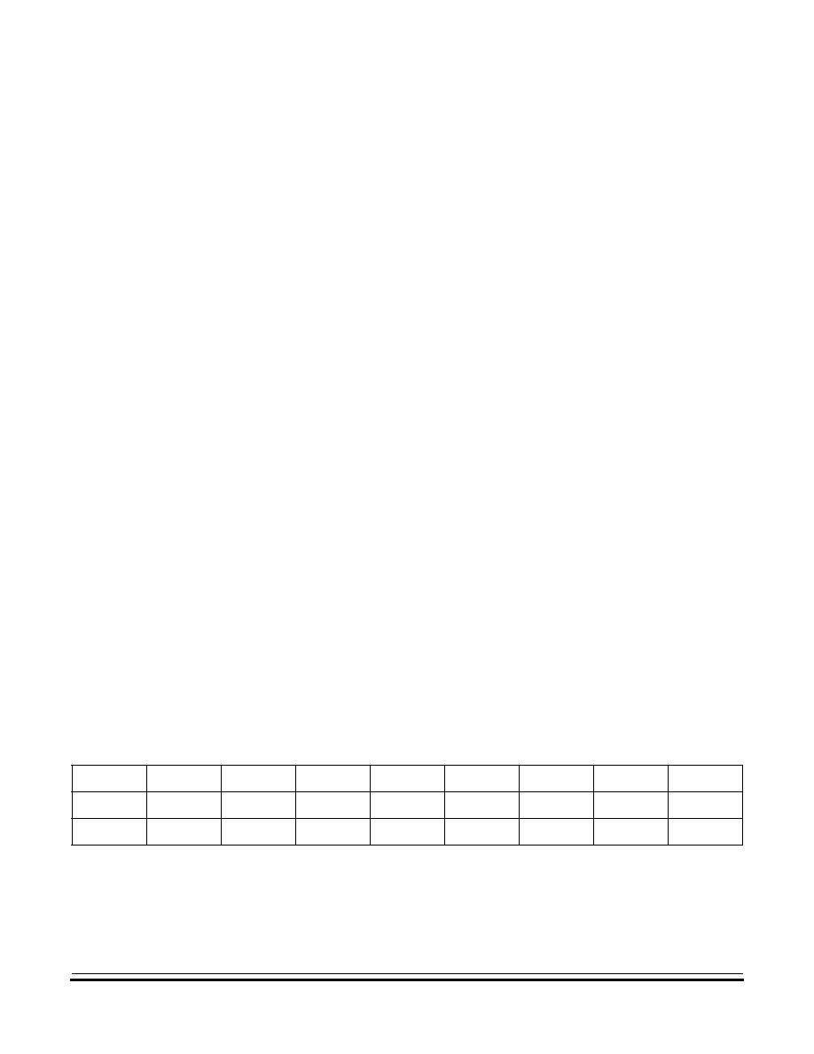
Table 1. KJ1 I/O Maximum Current Ratings
Characteristic
Symbol
Max
Unit
High source current
PA7�PA4 pins
PA3�PA0 pins
PB3�PB2 pins
I
OH
2.5
5.5
5.5
mA
High sink current
PA7�PA0 pins
PB3�PB2 pins
I
OL
10
10
mA
F
r
e
e
s
c
a
l
e
S
e
m
i
c
o
n
d
u
c
t
o
r
,
I
Freescale Semiconductor, Inc.
For More Information On This Product,
Go to: www.freescale.com
n
c
.
.
.
Application Note
AN1746
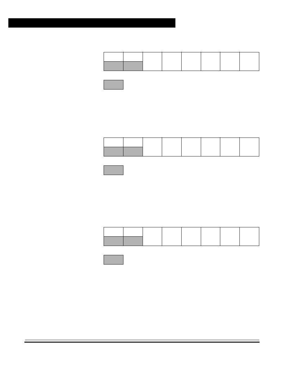
Figure 7. Port B Data Register (PORTB)
Figure 8. Port B Data Direction Register (DDRB)
Figure 9. Pulldown Register B (PDRB)
$0001
Bit 7
6
5
4
3
2
1
Bit 0
Read:
0
0
See
Note
See
Note
PB3
PB2
See
Note
See
Note
Write:
Reset:
Unaffected by reset
= Unimplemented
PB5, PB4, PB1, and PB0 should be configured as inputs at all times. These bits are avail-
able for read/write but are not available externally. Configuring them as inputs will en-
sure that the pulldown devices are enabled, thus properly terminating them.
$0005
Bit 7
6
5
4
3
2
1
Bit 0
Read:
0
0
See
Note
See
Note
DDRB3
DDRB2
See
Note
See
Note
Write:
Reset:
0
0
0
0
0
0
0
0
= Unimplemented
PB5, PB4, PB1, and PB0 should be configured as inputs at all times. These bits are avail-
able for read/write but are not available externally. Configuring them as inputs will en-
sure that the pulldown devices are enabled, thus properly terminating them.
$0011
Bit 7
6
5
4
3
2
1
Bit 0
Read:
0
0
See
Note
See
Note
PDIB3
PDIB2
See
Note
See
Note
Write:
Reset:
0
0
0
0
0
0
0
0
= Unimplemented
PB5, PB4, PB1, and PB0 should be configured as inputs at all times. These bits are avail-
able for read/write but are not available externally. Configuring them as inputs will en-
sure that the pulldown devices are enabled, thus properly terminating them.
F
r
e
e
s
c
a
l
e
S
e
m
i
c
o
n
d
u
c
t
o
r
,
I
Freescale Semiconductor, Inc.
For More Information On This Product,
Go to: www.freescale.com
n
c
.
.
.

Application Note
Migrating to the MC68HC705KJ1
AN1746
Clock
The KJ1 has different clock circuitry than the K1. The main difference is
the RC clock option. The available clocking options on the KJ1 are listed
in
Table 2
.
If you are using a crystal or ceramic resonator and want to use the
internal feedback resistor, the OSCRES bit in the mask option register
(MOR) must be set to 1. This enables the 2-M
feedback resistor. The
KJ1 has the option of using a 32-kHz crystal. Consult the KJ1 databook
about how to connect a 32-kHz crystal to the KJ1 properly.
The RC option on the KJ1 is quite different from the K1. The RC
oscillator has two options:
� For more accurate clocks, use an external resistor between the
OSC1 and OSC2 pins. Do not turn on the internal feedback
resistor. Make sure the OSCRES bit in the MOR is 0.
� For maximum cost reduction, the RC oscillator can utilize the
internal resistor and allow the chip to be driven with no external
components. This is also the least accurate way to clock the chip.
To use this option, make sure that the OSCRES bit in the MOR
is 1.
Like the K1, the KJ1 can be driven by an external clocking source also.
Table 2. KJ1 Clock Options
Clock Option
Comments
Part Number
Crystal oscillator
Internal feedback resistor
con gured in MOR
MC68HC705KJ1
Crystal oscillator (32 kHz)
Do not use internal
feedback resistor
MC68HLC705KJ1
Ceramic resonator
Internal feedback resistor
con gured in MOR
MC68HC705KJ1
RC oscillator
Uses either external or
internal resistor
MC68HRC705KJ1
External clock
Direct connection of clock
source
MC68HC705KJ1
F
r
e
e
s
c
a
l
e
S
e
m
i
c
o
n
d
u
c
t
o
r
,
I
Freescale Semiconductor, Inc.
For More Information On This Product,
Go to: www.freescale.com
n
c
.
.
.

Application Note
AN1746
For applications that demand more performance, the KJ1 maximum
internal clock frequency is 4 MHz. The K1 maximum internal clock
frequency is 2 MHz.
Reset and LVR
Circuitry
The reset function on the KJ1 has additional features:
� The RESET pin contains a steering diode to discharge any voltage
on the pin to V
DD
when the power is removed.
� The RESET pin contains an internal pullup resistor to V
DD
to allow
the RESET pin to be left unconnected for low-power applications.
� The KJ1 has all of the K1 reset sources except a low-voltage reset
(LVR). These are:
� Power-on reset
� Logic 0 on the RESET pin
� Computer operating properly (COP)
� Illegal address
The KJ1 does not have an internal LVR. If your K1 design used the LVR,
external LVR circuitry must be added to replace this function.
Interrupts
Like the K1, the KJ1 has the same interrupt sources and functionality.
These are:
� Software interrupt
� Logic 0 applied to the IRQ/V
PP
pin
� Logic 1 applied to one of the PA3�PA0 pins
� A timer overflow interrupt
� A real-time interrupt
The port A interrupt option on the K1 is programmed by writing to the
PIRQ bit (bit 2) of the MOR at location $17. On the KJ1, write to the PIRQ
bit (bit 2) of the MOR at location $7F1.
The external interrupt sensitivity on the K1 is programmed by writing to
the LEVEL bit (bit 1) of the MOR at location $17. On the KJ1, write to the
LEVEL bit (bit 1) of the MOR at location $7F1.
F
r
e
e
s
c
a
l
e
S
e
m
i
c
o
n
d
u
c
t
o
r
,
I
Freescale Semiconductor, Inc.
For More Information On This Product,
Go to: www.freescale.com
n
c
.
.
.
Application Note
Migrating to the MC68HC705KJ1
AN1746
Timer
The timer on the KJ1 is identical to the K1. No changes are needed in
software or hardware.
COP
The COP on the K1 is enabled by programming the COPEN bit (bit 0) of
the MOR at location $17 to a 1. On the KJ1, program the COPEN bit (bit
0) of the MOR at location $7F1 to a 1.
The K1 COP timer is cleared by writing a 0 to bit 0 of the COPR
(computer operating properly register) at location $3F0. On the KJ1,
clear the COP by writing a 0 to bit 0 of the COPR located at $7F0.
Just like the K1, the KJ1 COP timeout is set by the RT1 and RT0 bits of
the timer status and control register. No code changes are needed.
Personality EPROM
The K1 provides the user with 64 bits of personality EPROM. The KJ1
does not have a personality EPROM array. Consequently, the
personality EPROM bit select register and the personality EPROM
status and control register are not found on the KJ1.
To provide this functionality within the KJ1, utilize some of the extra
EPROM on the KJ1 to create eight bytes or 64 bits of personality
EPROM. This EPROM memory cannot be programmed by the user's
code. It can be programmed only at the time the entire EPROM array is
being programmed for production.
MOR
The KJ1 gives the designer additional options in the MOR.
Table 3
compares the two MOR registers.
Table 3. MOR Comparison
Part
Bit 7
Bit 6
Bit 5
Bit 4
Bit 3
Bit 2
Bit 1
Bit 0
K1
SWPDI
PIN3
RC
SWAIT
LVRE
PIRQ
LEVEL
COPEN
KJ1
SOSCD
EPMSEC
OSCRES
SWAIT
SWPDI
PIRQ
LEVEL
COPEN
F
r
e
e
s
c
a
l
e
S
e
m
i
c
o
n
d
u
c
t
o
r
,
I
Freescale Semiconductor, Inc.
For More Information On This Product,
Go to: www.freescale.com
n
c
.
.
.

Application Note
AN1746
SWPDI
The software pulldown inhibit bit has the same functionality on both parts
but is found at bit 3 of the KJ1 MOR.
PIN3
Since the KJ1 does not have a 3-pin oscillator option, this option is not
found on the KJ1 MOR.
RC
The RC option on the K1 was used to distinguish between using an
external RC network or an external crystal, ceramic resonator, or clock
source. The KJ1 configures its oscillator with the OSCRES bit.
SWAIT
The STOP conversion to wait bit has the same functionality on both
parts.
LVRE
The KJ1 does not have a low-voltage reset function. This option is not
found in the KJ1 MOR.
PIRQ
The port A IRQ enable bit has the same functionality on both parts.
LEVEL
The external interrupt sensitivity bit has the same functionality on both
parts.
COPEN
The COP enable bit has the same functionality on both parts.
SOSCD
The short oscillator delay bit controls the oscillator stabilization counter.
The normal stabilization delay following reset or exit from stop mode is
4064 bus cycles. Setting the SOSCD enables a 128-bus cycle
stabilization delay. If your oscillator design has a quick startup time, the
SOSCD bit will allow quicker recovery from oscillator startup. Setting the
bit to a 1 enables the short oscillator delay.
EPMSEC
To protect your software investment, the KJ1 provides the designer the
added functionality of securing the EPROM array. When this bit is set,
external access of the EPROM array is denied.
F
r
e
e
s
c
a
l
e
S
e
m
i
c
o
n
d
u
c
t
o
r
,
I
Freescale Semiconductor, Inc.
For More Information On This Product,
Go to: www.freescale.com
n
c
.
.
.

Application Note
Ordering Information
AN1746
OSCRES
The OSCRES bit enables the 2-M
internal resistor in the oscillator
circuit. When this bit is set to 1, the internal resistor is enabled.
NOTE:
Program the OSCRES bit to logic 0 in devices using low-speed crystal
oscillators or RC oscillators with external resistors.
Ordering Information
Table 4
lists the MC order numbers for the KJ1. All parts are specified
to run at �40 to +85
�
C temperature.
Table 4. Ordering Information
Package Type
Oscillator Type
Order Number
Plastic DIP
XTAL
MC68HC705KJ1CP
SOIC
XTAL
MC68HC705KJ1CDW
CERDIP
XTAL
MC68HC705KJ1CS
Plastic DIP
RC
MC68HRC705KJ1CP
SOIC
RC
MC68HRC705KJ1CDW
CERDIP
RC
MC68HRC705KJ1CS
Plastic DIP
32-kHz XTAL
MC68HLC705KJ1CP
SOIC
32-kHz XTAL
MC68HLC705KJ1CDW
CERDIP
32-kHz XTAL
MC68HLC705KJ1CS
F
r
e
e
s
c
a
l
e
S
e
m
i
c
o
n
d
u
c
t
o
r
,
I
Freescale Semiconductor, Inc.
For More Information On This Product,
Go to: www.freescale.com
n
c
.
.
.

NON-DISCLOSURE AGREEMENT REQUIRED
Application Note
References/Additional Reading
MC68HC705K1 Technical Data, (MC68HC705K1/D),.
MC68HC705KJ1 Technical Data, (MC68HC705KJ1/D),
F
r
e
e
s
c
a
l
e
S
e
m
i
c
o
n
d
u
c
t
o
r
,
I
Freescale Semiconductor, Inc.
For More Information On This Product,
Go to: www.freescale.com
n
c
.
.
.
Information in this document is provided solely to enable system and software
implementers to use Freescale Semiconductor products. There are no express or
implied copyright licenses granted hereunder to design or fabricate any integrated
circuits or integrated circuits based on the information in this document.
Freescale Semiconductor reserves the right to make changes without further notice to
any products herein. Freescale Semiconductor makes no warranty, representation or
guarantee regarding the suitability of its products for any particular purpose, nor does
Freescale Semiconductor assume any liability arising out of the application or use of
any product or circuit, and specifically disclaims any and all liability, including without
limitation consequential or incidental damages. "Typical" parameters which may be
provided in Freescale Semiconductor data sheets and/or specifications can and do
vary in different applications and actual performance may vary over time. All operating
parameters, including "Typicals" must be validated for each customer application by
customer's technical experts. Freescale Semiconductor does not convey any license
under its patent rights nor the rights of others. Freescale Semiconductor products are
not designed, intended, or authorized for use as components in systems intended for
surgical implant into the body, or other applications intended to support or sustain life,
or for any other application in which the failure of the Freescale Semiconductor product
could create a situation where personal injury or death may occur. Should Buyer
purchase or use Freescale Semiconductor products for any such unintended or
unauthorized application, Buyer shall indemnify and hold Freescale Semiconductor
and its officers, employees, subsidiaries, affiliates, and distributors harmless against all
claims, costs, damages, and expenses, and reasonable attorney fees arising out of,
directly or indirectly, any claim of personal injury or death associated with such
unintended or unauthorized use, even if such claim alleges that Freescale
Semiconductor was negligent regarding the design or manufacture of the part.
How to Reach Us:
Home Page:
www.freescale.com
E-mail:
support@freescale.com
USA/Europe or Locations Not Listed:
Freescale Semiconductor
Technical Information Center, CH370
1300 N. Alma School Road
Chandler, Arizona 85224
+1-800-521-6274 or +1-480-768-2130
support@freescale.com
Europe, Middle East, and Africa:
Freescale Halbleiter Deutschland GmbH
Technical Information Center
Schatzbogen 7
81829 Muenchen, Germany
+44 1296 380 456 (English)
+46 8 52200080 (English)
+49 89 92103 559 (German)
+33 1 69 35 48 48 (French)
support@freescale.com
Japan:
Freescale Semiconductor Japan Ltd.
Headquarters
ARCO Tower 15F
1-8-1, Shimo-Meguro, Meguro-ku,
Tokyo 153-0064
Japan
0120 191014 or +81 3 5437 9125
support.japan@freescale.com
Asia/Pacific:
Freescale Semiconductor Hong Kong Ltd.
Technical Information Center
2 Dai King Street
Tai Po Industrial Estate
Tai Po, N.T., Hong Kong
+800 2666 8080
support.asia@freescale.com
For Literature Requests Only:
Freescale Semiconductor Literature Distribution Center
P.O. Box 5405
Denver, Colorado 80217
1-800-441-2447 or 303-675-2140
Fax: 303-675-2150
LDCForFreescaleSemiconductor@hibbertgroup.com