 | –≠–ª–µ–∫—Ç—Ä–æ–Ω–Ω—ã–π –∫–æ–º–ø–æ–Ω–µ–Ω—Ç: DSPA56371 | –°–∫–∞—á–∞—Ç—å:  PDF PDF  ZIP ZIP |

© Freescale Semiconductor, Inc., 2005. All rights reserved.
DSP56371 Technical Data
Freescale Semiconductor
Technical Data
DSP56371
Rev. 3, 1/2005
This document contains certain information on a new product.
Specifications and information herein are subject to change without notice.
1
Introduction
The DSP56371 is a high density CMOS device with 5.0-volt compatible inputs and outputs.
NOTE
This document contains information on a new product.
Specifications and information herein are subject to
change without notice.
Finalized specifications may be published after further characterization and device
qualifications are completed.
2
DSP56371 Overview
2.1
Introduction
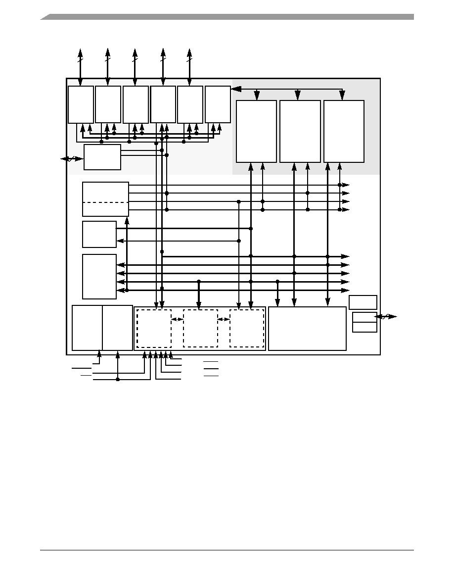
This manual describes the DSP56371 24-bit digital signal processor (DSP), its memory,
operating modes and peripheral modules. The DSP56371 is a member of the DSP56300
family of programmable CMOS DSPs. The DSP56371 is targeted to applications that
require digital audio compression/decompression, sound field processing, acoustic
equalization and other digital audio algorithms. Changes in core functionality specific to the
DSP56371 are also described in this manual. See
Figure 1.
for the block diagram of the
DSP56371.
Table of Contents
Section
Page
1 Introduction ................................... 1
2 DSP56371 Overview..................... 1
3 Signal/Connection Descriptions .... 8
4 Maximum Ratings ....................... 30
5 Power Requirements................... 32
6 Thermal Characteristics.............. 32
7 DC Electrical Characteristics ...... 33
8 AC Electrical Characteristics....... 34
9 Internal Clocks ............................ 34
10 External Clock Operation .......... 35
11 Reset, Stop, Mode Select, and
Interrupt Timing ........................... 36
12 Serial Host Interface SPI Protocol
Timing.......................................... 39
13 Serial Host Interface (SHI) I2C
Protocol Timing ........................... 44
14 Enhanced Serial Audio Interface
Timing.......................................... 46
15 Digital Audio Transmitter Timing51
16 Timer Timing ............................. 51
17 GPIO Timing ............................. 52
18 JTAG Timing ............................. 53
19 Package Information ................. 55
20 Design Considerations.............. 61
21 Power Consumption Benchmark63
22 IBIS Model ................................ 66
2
DSP56371 Technical Data
Freescale Semiconductor
DSP56371 Overview
Figure 1.
DSP56371 Block Diagram
2.2
DSP56300 Core Description
The DSP56371 uses the DSP56300 core, a high-performance, single clock cycle per instruction engine that provides up to twice
the performance of Motorola's popular DSP56000 core family while retaining code compatibility with it.
The DSP56300 core family offers a new level of performance in speed and power, provided by its rich instruction set and low
power dissipation, thus enabling a new generation of wireless, telecommunications and multimedia products. For a description
of the DSP56300 core, see
Section 2.4 DSP56300 Core Functional Blocks
. Significant architectural enhancements to the
DSP56300 core family include a barrel shifter, 24-bit addressing, an instruction patch module and direct memory access (DMA).
The DSP56300 core family members contain the DSP56300 core and additional modules. The modules are chosen from a library
of standard predesigned elements such as memories and peripherals. New modules may be added to the library to meet
customer specifications. A standard interface between the DSP56300 core and the on-chip memory and peripherals supports a
wide variety of memory and peripheral configurations. Refer to
DSP56371 User Manual, Section 3, Memory Configuration
.
Core features are described fully in the DSP56300 Family Manual. Pinout, memory and peripheral features are described in this
manual.
PLL
OnCETM
Clock
Gen-
erator
YAB
XAB
PAB
YDB
XDB
PDB
GDB
MODB/IRQB
MODC/IRQC
MODD/IRQD
DSP56300
12
24-Bit
DDB
DAB
Peripheral
Core
YM_EB
XM_EB
PM_EB
PIO
_
E
B
Expansion Area
JTAG
4
5
RESET
MODA/IRQA
PINIT/NMI
EXTAL
Address
Generation
Unit
Six Channel
DMA Unit
Program
Interrupt
Controller
Program
Decode
Controller
Program
Address
Generator
Data ALU
24
◊
24+56
56-bit MAC
Two 56-bit Accumulators
56-bit Barrel Shifter
Power
Mngmnt.
Memory Expansion Area
X Data
RAM
36K
◊
24
Y Data
RAM
48K
◊
24
Bootstrap
ROM
Internal
Data
Bus
Switch
SHI
Triple
ESAI
ESAI_1
EFCOP
Interface
Timer
Interface
Interface
12
2
GPIO
11
ROM
32K
◊
24
ROM
32K
◊
24
Program
RAM
4K
◊
24
ROM
64K
◊
24
DAX
2

DSP56371 Overview
Freescale Semiconductor
DSP56371 Technical Data
3
∑
DSP56300 modular chassis
--
181 Million Instructions Per Second (MIPS) with a 181 MHz clock at an internal logic supply (QVDDL) of 1.25V.
--
Object Code Compatible with the 56K core.
--
Data ALU with a 24 x 24 bit multiplier-accumulator and a 56-bit barrel shifter. 16-bit arithmetic support.
--
Program Control with position independent code support and instruction patch support.
--
EFCOP running concurrently with the core, capable of executing 181 million filter taps per second at peak
performance.
--
Six-channel DMA controller.
--
Low jitter, PLL based clocking with a wide range of frequency multiplications (1 to 255), predivider factors (1 to 31)
and power saving clock divider (2
i
: i=0 to 7). Reduces clock noise.
--
Internal address tracing support and OnCE for Hardware/Software debugging.
--
JTAG port.
--
Very low-power CMOS design, fully static design with operating frequencies down to DC.
--
STOP and WAIT low-power standby modes.
∑
On-chip Memory Configuration
--
48Kx24 Bit Y-Data RAM and 32Kx24 Bit Y-Data ROM.
--
36Kx24 Bit X-Data RAM and 32Kx24 Bit X-Data ROM.
--
64Kx24 Bit Program and Bootstrap ROM.
--
4Kx24 Bit Program RAM.
--
PROM patching mechanism.
--
Up to 32Kx24 Bit from Y Data RAM and 8Kx24 Bit from X Data RAM can be switched to Program RAM resulting in
up to 44Kx24 Bit of Program RAM.
∑
Peripheral modules
--
Enhanced Serial Audio Interface (ESAI): up to 4 receivers and up to 6 transmitters, master or slave. I
2
S, Left
justified, Right justified, Sony, AC97, network and other programmable protocols.
--
Enhanced Serial Audio Interface I (ESAI_1): up to 4 receivers and up to 6 transmitters, master or slave. I
2
S, Left
justified, Right justified, Sony, AC97, network and other programmable protocols.
--
Serial Host Interface (SHI): SPI and I
2
C protocols, multi master capability in I
2
C mode, 10-word receive FIFO,
support for 8, 16 and 24-bit words.
--
Triple Timer module (TEC).
--
11 dedicated GPIO pins
--
Digital Audio Transmitter (DAX): 1 serial transmitter capable of supporting the SPDIF, IEC958, CP-340 and
AES/EBU digital audio formats.
--
Pins of unused peripherals (except SHI) may be programmed as GPIO lines.
2.3
DSP56371 Audio Processor Architecture
This section defines the DSP56371 audio processor architecture. The audio processor is composed of the following units:
∑
The DSP56300 core is composed of the Data ALU, Address Generation Unit, Program Controller, DMA Controller,
Memory Module Interface, Peripheral Module Interface and the On-Chip Emulator (OnCE). The DSP56300 core is
described in the document
DSP56300 24-Bit Digital Signal Processor Family Manual, Motorola publication
DSP56300FM/AD
.
∑
Phased Lock Loop and Clock Generator
∑
Memory modules.
∑
Peripheral modules. The peripheral modules are defined in the following sections.
Memory sizes in the block diagram are defaults. Memory may be differently partitioned, according to the memory mode of the
chip. See
Section 2.4.7 On-Chip Memory
for more details about memory size.
2.4
DSP56300 Core Functional Blocks
The DSP56300 core provides the following functional blocks:
∑
Data arithmetic logic unit (Data ALU)
∑
Address generation unit (AGU)

4
DSP56371 Technical Data
Freescale Semiconductor
DSP56371 Overview
∑
Program control unit (PCU)
∑
DMA controller (with six channels)
∑
Instruction patch controller
∑
PLL-based clock oscillator
∑
OnCE module
∑
Memory
In addition, the DSP56371 provides a set of on-chip peripherals, described in
Section 2.5 Peripheral Overview
.
2.4.1 Data
ALU
The Data ALU performs all the arithmetic and logical operations on data operands in the DSP56300 core. The components of
the Data ALU are as follows:
∑
Fully pipelined 24-bit
◊ 24-bit parallel multiplier-accumulator (MAC)
∑
Bit field unit, comprising a 56-bit parallel barrel shifter (fast shift and normalization; bit stream generation and parsing)
∑
Conditional ALU instructions
∑
24-bit or 16-bit arithmetic support under software control
∑
Four 24-bit input general purpose registers: X1, X0, Y1 and Y0
∑
Six Data ALU registers (A2, A1, A0, B2, B1 and B0) that are concatenated into two general purpose, 56-bit accumulators
(A and B), accumulator shifters
∑
Two data bus shifter/limiter circuits
2.4.1.1
Data ALU Registers
The Data ALU registers can be read or written over the X memory data bus (XDB) and the Y memory data bus (YDB) as 24- or
48-bit operands (or as 16- or 32-bit operands in 16-bit arithmetic mode). The source operands for the Data ALU, which can be
24, 48, or 56 bits (16, 32, or 40 bits in 16-bit arithmetic mode), always originate from Data ALU registers. The results of all Data
ALU operations are stored in an accumulator.
All the Data ALU operations are performed in two clock cycles in pipeline fashion so that a new instruction can be initiated in
every clock, yielding an effective execution rate of one instruction per clock cycle. The destination of every arithmetic operation
can be used as a source operand for the immediately following arithmetic operation without a time penalty (i.e., without a pipeline
stall).
2.4.1.2
Multiplier-Accumulator (MAC)
The MAC unit comprises the main arithmetic processing unit of the DSP56300 core and performs all of the calculations on data
operands. In the case of arithmetic instructions, the unit accepts as many as three input operands and outputs one 56-bit result
of the following form- Extension:Most Significant Product:Least Significant Product (EXT:MSP:LSP).
The multiplier executes 24-bit
◊ 24-bit, parallel, fractional multiplies, between two's-complement signed, unsigned, or mixed
operands. The 48-bit product is right-justified and added to the 56-bit contents of either the A or B accumulator. A 56-bit result
can be stored as a 24-bit operand. The LSP can either be truncated or rounded into the MSP. Rounding is performed if specified.

DSP56371 Overview
Freescale Semiconductor
DSP56371 Technical Data
5
2.4.2
Address Generation Unit (AGU)
The AGU performs the effective address calculations using integer arithmetic necessary to address data operands in memory
and contains the registers used to generate the addresses. It implements four types of arithmetic: linear, modulo, multiple wrap-
around modulo and reverse-carry. The AGU operates in parallel with other chip resources to minimize address-generation
overhead.
The AGU is divided into two halves, each with its own Address ALU. Each Address ALU has four sets of register triplets, and
each register triplet is composed of an address register, an offset register and a modifier register. The two Address ALUs are
identical. Each contains a 24-bit full adder (called an offset adder).
A second full adder (called a modulo adder) adds the summed result of the first full adder to a modulo value that is stored in its
respective modifier register. A third full adder (called a reverse-carry adder) is also provided.
The offset adder and the reverse-carry adder are in parallel and share common inputs. The only difference between them is that
the carry propagates in opposite directions. Test logic determines which of the three summed results of the full adders is output.
Each Address ALU can update one address register from its respective address register file during one instruction cycle. The
contents of the associated modifier register specifies the type of arithmetic to be used in the address register update calculation.
The modifier value is decoded in the Address ALU.
2.4.3
Program Control Unit (PCU)
The PCU performs instruction prefetch, instruction decoding, hardware DO loop control and exception processing. The PCU
implements a seven-stage pipeline and controls the different processing states of the DSP56300 core. The PCU consists of the
following three hardware blocks:
∑
Program decode controller (PDC)
∑
Program address generator (PAG)
∑
Program interrupt controller
The PDC decodes the 24-bit instruction loaded into the instruction latch and generates all signals necessary for pipeline control.
The PAG contains all the hardware needed for program address generation, system stack and loop control. The Program
interrupt controller arbitrates among all interrupt requests (internal interrupts, as well as the five external requests: IRQA, IRQB,
IRQC, IRQD and NMI) and generates the appropriate interrupt vector address.
PCU features include the following:
∑
Position independent code support
∑
Addressing modes optimized for DSP applications (including immediate offsets)
∑
On-chip instruction cache controller
∑
On-chip memory-expandable hardware stack
∑
Nested hardware DO loops
∑
Fast auto-return interrupts
The PCU implements its functions using the following registers:
∑
PC--program counter register
∑
SR--Status register
∑
LA--loop address register
∑
LC--loop counter register
∑
VBA--vector base address register
∑
SZ--stack size register
∑
SP--stack pointer
∑
OMR--operating mode register
∑
SC--stack counter register
The PCU also includes a hardware system stack (SS).