 | –≠–ª–µ–∫—Ç—Ä–æ–Ω–Ω—ã–π –∫–æ–º–ø–æ–Ω–µ–Ω—Ç: FAN73832M | –°–∫–∞—á–∞—Ç—å:  PDF PDF  ZIP ZIP |
September 2006
F
AN73
832 Half-Bri
dge Gate-
D
rive IC
© 2006 Fairchild Semiconductor Corporation
www.fairchildsemi.com
FAN73832 Rev. 1.0.0
FAN73832
Half-Bridge Gate-Drive IC
Features
Floating Channel for Bootstrap Operation to +600V
Typically 350mA/650mA Sourcing/Sinking Current
Driving Capability for Both Channels
Extended Allowable Negative V
S
Swing to -9.8V for
Signal Propagation at V
DD
=V
BS
=15V
High-Side Output in Phase of IN Input Signal
Built-in UVLO Functions for Both Channels
Built-in Common-Mode dv/dt Noise Canceling Circuit
Internal 400nsec Minimum Dead-Time at R
DT
=20K
Programmable Turn-on Delay-Time Control
(Dead-Time)
Applications
SMPS
Motor Drive Inverter
Fluorescent Lamp Ballast
HID Ballast
Description
The FAN73832 is a half-bridge, gate-drive IC with shut-
down and programmable dead-time control functions for
driving MOSFETs and IGBTs, operating up to +600V.
Fairchild's high-voltage process and common-mode
noise canceling technique provide stable operation of
high-side driver under high dv/dt noise circumstances.
An advanced level-shift circuit allows high-side gate
driver operation up to V
S
=-9.8V (typical) for V
BS
=15V.
The UVLO circuits for both channels prevent malfunction
when V
DD
and V
BS
are lower than the specified thresh-
old voltage.
Output drivers typically source/sink 350mA/650mA,
respectively, which is suitable for all kinds of half- and
full-bridge inverters.
Ordering Information
Note:
1. These devices passed wave soldering test by JESD22A-111.
8 SOP
8-DIP
Part Number
Package
Pb-Free
Operating Temperature Range Packing Method
FAN73832M
(1)
8-SOP
Yes
-40∞C ~ 125∞C
Tube
FAN73832MX
(1)
Tape & Reel
FAN73832N
8-DIP
Tube

F
AN73
832 Ha
lf-B
ridge Ga
te-Drive IC
© 2006 Fairchild Semiconductor Corporation
www.fairchildsemi.com
FAN73832 Rev. 1.0.0
2
Typical Application Diagrams
Figure 1. Application Circuit for Half-Bridge Switching Power Supply
Figure 2. Application Circuit for Full-Bridge DC Motor Driver
V
DD
V
DC
PWM IC
PWM
Shutdown
Control
1
3
2
V
DD
LO
V
B
V
S
HO
GND
IN
4
FAN73832
8
5
6
7
R
DT
D
BOOT
C
BOOT
DT/ SD
FAN73832 Rev:00
HO
V
S
V
B
V
DD
GND
IN
FAN73832
V
DC
V
CC
DC Motor
Controller
PHA
PHB
LO
SD
DT/ SD
Forward
M
Reverse
HO
V
S
V
B
V
DD
GND
IN
FAN73832
LO
DT/ SD
FAN73832 Rev:00

F
AN73
832 Ha
lf-B
ridge Ga
te-Drive IC
© 2006 Fairchild Semiconductor Corporation
www.fairchildsemi.com
FAN73832 Rev. 1.0.0
3
Internal Block Diagram
Figure 3. Functional Block Diagram of FAN73832
UVLO
DR
I
V
ER
PU
L
S
E
GE
N
E
R
A
T
OR
3
1
4
2
8
6
IN
V
DD
GND
LO
V
B
HO
V
S
R
R
S
Q
DR
I
V
E
R
HS(ON/ OFF)
LS(ON/ OFF)
DELAY
UVLO
SCHMITT
TRIGGER INPUT
DEAD - TIME
NOISE
CANCELLER
5
7
DT/SD
R
DTINT
CONTROL
FAN73832 Rev:00
F
AN73
832 Ha
lf-B
ridge Ga
te-Drive IC
© 2006 Fairchild Semiconductor Corporation
www.fairchildsemi.com
FAN73832 Rev. 1.0.0
4
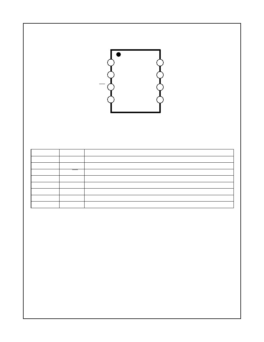
Pin Assignments
Figure 4. Pin Configuration (Top View)
Pin Definitions
Pin #
Name
Description
1
IN
Logic Input
2
GND
Ground
3
DT/SD
Dead-Time Control with External Resistor and Shutdown Function
4
V
DD
Low-Side Supply Voltage
5
LO
Low-Side Driver Output
6
V
S
High-Side Floating Supply Return
7
HO
High-Side Driver Output
8
V
B
High-Side Floating Supply
LO
IN
V
DD
V
S
HO
V
B
GND
1
2
3
4
8
7
6
5
F
AN73832
DT/SD
FAN73832 Rev:00
F
AN73
832 Ha
lf-B
ridge Ga
te-Drive IC
© 2006 Fairchild Semiconductor Corporation
www.fairchildsemi.com
FAN73832 Rev. 1.0.0
5
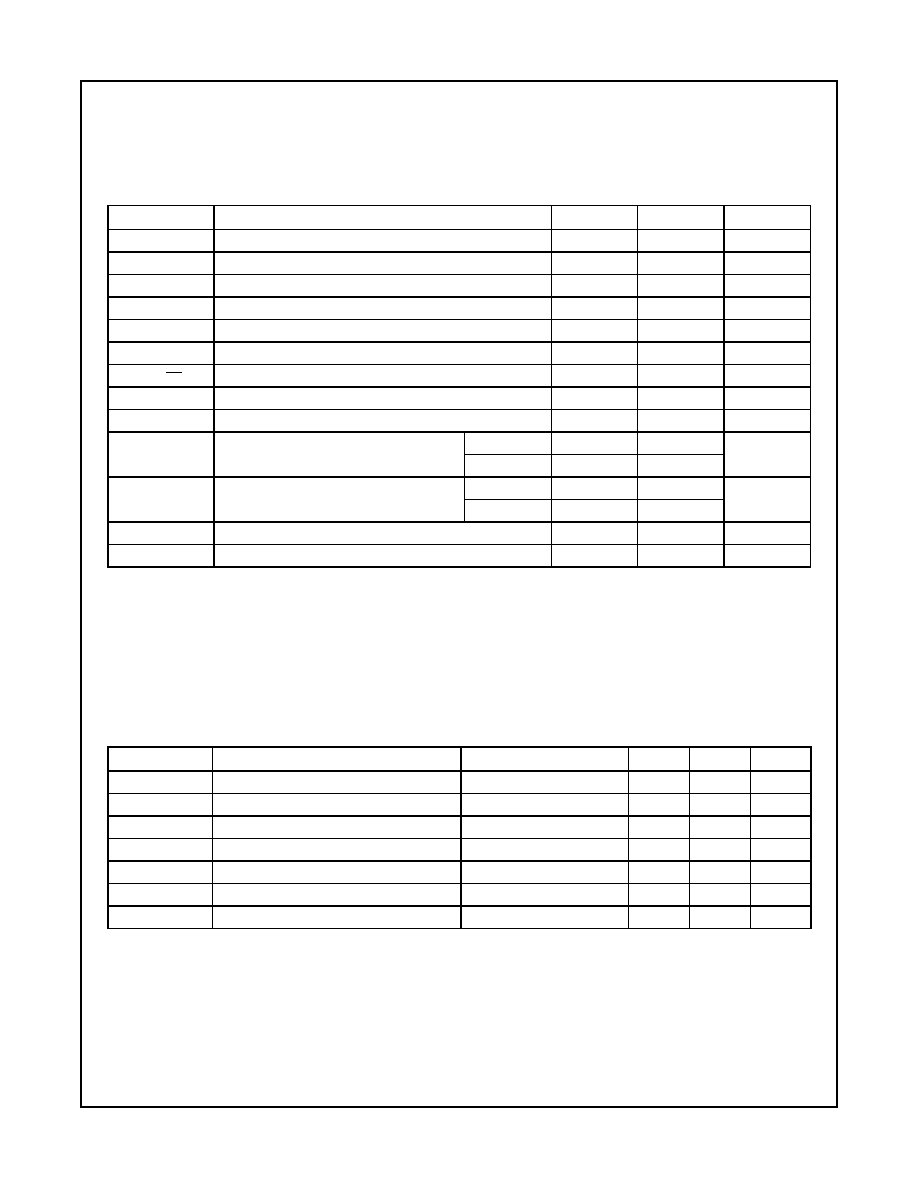
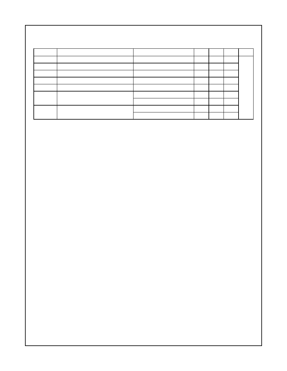
Absolute Maximum Ratings
The "Absolute Maximum Ratings" are those values beyond which the safety of the device cannot be guaranteed. The
device should not be operated at these limits. The parametric values defined in the Electrical Characteristics tables are
not guaranteed at the absolute maximum ratings. The "Recommended Operating Conditions" table defines the condi-
tions for actual device operation. T
A
=25∞C unless otherwise specified.
Notes:
2. Mounted on 76.2 x 114.3 x 1.6mm PCB (FR-4 glass epoxy material).
3. Refer to the following standards:
JESD51-2: Integral circuits thermal test method environmental conditions - Natural convection
JESD51-3: Low effective thermal conductivity test board for leaded surface mount packages
4. Do not exceed P
D
under any circumstances.
Recommended Operating Conditions
Symbol
Characteristics
Min.
Max.
Unit
V
S
High-side offset voltage
V
B
-25
V
B
+0.3
V
V
B
High-side floating supply voltage
-0.3
625
V
V
HO
High-side floating output voltage HO
V
S
-0.3
V
B
+0.3
V
V
DD
Low-side and logic-fixed supply voltage
-0.3
25
V
V
LO
Low-side output voltage LO
-0.3
V
DD
+0.3
V
V
IN
Logic input voltage (IN)
-0.3
V
DD
+0.3
V
V
DT/SD
Dead-time and shutdown control voltage
-0.3
5.0
V
GND
Logic ground
V
DD
-25
V
DD
+0.3
V
dV
S
/dt
Allowable offset voltage slew rate
50
V/nsec
P
D
(2)(3)(4)
Power dissipation
8-SOP
0.625
W
8-DIP
1.25
JA
Thermal resistance, junction-to-ambient
8-SOP
200
∞
C/W
8-DIP
100
T
J
Junction temperature
150
∞
C
T
STG
Storage temperature
150
∞
C
Symbol
Parameter
Condition
Min.
Max.
Unit
V
B
High-side floating supply voltage
V
S
+15
V
S
+20
V
V
S
High-side floating supply offset voltage
6-V
DD
600
V
V
DD
Low-side supply voltage
15
20
V
V
HO
High-side (HO) output voltage
V
S
V
B
V
V
LO
Low-side (LO) output voltage
GND
V
DD
V
V
IN
Logic input voltage (IN)
GND
V
DD
V
T
A
Ambient temperature
-40
125
∞
C
F
AN73
832 Ha
lf-B
ridge Ga
te-Drive IC
© 2006 Fairchild Semiconductor Corporation
www.fairchildsemi.com
FAN73832 Rev. 1.0.0
6
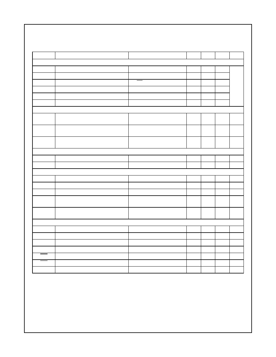
Electrical Characteristics
V
BIAS
(V
DD
, V
BS
)=15.0V, R
DT
=20K
,
T
A
=25
∞
C, unless otherwise specified. The V
IN
and I
IN
parameters are referenced
to GND. The V
O
and I
O
parameters are referenced to GND and V
S
is applicable to HO and LO.
Note:
4.
This parameter, although guaranteed, is not 100% tested in production.
Symbol
Characteristics
Test Condition
Min. Typ. Max. Unit
SUPPLY CURRENT SECTION
I
QBS
Quiescent V
BS
supply current
V
IN
=0V or 5V
35
90
µA
I
QDD
Quiescent V
DD
supply current
V
IN
=0V or 5V, R
DT
=20K
300
450
I
SD
(4)
Shutdown supply current
DT/
SD
=GND
650
900
I
PBS
Operating V
BS
supply current
f
IN
=20kHz, rms value
400
700
I
PDD
Operating V
DD
supply current
f
IN
=20kHz, rms value
650
850
I
LK
Offset supply leakage current
V
B
=V
S
=600V
10
POWER SUPPLY SECTION
V
DDUV+
V
BSUV+
V
DD
and V
BS
supply under-voltage
positive going threshold
10.7
11.6
12.5
V
V
DDUV-
V
BSUV-
V
DD
and V
BS
supply under-voltage
negative going threshold
10.0
10.8
11.6
V
V
DDUVH
V
BSUVH
V
DD
supply under-voltage lockout
hysteresis
0.8
V
DEAD-TIME CONTROL SECTION
R
DTINT
Internal dead-time setting resistance
20
K
V
DT
Normal voltage at DT
R
DT
=20K
3.0
V
GATE DRIVER OUTPUT SECTION
V
OH
High-level output voltage, V
BIAS
-V
O
I
O
=20mA
1.0
V
V
OL
Low-level output voltage, V
O
0.6
V
I
O+
Output high short-circuit pulse current
V
O
=0V, V
IN
=5V with PW<10µs
250
350
mA
I
O-
Output low short-circuit pulsed current
V
O
=15V,
V
IN
=0V with PW<10µs
500
650
mA
V
S
Allowable negative V
S
pin voltage for
IN signal propagation to HO
-9.8
-7.0
V
LOGIC INPUT SECTION (INPUT and SHUTDOWN)
V
IH
Logic "1" input voltage
2.9
V
V
IL
Logic "0" input voltage
1.2
V
I
IN+
Logic "1" input bias current
V
IN
=5V
50
100
µA
I
IN-
Logic "0" input bias current
V
IN
=0V
2.0
µA
SD+
Shutdown "1" input voltage
1.2
V
SD-
Shutdown "0" input voltage
2.9
V
R
PD
Input pull-down resistance
100
K
F
AN73
832 Ha
lf-B
ridge Ga
te-Drive IC
© 2006 Fairchild Semiconductor Corporation
www.fairchildsemi.com
FAN73832 Rev. 1.0.0
7
Dynamic Electrical Characteristics
V
BIAS
(V
DD
, V
BS
)=15.0V, V
S
=GND, C
L
=1000pF, R
DT
=20K
and T
A
= 25
∞
C, unless otherwise specified.
Note:
5.
This parameter, although guaranteed, is not 100% tested in production.
Symbol
Parameter
Conditions
Min. Typ. Max. Unit
t
ON
Turn-on propagation delay
V
S
=0V, R
DT
=20K
580
730
nsec
t
OFF
Turn-off propagation delay
V
S
=0V, R
DT
=20K
180
230
t
R
Turn-on rise time
C
L
=1000pF
50
100
t
F
Turn-off fall time
C
L
=1000pF
30
80
t
SD
(5)
Shutdown propagation delay
100
180
DT1, DT2
Dead-time LO OFF to HO ON & HO
OFF to LO ON
R
DT
=20K
300
400
500
R
DT
= 200K
1.20
1.68
2.30
DMT
Dead-time matching
R
DT
= 20K
0
60
R
DT
=200K
0
150

F
AN73
832 Ha
lf-B
ridge Ga
te-Drive IC
© 2006 Fairchild Semiconductor Corporation
www.fairchildsemi.com
FAN73832 Rev. 1.0.0
8
Typical Characteristics
Figure 5. V
DD
/
V
DD
UVLO (+) vs. Temperature
Figure 6. V
DD
/
V
BS
UVLO (-) vs. Temperature
Figure 7. V
DD
Quiescent Current vs. Temperature
Figure 8. V
BS
Quiescent Current vs. Temperature
Figure 9. V
DD
Operating Current vs. Temperature
Figure 10. V
BS
Operating Current vs. Temperature
-40
-20
0
20
40
60
80
100
120
10.8
11.0
11.2
11.4
11.6
11.8
12.0
V
DD
UV
+
,V
BS
U
V
+
[V
]
Temperature [∞C]
-40
-20
0
20
40
60
80
100
120
10.0
10.2
10.4
10.6
10.8
11.0
11.2
11.4
11.6
V
DD
UV-
,V
BS
U
V
-
[V]
Temperature [∞C]
-40
-20
0
20
40
60
80
100
120
0
100
200
300
400
500
I
QD
D
[
A]
Temperature [∞C]
-40
-20
0
20
40
60
80
100
120
0
20
40
60
80
100
I
QB
S
[
A]
Temperature [∞C]
-40
-20
0
20
40
60
80
100
120
0
200
400
600
800
1000
I
PD
D
[
A]
Temperature [∞C]
-40
-20
0
20
40
60
80
100
120
0
200
400
600
800
I
PB
S
[
A]
Temperature [∞C]

F
AN73
832 Ha
lf-B
ridge Ga
te-Drive IC
© 2006 Fairchild Semiconductor Corporation
www.fairchildsemi.com
FAN73832 Rev. 1.0.0
9
Typical Characteristics
(Continued)
Figure 11. Logic Input Current vs. Temperature
Figure 12. Logic Input High Voltage vs. Temperature
Figure 13. Logic Input Low Voltage vs. Temperature
Figure 14. SD Positive Threshold vs. Temperature
Figure 15. SD Negative Threshold vs. Temperature
Figure 16. Turn-on Delay Time vs. Temperature
-40
-20
0
20
40
60
80
100
120
0
20
40
60
80
100
I
IN+
[
A]
Temperature [∞C]
-40
-20
0
20
40
60
80
100
120
0.0
0.5
1.0
1.5
2.0
2.5
3.0
V
IH
[V
]
Temperature [∞C]
-40
-20
0
20
40
60
80
100
120
0.0
0.5
1.0
1.5
2.0
2.5
3.0
V
IL
[V
]
Temperature [∞C]
-40
-20
0
20
40
60
80
100
120
0.0
0.5
1.0
1.5
2.0
2.5
3.0
SD+
BA
R
[V
]
Temperature [∞C]
-40
-20
0
20
40
60
80
100
120
0.0
0.5
1.0
1.5
2.0
2.5
3.0
SD-
BAR
[V
]
Temperature [∞C]
-40
-20
0
20
40
60
80
100
120
0
200
400
600
800
t
ON
[
n
se
c]
Temperature [∞C]
F
AN73
832 Ha
lf-B
ridge Ga
te-Drive IC
© 2006 Fairchild Semiconductor Corporation
www.fairchildsemi.com
FAN73832 Rev. 1.0.0
10
Typical Characteristics
(Continued)
Figure 17. Turn-off Delay Time vs. Temperature
Figure 18. Dead Time (R
DT
=20k) vs. Temperature
Figure 19. Dead Time (R
DT
=200k) vs. Temperature
Figure 20. R
DT
vs. Dead Time
Figure 21. Allowable Negative V
S
Voltage for Signal
Propagation to High Side vs. Temperature
-40
-20
0
20
40
60
80
100
120
0
50
100
150
200
250
300
t
OF
F
[n
s
e
c
]
Temperature [∞C]
-40
-20
0
20
40
60
80
100
120
300
350
400
450
500
D
T1
, R
DT
= 20k
[ns
e
c
]
Temperature [∞C]
-40
-20
0
20
40
60
80
100
120
1.2
1.4
1.6
1.8
2.0
2.2
2.4
D
T1
, R
DT
= 200k
[
nsec]
Temperature [∞C]
20
40
60
80
100
120
140
160
180
200
0.0
0.4
0.8
1.2
1.6
2.0
D
e
ad
time
[
S]
RDT [kohm]
-40
-20
0
20
40
60
80
100
120
-14
-12
-10
-8
-6
V
S
[V
]
Temperature [∞C]
F
AN73
832 Ha
lf-B
ridge Ga
te-Drive IC
© 2006 Fairchild Semiconductor Corporation
www.fairchildsemi.com
FAN73832 Rev. 1.0.0
11
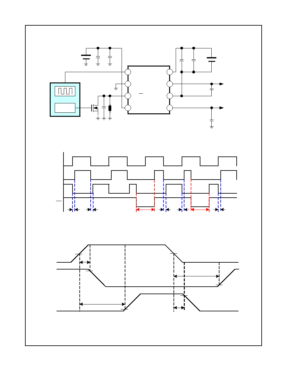
Switching Time Definitions
Figure 22. Switching Time Test Circuit
Figure 23. Input / Output Waveforms
Figure 24. Switching Time Waveform Definitions
+15V
SD
1
3
2
GND
LO
V
B
V
S
HO
V
DD
DT/SD
IN
4
FAN73832
5
6
7
10
F 100nF
20K
1nF
1nF
+15V
100nF
10
F
Control
8
HO
LO
FAN73832 Rev:00
IN
HO
LO
DT/SD
DT1
DT2
DT1
DT2
DT1
Shutdown
Shutdown
FAN73832 Rev.00
IN
HO
LO
10%
90%
50%
50%
90%
10%
t
OFF
t
OFF
t
ON
t
ON
FAN73832 Rev.00
F
AN73
832 Ha
lf-B
ridge Ga
te-Drive IC
© 2006 Fairchild Semiconductor Corporation
www.fairchildsemi.com
FAN73832 Rev. 1.0.0
12
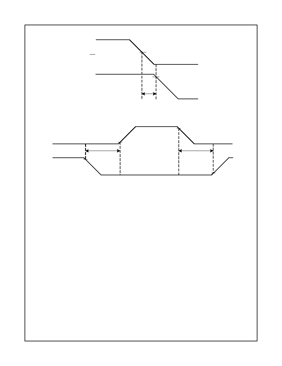
Figure 25. Shutdown Waveform Definition
Figure 26. Dead-Time Control Waveform Definition
90%
50%
t
SD
HO or LO
DT/SD
FAN73832 Rev.00
HO
10%
90%
DT1
LO
90%
10%
DT2
MDT=
|
DT1 - DT2
|
FAN73832 Rev.00

F
AN73
832 Ha
lf-B
ridge Ga
te-Drive IC
© 2006 Fairchild Semiconductor Corporation
www.fairchildsemi.com
FAN73832 Rev. 1.0.0
13
Typical Application Information
1. Normal Operating Consideration
The FAN73832 is a single PWM input, half-bridge, gate-
drive IC with programmable dead-time and shutdown
functions.
The dead-time is set with a resistor (R
DT
) at the DT/SD
pin. The wide dead-time programming range provides
the flexibility to optimize drive signal timing for a
selection of switching devices (MOSFET or IGBT) and
applications.
The turn-on time delay circuitry (Dead-Time)
accommodates resistor values from 20k
to 200k
with
a dead-time proportional to the R
DT
resistance.
If the DT/SD pin voltage decreases below 1.2V in the
normal operation, the IC enters shutdown mode.
The external dead-time setting resistor (R
DT
) is at least
above 20K
for normal operation in typical applications.
2. Under Voltage Lockout (UVLO)
The FAN73832 has an under-voltage lockout (UVLO)
protection circuit for high- and low-side channels to
prevent malfunction when V
DD
and V
BS
are lower than
the specified threshold voltage. The UVLO circuitry
monitors the supply voltage (V
DD
) and bootstrap
capacitor voltage (V
BS
) indepently.
3. Layout Consideration
For optimum performance of the high- and low-side gate
drivers, considerations must be taken during printed
circuit board (PCB) layout.
3.1 Supply Capacitors
If the output stages are able to quickly turn-on a
switching device with a high value of current, the supply
capacitors must be placed as close as possible to the
device pins (V
DD
and GND for the ground-tied supply, V
B
and V
S
for the floating supply) to minimize parasitic
inductance and resistance.
3.2 Gate Drive Loop
Current loops behave like an antenna, able to receive
and transmit noise. To reduce the noise coupling/emis-
sion and improve the power switch turn-on and off per-
formances, gate drive loops must be reduced as much
as possible.
3.3 Ground Plane
Ground plane must not be placed under or nearby the
high-voltage floating side to minimize noise coupling.
F
AN73
832 Ha
lf-B
ridge Ga
te-Drive IC
© 2006 Fairchild Semiconductor Corporation
www.fairchildsemi.com
FAN73832 Rev. 1.0.0
14
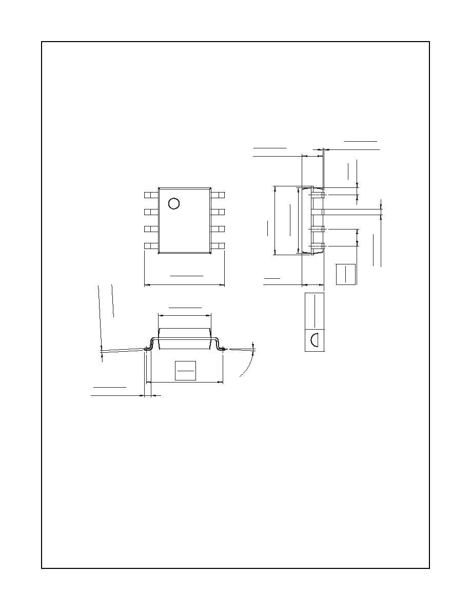
Mechanical Dimensions
8-SOP
Dimensions are in millimeters (inches) unless otherwise noted..
January 2001, Rev. A
4.92
±
0.20
0.194
±
0.008
0.41
±
0.10
0.016
±
0.004
1.27
0.050
5.72
0.225
1.55
±0.20
0.061
±0.008
0.1~0.25
0.004~0.001
6.00
±0.30
0.236
±0.012
3.95
±0.20
0.156
±0.008
0.50
±0.20
0.020
±0.008
5.13
0.202
MAX
#1
#4
#5
0~8
∞
#8
0.56
0.022
()
1.80
0.071
MAX0.10
MAX0.004
MAX
MIN
+
0.10
-0.05
0.15
+
0.004
-0.002
0.0
06
8sop225_dim.pdf
F
AN73
832 Ha
lf-B
ridge Ga
te-Drive IC
© 2006 Fairchild Semiconductor Corporation
www.fairchildsemi.com
FAN73832 Rev. 1.0.0
15
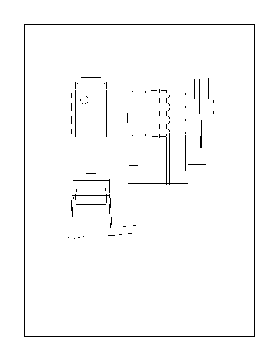
Mechanical Dimensions
(Continued)
8-DIP
Dimensions are in millimeters (inches) unless otherwise noted..
September 1999, Rev B
6.40
±0.20
3.30
±0.30
0.130
±0.012
3.40
±0.20
0.134
±0.008
#1
#4
#5
#8
0.252
±0.008
9.20
±
0.20
0.79
2.54
0.100
0.031
()
0.46
±
0.10
0.018
±
0.004
0.060
±
0.004
1.524
±
0.10
0.362
±
0.008
9.60 0.378
MAX
5.08
0.200
0.33
0.013
7.62
0~15∞
0.300
MAX
MIN
0.25
+0.10
≠0.05
0.010
+0.004
≠0.002
pdip8_dim.pdf

TRADEMARKS
The following are registered and unregistered trademarks Fairchild Semiconductor owns or is authorized to use and is not intended to be an
exhaustive list of all such trademarks.
ACEx GlobalOptoisolator
OCXPro
SerDes
TinyBuck
ActiveArray
GTO
OPTOLOGIC
Æ
SILENT
SWITCHER
Æ
TinyLogic
Æ
Bottomless
HiSeC
OPTOPLANAR SMART
START TINYOPTO
Build it Now
I
2
C
PACMAN SPM TinyPower
CoolFET
i-Lo
POP Stealth TinyPWM
CROSSVOLT
ImpliedDisconnect
Power247 SuperFET TruTranslation
DOME
IntelliMAX
PowerEdge SuperSOT -3 UHC
EcoSPARK
ISOPLANAR
PowerSaver
SuperSOT -6
UltraFET
Æ
E
2
CMOS
LittleFET
PowerTrench
Æ
SuperSOT -8 UniFET
EnSigna
MICROCOUPLER
QFET
Æ
SyncFET VCX
FACT
MicroFET QS TCM Wire
FACT Quiet Series
MicroPak QT
Optoelectronics TinyBoost
FAST
Æ
MICROWIRE Quiet
Series
FASTr
MSX RapidConfigure
Across the board. Around the world.
FPS
MSXPro RapidConnect
Programmable Active Droop
FRFET
OCX ScalarPump
The Power Franchise
Æ
DISCLAIMER
FAIRCHILD SEMICONDUCTOR RESERVES THE RIGHT TO MAKE CHANGES WITHOUT FURTHER NOTICE TO ANY PRODUCTS
HEREIN TO IMPROVE RELIABILITY, FUNCTION OR DESIGN. FAIRCHILD DOES NOT ASSUME ANY LIABILITY ARISING OUT OF THE
APPLICATION OR USE OF ANY PRODUCT OR CIRCUIT DESCRIBED HEREIN; NEITHER DOES IT CONVEY ANY LICENSE UNDER
ITS PATENT RIGHTS, NOR THE RIGHTS OF OTHERS. THESE SPECIFICATIONS DO NOT EXPAND THE TERMS OF FAIRCHILD'S
WORLDWIDE TERMS AND CONDITIONS, SPECIFICALLY THE WARRANTY THEREIN, WHICH COVERS THESE PRODUCTS.
LIFE SUPPORT POLICY
FAIRCHILD'S PRODUCTS ARE NOT AUTHORIZED FOR USE AS CRITICAL COMPONENTS IN LIFE SUPPORT DEVICES OR
SYSTEMS WITHOUT THE EXPRESS WRITTEN APPROVAL OF FAIRCHILD SEMICONDUCTOR CORPORATION.
As used herein:
1.
Life support devices or systems are devices or systems
which, (a) are intended for surgical implant into the body or
(b) support or sustain life, and (c) whose failure to perform
when properly used in accordance with instructions for use
provided in the labeling, can be reasonably expected to
result in a significant injury of the user.
2.
A critical component in any component of a life support,
device, or system whose failure to perform can be
reasonably expected to cause the failure of the life
support device or system, or to affect its safety or
effectiveness.
PRODUCT STATUS DEFINITIONS
Definition of Terms
Datasheet Identification
Product Status
Definition
Advance Information
Formative or In
Design
This datasheet contains the design specifications for product
development. Specifications may change in any manner without
notice.
Preliminary
First Production
This datasheet contains preliminary data; supplementary data will
be published at a later date. Fairchild Semiconductor reserves the
right to make changes at any time without notice to improve design.
No Identification Needed
Full Production
This datasheet contains final specifications. Fairchild
Semiconductor reserves the right to make changes at any time
without notice to improve design.
Obsolete
Not In Production
This datasheet contains specifications on a product that has been
discontinued by Fairchild Semiconductor. The datasheet is printed
for reference information only.
Rev. I20
F
AN73
832 Ha
lf-B
ridge Ga
te-Drive IC
© 2006 Fairchild Semiconductor Corporation
www.fairchildsemi.com
FAN73832 Rev. 1.0.0
16