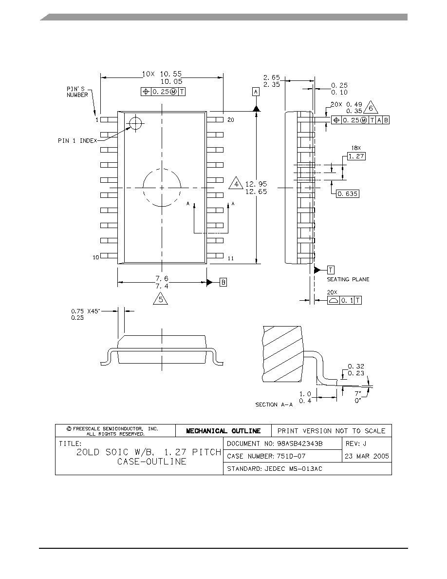
Document Number: MC100ES6017
Rev 2, 09/2005
Freescale Semiconductor
Technical Data
© Freescale Semiconductor, Inc., 2005. All rights reserved.
3.3 V ECL/PECL Quad Differential
Receiver
The MC100ES6017 is a 3.3 V ECL/PECL quad differential receiver. Under
open input conditions, the D input will be biased at V
CC
/2 and the D input will be
pulled down to V
EE
. This operation will force the Q output LOW and ensure
stability.
For single-ended input conditions, the unused differential input is connected
to V
BB
as a switching reference voltage. V
BB
may also rebias AC coupled inputs.
When used, decouple V
BB
and V
CC
via a 0.01
µF capacitor and limit current
sourcing or sinking to 0.5 mA. When not used, V
BB
should be left open.
Features
∑
High bandwidth output transitions
∑
LVPECL operating range: V
CC
= 3.0 V to 3.6 V
∑
Internal input pulldown resistors on D inputs, pullup and pulldown resistors on
D inputs
∑
20 lead SOIC package
∑
Ambient temperature range -40∞C to +85∞C
∑
20-lead Pb-free package available
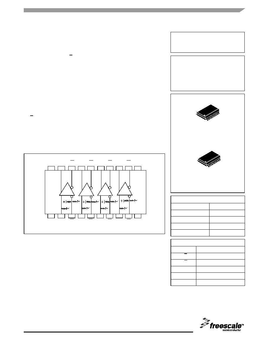
MC100ES6017
ECL/PECL QUAD
DIFFERENTIAL RECEIVER
DW SUFFIX
20-LEAD SOIC PACKAGE
CASE 751D-07
ORDERING INFORMATION
Device
Package
MC100ES6017DW
SO-20
MC100ES6017DWR2
SO-20
MC100ES6017EG
SO-20 (Pb-Free)
MC100ES6017EGR2
SO-20 (Pb-Free)
PIN DESCRIPTION
Pin
Function
Dn, Dn
ECL Differential Data Inputs
Qn, Qn
ECL Differential Data Outputs
V
BB
Reference Voltage Output
V
CC
Positive Supply
V
EE
Negative Supply
EG SUFFIX
20-LEAD SOIC PACKAGE
Pb-FREE PACKAGE
CASE 751D-07
Figure 1. 20-Lead Pinout (Top View) and Logic Diagram
1
20
19
18
17
16
15
14
13
2
3
6
V
CC
V
CC
D0
D0
D1
D1
Q0
Q3
Q1
Q0
Q2
Q2
4
Q1
5
7
8
D2
D3
V
BB
9
10
12
11
V
EE
Q3
D2
D3
Advanced Clock Drivers Device Data
2
Freescale Semiconductor
MC100ES6017
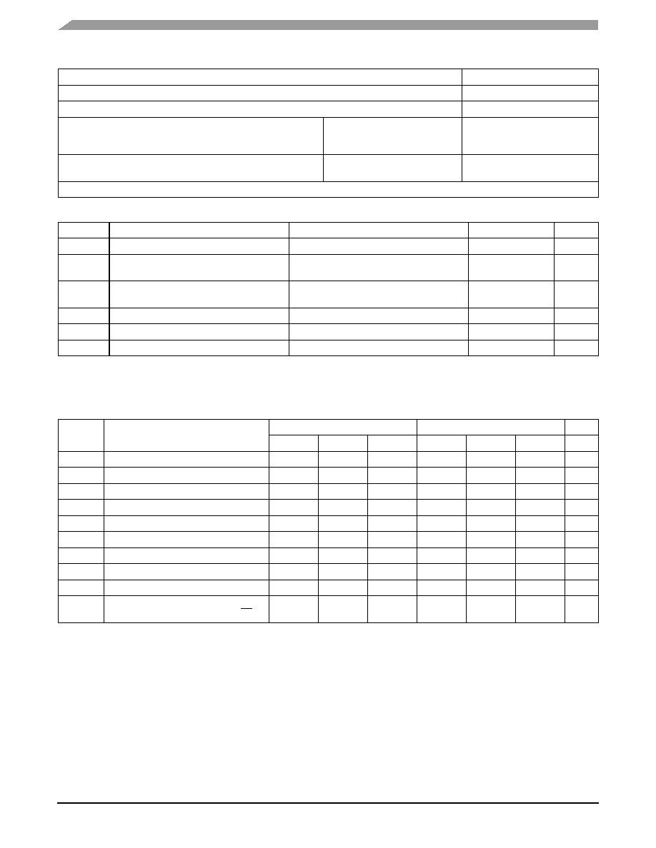
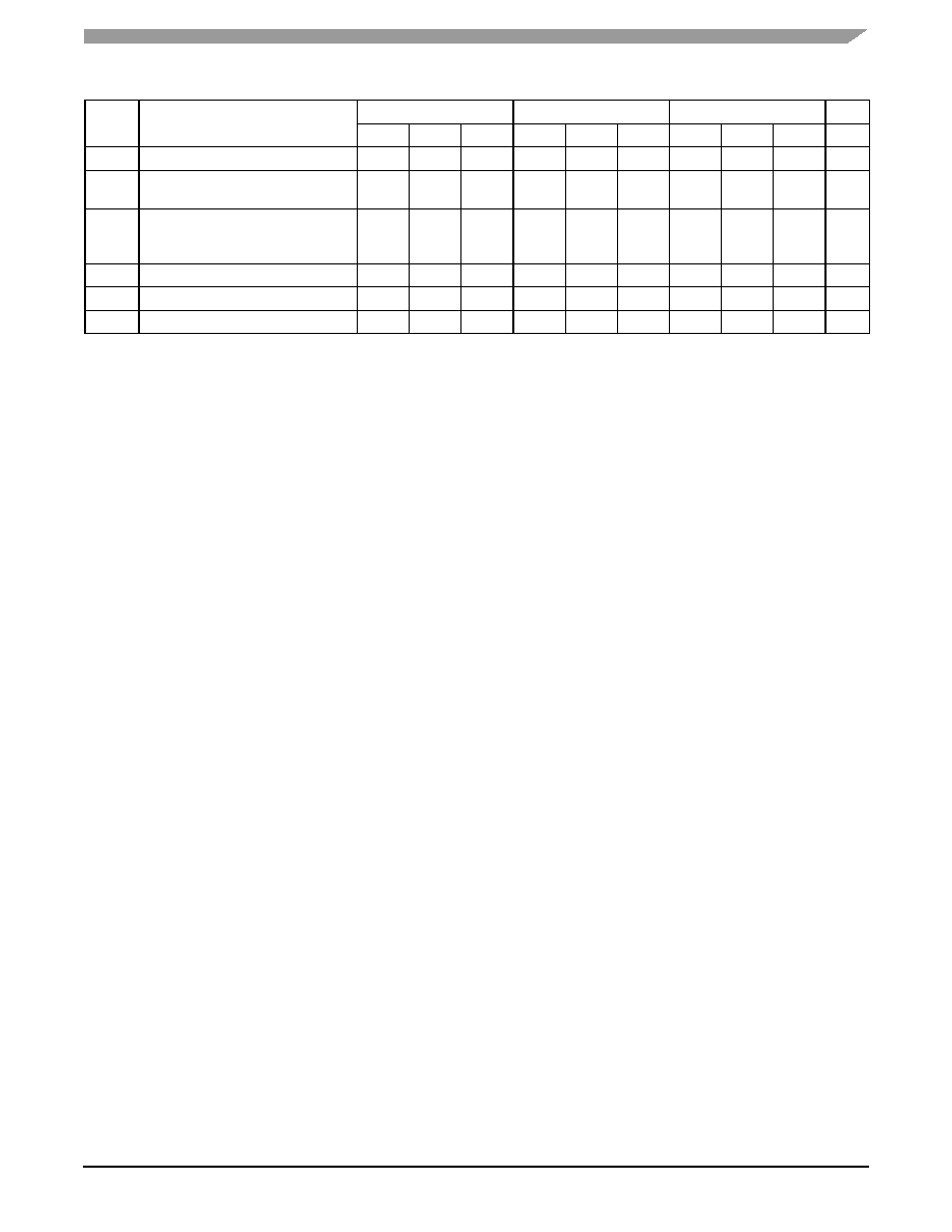
Table 1. General Specifications
Characteristics
Value
Internal Input Pulldown Resistor
75 k
Internal Input Pullup Resistor
75 k
ESD Protection
Human Body Model
Machine Model
Charged Device Model
> 2000 V
> 200 V
> 1500 V
JA
Thermal Resistance (Junction to Ambient)
0 LFPM, 20 SOIC
500 LFPM, 20 SOIC
90 ∞C/W
60 ∞C/W
Meets or exceeds JEDEC Spec EIA/JESD78 IC Latchup Test
Table 2. Absolute Maximum Ratings
(1)
1. Absolute maximum continuous ratings are those maximum values beyond which damage to the device may occur. Exposure to these
conditions or conditions beyond those indicated may adversely affect device reliability. Functional operation at absolute-maximum-rated
conditions is not implied.
Symbol
Parameter
Conditions
Rating
Unit
V
SUPPLY
Power Supply Voltage
difference between V
CC
& V
EE
3.9
V
V
IN
Input Voltage
V
CC
- V
EE
3.6 V
V
CC
+ 0.3
V
EE
- 0.3
V
V
I
OUT
Output Current
Continuous
Surge
50
100
mA
mA
I
BB
V
BB
Sink/Source
± 0.5
mA
TA
Operating Temp Range
-40 to +85
∞C
T
STG
Storage Temp Range
-65 to +150
∞C
Table 3. DC Characteristics (V
CC
= 3.0 to 3.6 V; V
EE
= 0 V or V
CC
= 0 V; V
EE
= -3.6 to -3.0 V)
-40∞C
0∞C to 85∞C
Symbol
Characteristic
Min
Typ
Max
Min
Typ
Max
Unit
I
EE
Power Supply Current
20
31
28
35
mA
V
OH
(1)
1. Outputs are terminated through a 50
resistor to V
CC
-2 volts.
Output HIGH Voltage
V
CC
- 1150 V
CC
- 1020
V
CC
- 800
V
CC
- 1200
V
CC
- 970
V
CC
- 750
mV
V
OL
(1)
Output LOW Voltage
V
CC
- 1950 V
CC
- 1620 V
CC
- 1250 V
CC
- 2000 V
CC
- 1680 V
CC
- 1300
mV
V
IH
Input HIGH Voltage
V
CC
- 1165
V
CC
- 880
V
CC
- 1165
V
CC
- 880
mV
V
IL
Input LOW Voltage
V
CC
- 1810
V
CC
- 1475 V
CC
- 1810
V
CC
- 1475
mV
V
BB
(2)
2. Input swing is centered around V
BB
.
Output Voltage Reference (I
BB
= 0.5 mA)
V
CC
- 1440
V
CC
- 1235 V
CC
- 1440
V
CC
- 1235
mV
V
PP
Differential Input Votage
0.12
1.3
0.12
1.3
V
V
CMR
Differential Cross Point Voltage
V
EE
+ 1.3
V
CC
- 0.9
V
EE
+ 1.3
V
CC
- 0.9
V
I
IH
Input HIGH Current
150
150
µA
I
IL
Input LOW Current
Dn
Dn
0.5
-300
0.5
-300
µA
µA
Advanced Clock Drivers Device Data
Freescale Semiconductor
3
MC100ES6017
Table 4. AC Characteristics (V
CC
= 3.0 to 3.6 V; V
EE
= 0 V or V
CC
= 0 V; V
EE
= -3.6 to -3.0 V)
-40∞C
25∞C
85∞C
Symbol
Characteristic
Min
Typ
Max
Min
Typ
Max
Min
Typ
Max
Unit
f
max
Maximum Toggle Frequency
1.75
1.75
1.75
GHz
t
PLH
,
t
PHL
Propagation Delay to Output
Diff
S.E.
(1)
1. Single-ended input propagation delay requires t
r
and t
f
350 ps to meet specified propagation delay. Device will function with larger t
r
and t
f
values.
310
225
510
595
310
225
510
595
310
225
510
595
ps
t
SKEW
Data Path Skew
(2)
(differential)
Part-to-Part Skew
(2)
(differential)
Pulse Width Skew
(2)
(3)
(differential)
2. Skews are valid across specified voltage range, part-to-part skew is for a given temperature and frequency
3. Pulse width skew is the difference between a t
PLH
and t
PHL
propagation delay through a device.
50
200
50
50
200
50
50
200
50
ps
t
JITTER
Cycle to Cycle Jitter
1
1
1
ps
V
PP
(4)
4. V
PP
(min) is minimum input swing for which AC parameters guaranteed. The device has a DC gain of approximately 40.
Input Swing
150
1000
150
1000
150
1000
mV
t
r
/ t
f
Output Rise/Fall Times (20% - 80%)
50
250
50
250
50
250
ps