MC100ES6039
Rev 2, 06/2005
Freescale Semiconductor
Technical Data
© Freescale Semiconductor, Inc., 2005. All rights reserved.
3.3 V ECL/PECL/HSTL/LVDS
˜2/4,
˜4/6 Clock Generation Chip
The MC100ES6039 is a low skew
˜2/4, ˜4/6 clock generation chip designed
explicitly for low skew clock generation applications. The internal dividers are
synchronous to each other, therefore, the common output edges are all precisely
aligned. The device can be driven by either a differential or single-ended ECL or,
if positive power supplies are used, LVPECL input signals. In addition, by using
the V
BB
output, a sinusoidal source can be AC coupled into the device.
The common enable (EN) is synchronous so that the internal dividers will only
be enabled/disabled when the internal clock is already in the LOW state. This
avoids any chance of generating a runt clock pulse on the internal clock when the
device is enabled/disabled as can happen with an asynchronous control. The
internal enable flip-flop is clocked on the falling edge of the input clock, therefore,
all associated specification limits are referenced to the negative edge of the clock
input.
Upon startup, the internal flip-flops will attain a random state; therefore, for
systems which utilize multiple ES6039s, the master reset (MR) input must be
asserted to ensure synchronization. For systems which only use one ES6039,
the MR pin need not be exercised as the internal divider design ensures
synchronization between the
˜2/4 and the ˜4/6 outputs of a single device. All V
CC
and V
EE
pins must be externally connected to power supply to guarantee proper
operation.
The 100ES Series contains temperature compensation.
Features
∑
Maximum Frequency >1.0 GHz Typical
∑
50 ps Output-to-Output Skew
∑
PECL Mode Operating Range: V
CC
= 3.135 V to 3.8 V with V
EE
= 0 V
∑
ECL Mode Operating Range: V
CC
= 0 V with V
EE
= ≠3.135 V to ≠3.8 V
∑
Open Input Default State
∑
Synchronous Enable/Disable
∑
Master Reset for Synchronization of Multiple Chips
∑
V
BB
Output
∑
LVDS and HSTL Input Compatible
∑
20-Lead Pb-Free Package Available
MC100ES6039
ORDERING INFORMATION
Device
Package
MC100ES6039DW
SO-20
MC100ES6039DWR2
SO-20
MC100ES6039EG
SO-20 (Pb-Free)
MC100ES6039EGR2
SO-20 (Pb-Free)
DW SUFFIX
20-LEAD SOIC PACKAGE
CASE 751D-07
EG SUFFIX
20-LEAD TSSOP PACKAGE
Pb-FREE PACKAGE
CASE 751D-07

Advanced Clock Drivers Device Data
2
Freescale Semiconductor
MC100ES6039
Figure 1. 20-Lead Pinout (Top View)
CLK
CLK
MR
V
CC
17
18
16
15
14
13
12
4
3
5
6
7
8
9
Q0
11
10
Q1
Q1
Q2
Q2
Q3
Q3
V
EE
EN
19
20
2
1
V
CC
Q0
V
BB
V
CC
D
I
VS
EL
b
NC
D
I
VS
EL
a
Warning: All V
CC
and V
EE
pins must be externally connected to
Power Supply to guarantee proper operation.
Table 1. Pin Description
Pin
Function
CLK
(1)
, CLK
(1)
1. Pins will default low when left open.
ECL Diff Clock Inputs
EN
(1)
ECL Sync Enable
MR
(1)
ECL Master Reset
V
BB
ECL Reference Output
Q0, Q1, Q0, Q1
ECL Diff
˜2/4 Outputs
Q2, Q3, Q2, Q3
ECL Diff
˜4/6 Outputs
DIVSELa
(1)
ECL Freq. Select Input
˜2/4
DIVSELb
(1)
ECL Freq. Select Input
˜4/6
V
CC
ECL Positive Supply
V
EE
ECL Negative Supply
NC
No Connect
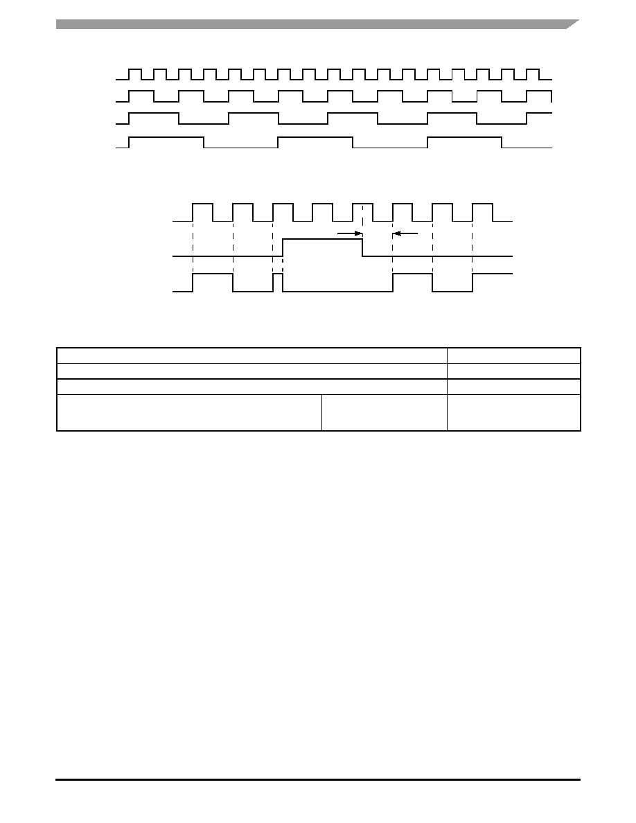
Table 2. Function Tables
CLK
EN
MR
Function
Z
ZZ
X
L
H
X
L
L
H
Divide
Hold Q0:3
Reset Q0:3
X = Don't Care
Z = Low-to-High Transition
ZZ = High-to-Low Transition
DIVSELa
Q0:1 Outputs
L
H
Divide by 2
Divide by 4
DIVSELb
Q2:3 Outputs
L
H
Divide by 4
Divide by 6
Figure 2. Logic Diagram
CLK
CLK
EN
MR
˜2/4
Q0
Q0
Q1
Q1
˜4/6
Q2
Q2
Q3
Q3
R
R
DIVSELa
DIVSELb
V
EE

Advanced Clock Drivers Device Data
4
Freescale Semiconductor
MC100ES6039
Table 4. Maximum Ratings
(1)
1. Maximum Ratings are those values beyond which device damage may occur.
Symbol
Parameter
Condition 1
Condition 2
Rating
Units
V
CC
PECL Mode Power Supply
V
EE
= 0 V
3.9
V
V
EE
ECL Mode Power Supply
V
CC
= 0 V
≠3.9
V
V
I
PECL Mode Input Voltage
ECL Mode Input Voltage
V
EE
= 0 V
V
CC
= 0 V
V
I
V
CC
V
I
V
EE
3.9
≠3.9
V
V
I
out
Output Current
Continuous
Surge
50
100
mA
mA
I
BB
V
BB
Sink/Source
± 0.5
mA
T
A
Operating Temperature Range
≠40 to +85
∞C
T
stg
Storage Temperature Range
≠65 to +150
∞C
JA
Thermal Resistance (Junction-to-Ambient)
0 LFPM
500 LFPM
20 SOIC
20 SOIC
TBD
TBD
∞C/W
∞C/W
Table 5. DC Characteristics (V
CC
= 0 V, V
EE
= ≠3.8 V to ≠3.135 V or V
CC
= 3.135 V to 3.8 V, V
EE
= 0 V)
(1)
1. MC100ES6139 circuits are designed to meet the DC specifications shown in the above table after thermal equilibrium has been established.
The circuit is in a test socket or mounted on a printed circuit board and transverse airflow greater than 500 lfpm is maintained.
Symbol
Characteristic
≠40
∞C
0
∞C to 85∞C
Unit
Min
Typ
Max
Min
Typ
Max
I
EE
Power Supply Current
35
60
35
60
mA
V
OH
Output HIGH Voltage
(2)
2. All loading with 50
to V
CC
≠2.0 volts.
V
CC
≠1150 V
CC
≠1020 V
CC
≠800 V
CC
≠1200 V
CC
≠970
V
CC
≠750
mV
V
OL
Output LOW Voltage
(2)
V
CC
≠1950 V
CC
≠1620 V
CC
≠1250 V
CC
≠2000 V
CC
≠1680 V
CC
≠1300
mV
V
IH
Input HIGH Voltage (Single-Ended)
V
CC
≠1165
V
CC
≠880 V
CC
≠1165
V
CC
≠880
mV
V
IL
Input LOW Voltage (Single-Ended)
V
CC
≠1810
V
CC
≠1475 V
CC
≠1810
V
CC
≠1475
mV
V
BB
Output Reference Voltage
V
CC
≠1400
V
CC
≠1200 V
CC
≠1400
V
CC
≠1200
mV
V
PP
Differential Input Voltage
(3)
3. V
PP
(DC) is the minimum differential input voltage swing required to maintain device functionality.
0.12
1.4
0.12
1.4
V
V
CMR
Differential Cross Point Voltage
(4)
4. V
CMR
(DC) is the crosspoint of the differential input signal. Functional operation is obtained when the crosspoint is within the V
CMR
(DC)
range and the input swing lies within the V
PP
(DC) specification.
V
EE
+0.2
V
CC
≠0.7
V
EE
+0.2
V
CC
≠0.7
V
I
IH
Input HIGH Current
150
150
µA
I
IL
Input LOW Current
0.5
0.5
µA

Advanced Clock Drivers Device Data
Freescale Semiconductor
5
MC100ES6039
Figure 5. Typical Termination for Output Driver and Device Evaluation
Table 6. AC Characteristics (V
CC
= 0 V, V
EE
= ≠3.8 V to ≠3.135 V or V
CC
= 3.135 V to 3.8 V, V
EE
= 0 V)
(1)
1. Measured using a 750 mV source, 50% duty cycle clock source. All loading with 50
to V
CC
≠2.0 V.
Symbol
Characteristic
≠40
∞C
25
∞C
85
∞C
Unit
Min
Typ
Max
Min
Typ
Max
Min
Typ
Max
f
max
Maximum Frequency
> 1
> 1
> 1
GHz
t
PLH
,
t
PHL
Propagation Delay
CLK, Q (Diff)
MR, Q
575
500
875
850
575
500
875
850
575
500
875
850
ps
ps
t
RR
Reset Recovery
200
100
200
100
200
100
ps
t
s
Setup Time
EN, CLK
DIVSEL, CLK
200
400
120
180
200
400
120
180
200
400
120
180
ps
ps
t
h
Hold Time
CLK, EN
CLK, DIVSEL
100
200
50
140
100
200
50
140
100
200
50
140
ps
ps
t
PW
Minimum Pulse Width
MR
550
450
550
450
550
450
ps
t
SKEW
Within Device Skew
Q, Q
Q, Q @ Same Frequency
Device-to-Device Skew
(2)
2. Skew is measured between outputs under identical transitions. Duty cycle skew is defined only for differential operation when the delays are
measured from the cross point of the inputs to the cross point of the outputs.
80
50
300
80
50
300
80
50
300
ps
ps
ps
t
JITTER
Cycle-to-Cycle Jitter
(RMS 1
)
1
1
1
ps
V
PP
Input Voltage Swing (Differential)
150
1400
150
1400
150
1400
mV
V
CMR
Differential Cross Point Voltage
V
EE
+0.2
V
CC
≠1.1 V
EE
+0.2
V
CC
≠1.1 V
EE
+0.2
V
CC
≠1.1
V
t
r
t
f
Output Rise/Fall Times
Q, Q
(20% ≠ 80%)
50
300
50
300
50
300
ps
Driver
Device
Receiver
Device
Q
D
50
Q
D
50
V
TT
V
TT
= V
CC
≠- 2.0 V