 | –≠–ª–µ–∫—Ç—Ä–æ–Ω–Ω—ã–π –∫–æ–º–ø–æ–Ω–µ–Ω—Ç: MC145017 | –°–∫–∞—á–∞—Ç—å:  PDF PDF  ZIP ZIP |
MC145017
Rev 5, 05/2005
Freescale Semiconductor
Technical Data
© Freescale Semiconductor, Inc., 2005. All rights reserved.
Low-Power CMOS
Ionization Smoke Detector IC
with Temporal Pattern Horn Driver
The MC145017, when used with an ionization chamber and a small number
of external components, will detect smoke. When smoke is sensed, an alarm is
sounded via an external piezoelectric transducer and internal drivers. This circuit
is designed to operate in smoke detector systems that comply with UL217 and
UL268 specifications.
Features
∑
Ionization Type with On-Chip FET Input Comparator
∑
Piezoelectric Horn Driver
∑
Guard Outputs on Both Sides of Detect Input
∑
Input-Production Diodes on the Detect Input
∑
Low-Battery Trip Point, Internally Set, can be Altered Via External Resistor
∑
Detect Threshold, Internally Set, can be Altered Via External Resistor
∑
Pulse Testing for Low Battery Uses LED for Battery Loading
∑
Comparator Outputs for Detect and Low Battery
∑
Internal Reverse Battery Protection
∑
Supports NFPA 72, ANSi 53.41, and ISO 8201 Audible Emergency
Evacuation Signals
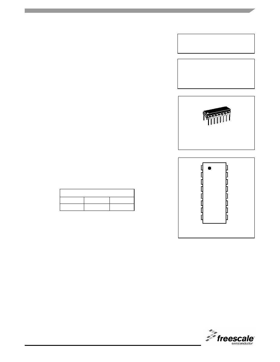
ORDERING INFORMATION
Device
Case No.
Package
MC145017P
648-08
Plastic Dip
MC145017
P SUFFIX
PLASTIC DIP
CASE 648-08
LOW-POWER CMOS IONIZATION
SMOKE DETECTOR IC WITH
TEMPORAL PATTERN
HORN DRIVER
Figure 1. . Pin Connections
16
15
14
13
12
11
10
9
1
2
3
4
5
6
7
8
Detect
Comp. Out
N/C
Low V Set
Low V
Comp. Out
LED
V
DD
Timing
Resistor
Feedback
Guard Hi-Z
Detect Input
Guard Lo-Z
Sensitivity Set
Osc Capacitor
Silver
Brass
V
SS
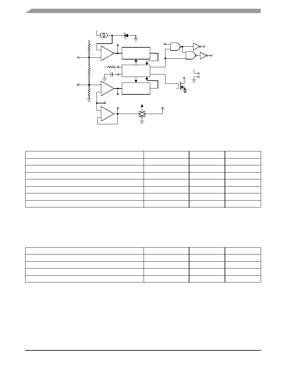
Sensors
2
Freescale Semiconductor
MC145017
Figure 2. Block Diagram
This device contains circuitry to protect the inputs against damage due to high static voltages or electric fields; however, it is advised that
normal precautions be taken to avoid application of any voltage higher than maximum rated voltages to this high impedance circuit. For
proper operation it is recommended that V
in
and V
out
be constrained to the range V
SS
(V
in
or V
out
)
V
DD
.
Table 1. Maximum Ratings
(1)
(Voltages referenced to V
SS
)
1. Maximum Ratings are those values beyond which damage to the device may occur.
Rating
Symbol
Value
Unit
DC Supply Voltage
V
DD
-0.5 to + 15
V
Input Voltage, All Inputs Except Pin 8
V
in
-0.25 to V
DD
+0.25
V
DC Current Drain per Input Pin, Except Pin 15 = 1 mA
I
10
mA
DC Current Drain per Output Pin
I
30
mA
Operating Temperature Range
T
A
-10 to +60
∞C
Storage Temperature Range
T
stg
-55 to +125
∞C
Reverse Battery Time
t
RB
5.0
s
Table 2. Recommended Operating Conditions
(Voltages referenced to V
SS
)
Parameter
Symbol
Value
Unit
Supply Voltage
V
DD
9.0
V
Timing Capacitor
--
0.1
µF
Timing Resistor
--
8.2
M
Battery Load (Resistor or LED)
--
10
mA
3
+
-
V
DD
Latch
Low Battery Comp.
Oscillator
Latch
+
-
V
DD
80 K
1045 K
7
12
1
13
1125 K
+
-
15
Detect Input
14
Lo-Z
Active
Guard
16
HI-Z
V
DD
4
V
DD
8
Piezoelectric
Horn Driver
11
10
5
LED Driver
V
DD
6
9
Sensors
Freescale Semiconductor
3
MC145017
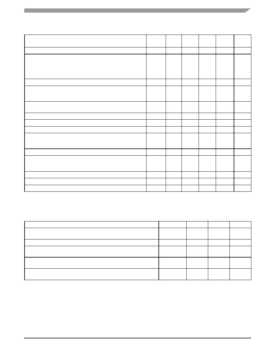
Table 3. Electrical Characteristics
(1)
(Voltages referenced to V
SS
, T
A
= 25
∞C)
1. Data labelled "Typ" is not to be used for design purposes but is intended as an indication of the IC's potential performance.
Characteristic
Symbol
V
DD
V
DC
Min
Typ
Max
Unit
Operating Voltage
V
DD
--
6.0
--
12
V
Output Voltage
Piezoelectric Horn Drivers (I
OH
= -16 mA)
Comparators (I
OH
= -30
µA)
Piezoelectric Horn Drivers (I
OL
= +16 mA)
Comparators (I
OL
= +30
µA)
V
OH
V
OL
7.2
9.0
7.2
9.0
6.3
8.5
--
--
--
8.8
--
0.1
--
--
0.9
0.5
V
V
Output Voltage -- LED Driver, I
OL
= 10 mA
V
OL
7.2
--
--
3.0
V
Output Impedance, Active Guard
Pin 14
Pin 16
Lo-Z
Hi-Z
9.0
9.0
--
--
--
--
10
1000
k
Operating Current (R
bias
= 8.2 M
)
I
DD
9.0
12.0
--
--
3.2
--
7.0
10.0
µA
Input Current -- Detect (40% R.H.)
I
in
9.0
--
--
±1.0
pA
Input Current, Pin 8
I
in
9.0
--
--
±0.1
µA
Input Current @ 50
∞C, Pin 15
I
in
--
--
--
±6.0
pA
Internal Set Voltage
Low Battery
Sensitivity
V
low
V
set
9.0
--
7.2
47
--
50
7.8
53
V
%V
DD
Hysteresis
v
hys
9.0
75
100
150
mV
Offset Voltage (measured at V
in
= V
DD
/2
Active Guard
Detect Comparator
V
OS
9.0
9.0
--
--
--
--
±100
±50
mV
Input Voltage Range, Pin 8
V
in
--
V
SS
-10
--
V
DD
+ 10
V
Input Capacitance
C
in
--
--
5.0
--
pF
Common Mode Voltage Range, Pin 15
V
cm
--
0.6
--
V
DD
- 2
V
Table 4. Timing Parameters
(C = 0.1
µF, R
bias
= 8.2 M
, V
DD
= 9.0 V, T
A
= 25∞C, See
Figure 7
)
Characteristics
Symbol
Min
Max
Units
Oscillator Period
No Smoke
Smoke
t
CI
1.46
37.5
1.85
45.8
s
ms
Oscillator Rise Time
t
r
10.1
12.3
ms
Horn Output
On Time
(During Smoke)
Off Time
PW
on
PW
off
450
450
550
550
ms
ms
LED Output
Between Pulses
On Time
t
LED
PW
on
35.0
10.1
44.5
12.3
s
ms
Horn Output
On Time
(During Low Battery)
Between Pulses
t
on
t
off
10.1
35.0
12.3
44.5
ms
s
Sensors
4
Freescale Semiconductor
MC145017
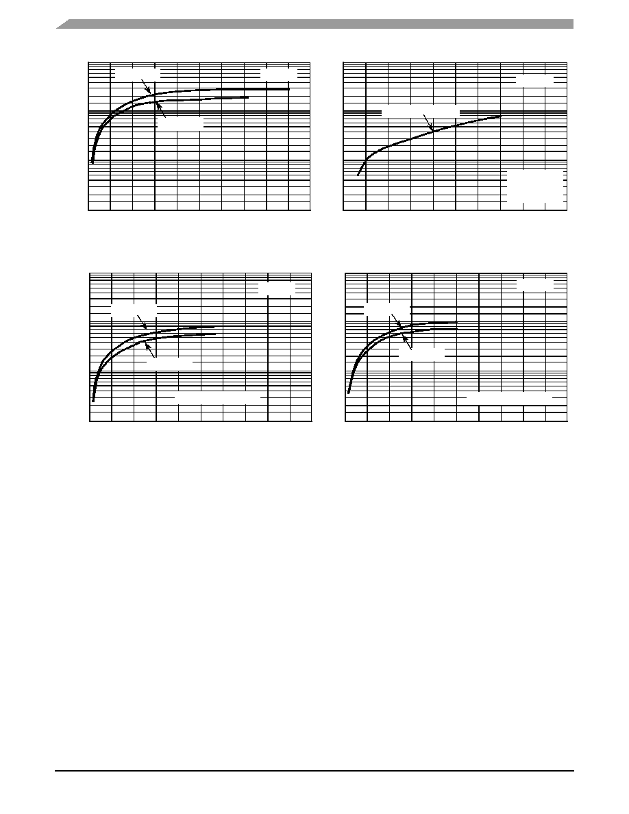
Figure 3. Typical LED Output I≠V Characteristic
Figure 4. Typical Comparator Output I≠V Characteristic
Figure 5. Typical P Horn Driver Output I≠V Characteristic
DEVICE OPERATION
Timing
The internal oscillator of the MC145017 operates with a
period of 1.65 seconds during no-smoke conditions. Each
1.65 seconds, internal power is applied to the entire IC and a
check is made for smoke, except during LED pulse, Low
Battery Alarm Chirp, or Horn Modulation (in smoke). Every 24
clock cycles a check is made for low battery by comparing
V
DD
to an internal zener voltage. Since very small currents
are used in the oscillator, the oscillator capacitor should be of
a low leakage type.
Detect Circuitry
If smoke is detected, the oscillator period becomes
41.67 ms and the piezoelectric horn oscillator circuit is
enabled. The horn output is modulated 500 ms on, 500 ms
off. During the off time, smoke is again checked and will
inhibit further horn output if no smoke is sensed. During
smoke conditions the low battery alarm is inhibited, but the
LED pulses at a 1.0 Hz rate.
An active guard is provided on both pins adjacent to the
detect input. The voltage at these pins will be within 100 mV
of the input signal. This will keep surface leakage currents to
a minimum and provide a method of measuring the input
voltage without loading the ionization chamber. The active
guard op amp is not power strobed and thus gives constant
protection from surface leakage currents. Pin 15 (the Detect
input) has internal diode protection against static damage.
Sensitivity/Low Battery Thresholds
Both the sensitivity threshold and the low battery voltage
levels are set internally by a common voltage divider (please
see
Figure 2
) connected between V
DD
and V
SS
. These
voltages can be altered by external resistors connected from
pins 3 or 13 to either V
DD
or V
SS
. There will be a slight
interaction here due to the common voltage divider network.
The sensitivity threshold can also be set by adjusting the
smoke chamber ionization source.
Test Mode
Since the internal op amps and comparators are power
strobed, adjustments for sensitivity or low battery level could
be difficult and/or time-consuming. By forcing Pin 12 to V
SS
,
the power strobing is bypassed and the outputs, Pins 1 and
4, constantly show smoke/no smoke and good battery/low
0
1
2
3
4
5
6
7
8
9
10
0.1
1.0
10.0
100.0
V
DS
, Drain To Source Voltage (Vdc)
I
D
,
D
r
ai
n C
u
rre
n
t
(m
A
)
0
1
2
3
4
5
6
7
8
9
10
0.01
0.1
1.0
10.0
V
DS
, Drain To Source Voltage (Vdc)
I
D
, Drain Curren
t (mA)
V
DD
= 9.0 Vdc
V
DD
= 7.2 Vdc
T
A
= 25
∞C
V
DD
= 9.0 Vdc or 7.2 Vdc
T
A
= 25
∞C
P-CH Source
And N-CH Sink
Current
0
1
2
3
4
5
6
7
8
9
10
1.0
10.0
100.0
1000.0
I
D
, Drain
Cu
rrent
(mA)
V
DS
, Drain To Source Voltage (Vdc)
V
DD
= 9.0 Vdc
T
A
= 25
∞C
V
DD
= 7.2 Vdc
P-CH Source Current
0
1
2
3
4
5
6
7
8
9
10
1.0
10.0
100.0
1000.0
V
DS
, Drain To Source Voltage (Vdc)
I
D
,
Drain Curre
n
t (mA)
V
DD
= 9.0 Vdc
V
DD
= 7.2 Vdc
T
A
= 25
∞C
N-CH Sink Current
Sensors
Freescale Semiconductor
5
MC145017
battery, respectively. Pin 1 = V
DD
for smoke and Pin 4 = V
DD
for low battery. In this mode and during the 10 ms power
strobe, chip current rises to approximately 50
µA.
Led Pulse
The 9-volt battery level is checked every 40 seconds
during the LED pulse. The battery is loaded via a 10 mA
pulse for 11.6 ms. If the LED is not used, it should be
replaced with an equivalent resistor such that the battery
loading remains at 10 mA.
Hysteresis
When smoke is detected, the resistor/divider network that
sets sensitivity is altered to increase sensitivity. This yields
approximately 100 mV of hysteresis and reduces false
triggering.
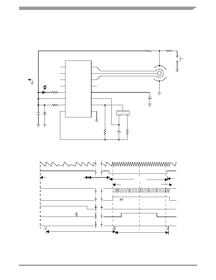
Figure 6. Typical Application as Ionization Smoke Detector
Figure 7. MC145017 Timing Diagram
MC145017
1
16
2
3
4
5
6
7
8
15
14
13
12
11
10
9
330
8.2 M
+
9 V
0.1
µF
1.5 M
*
0.001
µF
220 k
*
0.1
µF
1 M
1 M
Test
*NOTE: Component values may change depending on type of piezoelectric horn used.
OSC
Pin 12
Smoke - N
- Y
Low Bat - Y
- N
HYST
Pin 13
Horn - On
- Off
LED - Off
- On
2
3
4
5
6
7
9
8
1
No Smk
No Low Bat
LOW BATTERY CHIRP
OSC
Pin 12
Smoke - N
- Y
No Smk
23
24 1
6
12
18
24
Smoke
Latch Alarm Condition
( 100 mV Level Shift)
NFPA MOD
LOW BAT - Y
- N
HORN - ON
- OFF
LED - OFF
- ON
(Note 1)
24 Clocks
24 Clocks
No Smoke, Low Battery
>>
>>
> >
NOTES:
1. Horn modulation is self-completing. When going from smoke to no smoke, the alarm condition will terminate only when horn is off.
2. Comparators are strobed once per cycle (1.65 sec for no smoke, 40 msec for smoke).
Sensors
6
Freescale Semiconductor
MC145017
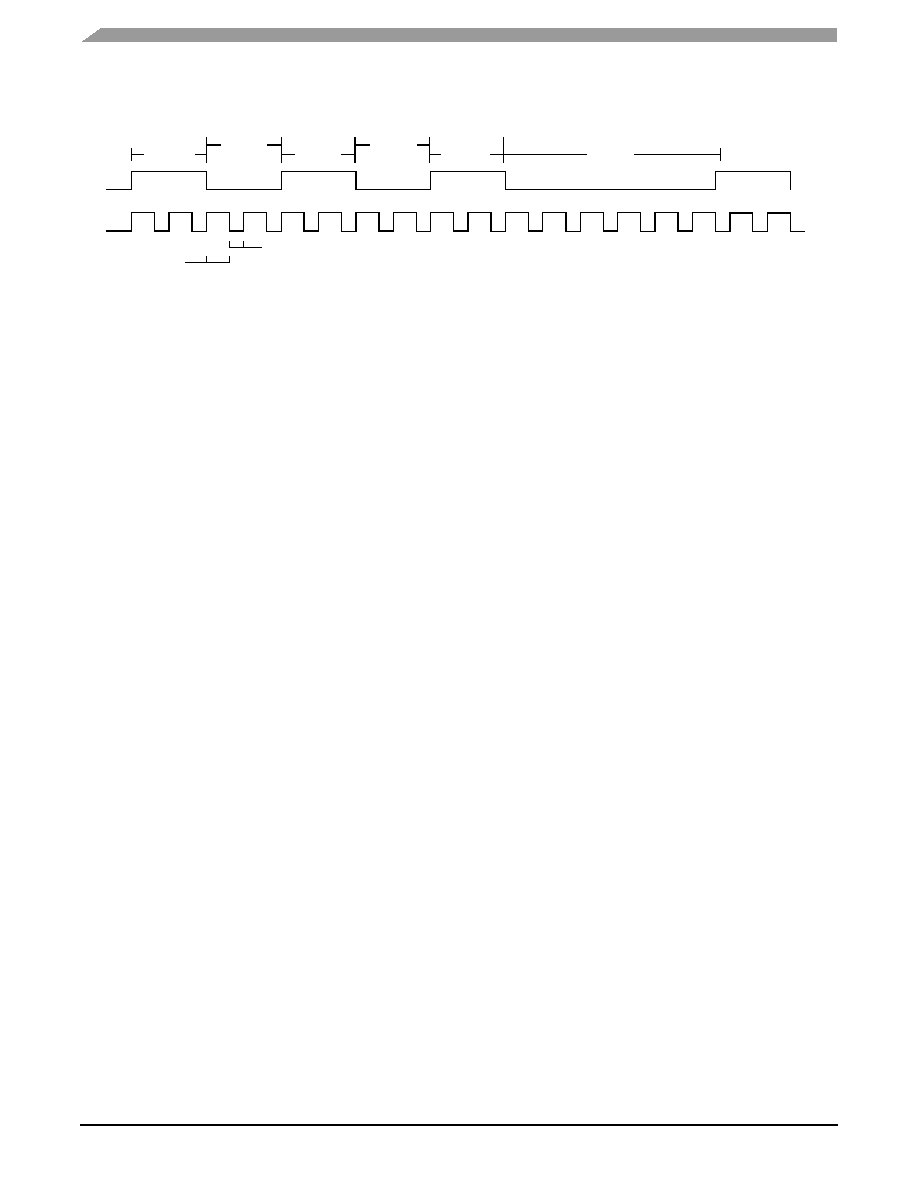
Figure 8. Horn Modulation
NFPA72: Temporal Horn
Modulation Pattern
Traditional 4/6 Horn
Modulation Pattern
0.5 Sec
0.5 Sec
0.5 Sec
0.5 Sec
0.5 Sec
1.5 Sec
167 Msec
83 Msec

Sensors
Freescale Semiconductor
7
MC145017
PACKAGE DIMENSIONS
NOTES:
1.
2.
3.
4.
5.
DIMENSIONING AND TOLERANCING PER ANSI
Y14.5M, 1982.
CONTROLLING DIMENSION: INCH.
DIMENSION L TO CENTER OF LEADS WHEN
FORMED PARALLEL.
DIMENSION B DOES NOT INCLUDE MOLD FLASH.
ROUNDED CORNERS OPTIONAL.
-A-
B
F
C
S
H
G
D
16 PL
J
L
M
SEATING
PLANE
1
8
9
16
K
-T-
M
A
M
0.25 (0.010)
T
DIM
MIN
MAX
MIN
MAX
MILLIMETERS
INCHES
A
0.740
0.770
18.80
19.55
B
0.250
0.270
6.35
6.85
C
0.145
0.175
3.69
4.44
D
0.015
0.021
0.39
0.53
F
0.040
0.70
1.02
1.77
G
0.100 BSC
2.54 BSC
H
0.050 BSC
1.27 BSC
J
0.008
0.015
0.21
0.38
K
0.110
0.130
2.80
3.30
L
0.295
0.305
7.50
7.74
M
0
10
0
10
S
0.020
0.040
0.51
1.01
STYLE 1:
PIN 1. CATHODE
2. CATHODE
3. CATHODE
4. CATHODE
5. CATHODE
6. CATHODE
7. CATHODE
8. CATHODE
9. ANODE
10. ANODE
11. ANODE
12. ANODE
13. ANODE
14. ANODE
15. ANODE
16. ANODE
STYLE 2:
PIN 1. COMMON DRAIN
2. COMMON DRAIN
3. COMMON DRAIN
4. COMMON DRAIN
5. COMMON DRAIN
6. COMMON DRAIN
7. COMMON DRAIN
8. COMMON DRAIN
9. GATE
10. SOURCE
11. GATE
12. SOURCE
13. GATE
14. SOURCE
15. GATE
16. SOURCE
CASE 648-08
ISSUE R
16-LEAD PLASTIC DIP

How to Reach Us:
Home Page:
www.freescale.com
E-mail:
support@freescale.com
USA/Europe or Locations Not Listed:
Freescale Semiconductor
Technical Information Center, CH370
1300 N. Alma School Road
Chandler, Arizona 85224
+1-800-521-6274 or +1-480-768-2130
support@freescale.com
Europe, Middle East, and Africa:
Freescale Halbleiter Deutschland GmbH
Technical Information Center
Schatzbogen 7
81829 Muenchen, Germany
+44 1296 380 456 (English)
+46 8 52200080 (English)
+49 89 92103 559 (German)
+33 1 69 35 48 48 (French)
support@freescale.com
Japan:
Freescale Semiconductor Japan Ltd.
Headquarters
ARCO Tower 15F
1-8-1, Shimo-Meguro, Meguro-ku,
Tokyo 153-0064
Japan
0120 191014 or +81 3 5437 9125
support.japan@freescale.com
Asia/Pacific:
Freescale Semiconductor Hong Kong Ltd.
Technical Information Center
2 Dai King Street
Tai Po Industrial Estate
Tai Po, N.T., Hong Kong
+800 2666 8080
support.asia@freescale.com
For Literature Requests Only:
Freescale Semiconductor Literature Distribution Center
P.O. Box 5405
Denver, Colorado 80217
1-800-441-2447 or 303-675-2140
Fax: 303-675-2150
LDCForFreescaleSemiconductor@hibbertgroup.com
MC145017
Rev. 5
05/2005
Information in this document is provided solely to enable system and software
implementers to use Freescale Semiconductor products. There are no express or
implied copyright licenses granted hereunder to design or fabricate any integrated
circuits or integrated circuits based on the information in this document.
Freescale Semiconductor reserves the right to make changes without further notice to
any products herein. Freescale Semiconductor makes no warranty, representation or
guarantee regarding the suitability of its products for any particular purpose, nor does
Freescale Semiconductor assume any liability arising out of the application or use of any
product or circuit, and specifically disclaims any and all liability, including without
limitation consequential or incidental damages. "Typical" parameters that may be
provided in Freescale Semiconductor data sheets and/or specifications can and do vary
in different applications and actual performance may vary over time. All operating
parameters, including "Typicals", must be validated for each customer application by
customer's technical experts. Freescale Semiconductor does not convey any license
under its patent rights nor the rights of others. Freescale Semiconductor products are
not designed, intended, or authorized for use as components in systems intended for
surgical implant into the body, or other applications intended to support or sustain life,
or for any other application in which the failure of the Freescale Semiconductor product
could create a situation where personal injury or death may occur. Should Buyer
purchase or use Freescale Semiconductor products for any such unintended or
unauthorized application, Buyer shall indemnify and hold Freescale Semiconductor and
its officers, employees, subsidiaries, affiliates, and distributors harmless against all
claims, costs, damages, and expenses, and reasonable attorney fees arising out of,
directly or indirectly, any claim of personal injury or death associated with such
unintended or unauthorized use, even if such claim alleges that Freescale
Semiconductor was negligent regarding the design or manufacture of the part.
FreescaleTM and the Freescale logo are trademarks of Freescale Semiconductor, Inc.
All other product or service names are the property of their respective owners.
© Freescale Semiconductor, Inc. 2005. All rights reserved.