 | –≠–ª–µ–∫—Ç—Ä–æ–Ω–Ω—ã–π –∫–æ–º–ø–æ–Ω–µ–Ω—Ç: MC33285D | –°–∫–∞—á–∞—Ç—å:  PDF PDF  ZIP ZIP |
©
Motorola,Inc 1999
Rev 2.4
MOTOROLA
SEMICONDUCTOR
TECHNICAL DATA
This document contains information on a new product under development. Motorola reserves the
right to change or discontinue this product without notice.
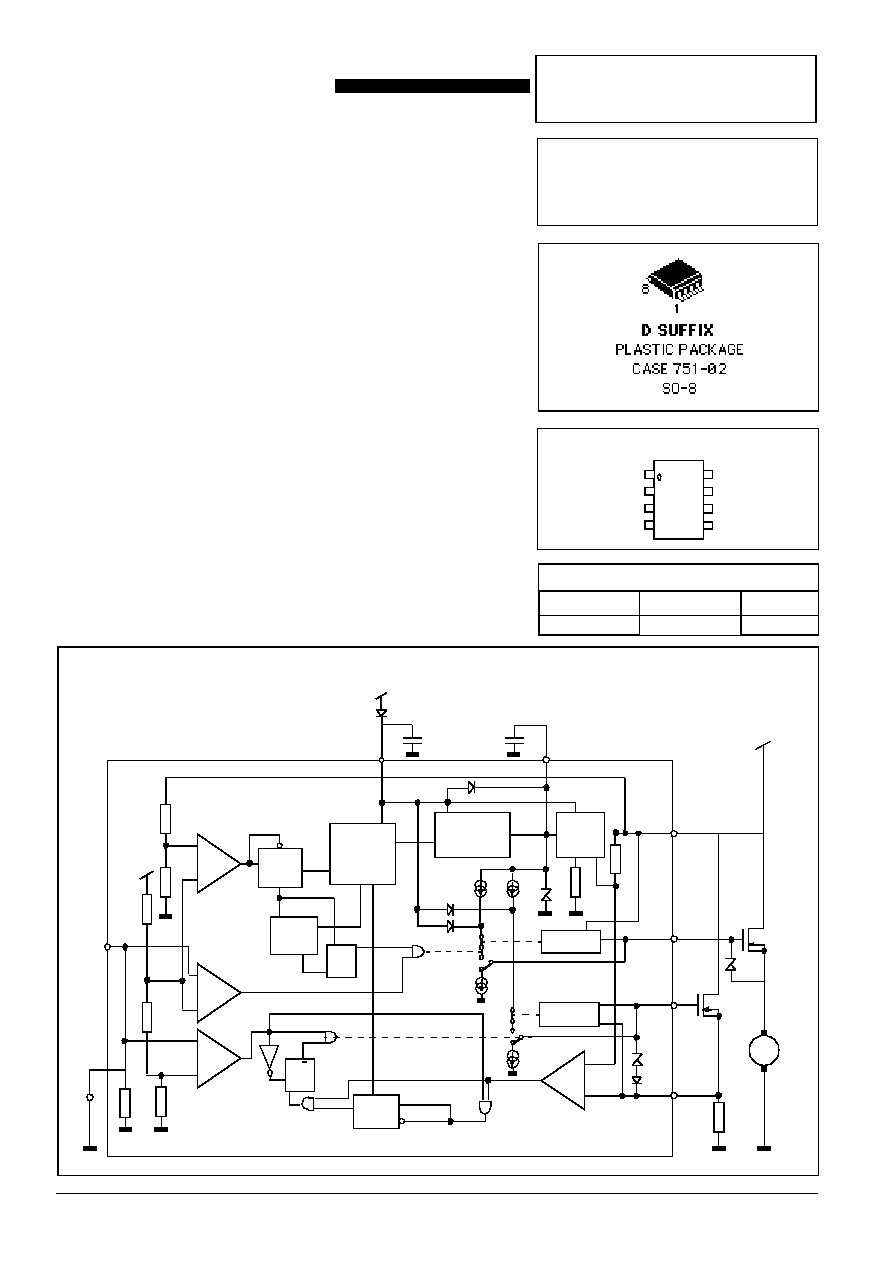
PIN CONNECTIONS
MC33285
Product Preview
HIGH SIDE
TMOS DRIVER
Block Diagram And Typical Application
SRC
OUT1
DRN
OUT2
1
2
3
5
4
6
7
8
IN
GND
V
CC
CP
GND
I
OUTN2
OUT2
OUT1
SRC
IN
VCC
Band-
Rthr
DRN
I
OUTN1
V
OUT2
-V
DRN
> V
TH2
V
OUT1
-V
SRC
> V
TH1
I
ON2
I
ON1
gap
CP
Charge
pump
Oscillator
and
Divider
t
LDdet
R
S
t
OUT2ect
Load Dump
R
S
Q
Detection
t
OCdet
S
R Q
start t
OCdet
OCPC
OUT2 Activation
Time
THRIN1
THRIN2
V
REF
C
CP
V
IGN
M
Kl.30
OC Detection
+
-
-
+
+
-
+
-
Automotive Dual High
Side TMOS Driver
ORDERING INFORMATION
Device
Temperature
Range
Package
SO8
-40
∞
C to +125
∞
C
MC33285D
SILICON MONOLITHIC
INTEGRATED CIRCUIT
The MC33285 is a dual high side TMOS driver designed for use in
the harsh automotive switching applications.
The purpose of the MC33285 is to drive two power n-channel FETs in
a high side application with an inductive load. The application in an
automotive environment requires the capability of withstanding high
voltages and load dump transients. The MC33285 is able to withstand
reverse battery conditions at selected pins.
It protects the n-channel power FET on OUT1 under over current
condition. This device has one input to control both stages on or off.
∑ Temperature Range from -40
∞
C to +125
∞
C
∑ PWM Capability
∑ Power TMOS # 1 Over-Current and Short-Circuit Protection
∑ Voltage Range 7V to 40V
∑ Extended Temperature Range from -40
∞
C to 125
∞
C
∑ Load Dump Protected
∑ Over Voltage Detection and Activation of OUT2 during Overvoltage
∑ Single Input Control for both Output Stages
∑ Capacitor Value of 100nF Connected to Pin CP
∑ Analog Input Control Measurement Detection
∑ OUT1 LOAD leakage measurement detection
F
r
e
e
s
c
a
l
e
S
e
m
i
c
o
n
d
u
c
t
o
r
,
I
Freescale Semiconductor, Inc.
For More Information On This Product,
Go to: www.freescale.com
n
c
.
.
.
MC33285
MOTOROLA
2
MC33285
MAXIMUM RATING
THERMAL RATINGS
ELECTRICAL CHARACTERISTICS.
(T
A
from -40
∞
C to +125
∞
C, Vcc from 7V to 20V, unless otherwise noted)
SRC PIN 1
DRN PIN 3
OUT1 PIN2, OUT 2 PIN 4
VCC PIN 6
IN PIN 8
Rating
Symbol
Value
Unit
Maximum voltage at pins OUT1 OUT2
V
OUT
V
VCC
+ 20
V
Maximum voltage at pin CP
V
CP
50
V
Input voltage V
i
at DRN
V
DRN
-2 ; 40
V
Input voltage V
i
at SRC
V
SRC
-5 ; 40
V
Input voltage at pin V
CC
V
CC
-2 to 40
V
Input Voltage at pin IN. Condition : -2V<V
VCC
<40V
V
IN
-2 to V
VCC
V
Operational voltage V
VCC
at pin V
CC
V
VCC
7 to V
i
V
Rating
Symbol
Value
Unit
Storage Temperature
T
stg
-40 to +150
∞
C
Operating ambient temperature
T
a
-40 to +125
∞
C
Characteristic
Symbol
Min
Typ
Max
Unit
OVERVOLTAGE AND OVERCURRENT
Load Dump Detection Time
tLD
det
250
400
550
µ
s
Load Dump Activation Time
tOUT2act
300
460
620
ms
Error Voltage Threshold
VDRN - VSRC
1.12
1.44
V
Overcurrent Detection Time
tOCdet
520
800
1080
µ
s
Leakage Current
ILC
det
15
30
50
mA
Leakage Current Detection Time
tLC
det
130
200
270
µ
s
Operating Current (7V<V
DRN
<20V)
I
DRN
1.5
mA
Leakage current (0V<V
DRN
<20V, V
VCC
<4V)
I
leak_DRN
-5
5
µ
A
Output On Voltage. Charge Pump ON
Von
Vcc+15
V
Turn off current, Vout >0.5V
Ioutoff
66
110
154
µ
A
Turn On Time, OUT1: 8nF,10
µ ;
OUT2:
16nF,10
µ
- 7V < Vcc < 10V, Vout > Vcc+7
- 10V < Vcc < 20V, Vout > Vcc+11
ton
1.5
1.5
ms
Supply Voltage Range
Vcc
7
40
V
Quiescent Supply Current at Vcc = 20V
Icc
10
mA
Input Low Voltage OUT1
Vil
0.7
V
Input High Voltage OUT1
Vih
1.7
V
Input Hysteresis OUT1, OUT2
Vhys
0.4
V
Input Pull Down Current, 0.7V<Vin<6V
Iin
7.5
15
16.5
µ
A
Open Input Voltage
Viop
0.7
V
Input Low Voltage OUT2
Vil2
3
V
Input High Voltage OUT2
Vih2
3.9
V
F
r
e
e
s
c
a
l
e
S
e
m
i
c
o
n
d
u
c
t
o
r
,
I
Freescale Semiconductor, Inc.
For More Information On This Product,
Go to: www.freescale.com
n
c
.
.
.
MC33285
MOTOROLA
3
MC33285
Turn On Characteristics
The power FETs are turned on by charging their gate capacities with a current flowing out of pin OUT1 and OUT2.
During PWM, the values of table below are guaranteed. They are measured with 8nF on OUT1 and 16nF on OUT2.
- test condition : V
IN
: ramp 0V to 2.5V or 2.5V to 5V.
Figure 1.
Turn-on Behaviour
Table 1 Turn on behaviour
The output voltages at OUT1 and OUT2 are limited by controlling the current sources I
on1
, I
on2
to avoid currrent flowing
through the external or the internal zener diode .
If Vcc + Vth (threshold voltage) is reached , the current sources are turned off.
- threshold V
TH1
for OUT1 output voltage control : 7V < V
TH1
< Vz
- threshold VTH2 for OUT2 output voltage control : 7V < V
TH2
< 15V
Turn off characteristics
The power FETs on OUT1 and OUT2 are turned off by discharging the gate capacity with the constant discharge current
I
OUToff
.
- discharge current I
OUTxoff
: IOUTxoff = 110
µ
A
condition : V
OUT
x > 0.5V ( V
IN
< V
THRxIN
)
Test conditions for switching off the power FETs :
- 1. IN open
- 2. Stages disabled via pin IN
- 3. Stage OUT1 disabled by an over current error
Voltage V
VCC
Minimum V
OUT1,OUT2
after t
on1
= 100
µ
sec
Minimum V
OUT1,OUT2
after t
on2
= 1.0msec
Minimum V
OUT1,OUT2
after t
on3
= 1.5msec
7V < V
VCC
< 10V
10V < V
VCC
< 20V
20V < V
VCC
< 40V
V
VCC
- 0.7V
V
VCC
- 0.7V
V
VCC
- 0.7V
V
VCC
+ 5.95V
V
VCC
+ 9.35V
V
VCC
+ 7V
V
VCC
+ 11V
20ms
V
OUT2
2.5V
5V
IN
V
CCP
T H R I N 1
THRIN2
IN
V
OUT1
V
OUT2
0V
0V
2.5V
V
OUT1
IN
VOUT1
max
ton1
ton2
ton3
0
2.5V
0V
5V
V
OUT2
IN
VOUT2
max
ton1
ton2
ton3
0
V
VCC
+7V
F
r
e
e
s
c
a
l
e
S
e
m
i
c
o
n
d
u
c
t
o
r
,
I
Freescale Semiconductor, Inc.
For More Information On This Product,
Go to: www.freescale.com
n
c
.
.
.

MC33285
MOTOROLA
4
MC33285
FUNCTIONNAL DESCRIPTION
Introduction
The MC33285 contains only one charge pump for two
outputs.The outputs OUT1 and OUT2 are switched on and off
by the input IN .There are three ways to control the outputs:
OUt1 can be switched alone , they can be switched together
or OUT2 can be switched when OUT1 is already on .In the last
case , the voltage drop on OUT1 when charging OUT2 is
limited .
The external capacitor C
CP
connected to pin CP is used to
store the charge continuously delivered by the charge pump .
The voltage on this pin is limited to a maximum value V
CPmax
.
Both outputs are sourced with a constant current from C
CP
to
switch them on . In addition , the gates of the power FETs are
precharged from VCC to prevent C
CP
from being discharged
by a voltage on OUT1 or OUT2 which is still lower than
V
VCC
.The values of the output voltages are limited to
V
OUT1max
and V
OUT2max
The power FET on OUT1 is protected againts an
exceeded gate-source voltage by an internal zener diode.
Channel 1 allows to protect the n-channel power FET on
OUT1 under over current condition. The drain-source voltage
of the FET on OUT1 will be checked, if the channel 1 is
switched on. The internal error voltage threshold determines
the maximum drain-source voltage that allows the power FET
to stay in the on state. If the measured drain-source voltage
exceeds the internal error voltage threshold, the output of the
Over Current Protection Comparator (OCPC) is enabled. If
the output of the OCPC is active longer than t
OCdet
, the output
OUT1 is switched off .
After switching off the power FET on OUT1 by an over
current condition, the power FET can only be turned on again
by the input IN.
When switching off the power FETs their gate capacities
are discharged by a constant currennt I
OUToff
IF the input IN is disconnected, the MC33285 outputs
OUT1 and OUT2 are in the off state.
If overvoltage occurs on pin DRN for a time period longer
than t
LDdet
, then OUT2 is switched on for the time t
OUT2act
. In
overvoltage condition OUT1 is off if IN is below Vih.
Internal Zener Diode
An on-chip zener diode is placed between OUT1 and
SRC. Design guarantees that V
Z
> V
TH1
- zener clamping voltage between OUT1 and SRC :
V
TH1
< V
Z
< 20V
PWM capability
The CPIC2 is PWM capable on OUT2. The loss of charge
on Ccp when switching on OUT2 is refreshed until the start on
the next PWM cycle to a value which is sufficient to guarantee
the specified turn on behaviour.
The PWM capability is measured with a test circuit and
load conditions
- PWM cycle : period T = 20ms ; OUT2 is switched on from
10% to 90% of T .
- Test condition : V
IN
: ramps 2.5V to 5V according to PWM
cycle defined above.
Crosstalk between OUT1 and OUT2
If output OUT2 is switched on while OUT1 is already on,
the voltage drop that occurs on OUT1 is limited.
Voltage drop on OUT1 :
10V < V
VCC
< 20V : OUT1 not below V
VCC
+ 7V
7V < V
VCC
< 20V : OUT1 not below V
VCC
+ 7V
Each time OUT1 is switched on, a current ILCdet is
sourced out of pin SRC for the time tLCdet to check if there is
an external leakage current on that node in the application.
The high side switch on OUT1 is turned on only if the test is
successful."
F
r
e
e
s
c
a
l
e
S
e
m
i
c
o
n
d
u
c
t
o
r
,
I
Freescale Semiconductor, Inc.
For More Information On This Product,
Go to: www.freescale.com
n
c
.
.
.
MC33285
MOTOROLA
5
MC33285
Motorola reserves the right to make changes without further notice to any products herein to improve
reliability, function or design. Motorola does not assume any liability arising out of the application or use of any
product or circuit described herein ; neither does it convert any licence under its patent rights of others. Motorola
products are not authorized for use as components in life support devices or systems intended for surgical implant
into the body or intended to support or sustain life. Buyer agrees to notify Motorola of any such intended end use
whereupon Motorola shall determine availability and suitability of its products for the use intended. Motorola and
are registered trademarks of Motorola, Inc. Motorola, Inc. is an Equal Employment opportunity/Affirmative
Action Employer.
F
r
e
e
s
c
a
l
e
S
e
m
i
c
o
n
d
u
c
t
o
r
,
I
Freescale Semiconductor, Inc.
For More Information On This Product,
Go to: www.freescale.com
n
c
.
.
.