 | –≠–ª–µ–∫—Ç—Ä–æ–Ω–Ω—ã–π –∫–æ–º–ø–æ–Ω–µ–Ω—Ç: MC34652 | –°–∫–∞—á–∞—Ç—å:  PDF PDF  ZIP ZIP |
Document order number:
MC34652
Rev 6.0, 02/2006
Freescale Semiconductor
Technical Data
* This document contains certain information on a new product.
Specifications and information herein are subject to change without notice.
© Freescale Semiconductor, Inc., 2006. All rights reserved.
2.0 A Negative Voltage Hot
Swap Controller with Enhanced
Programmability
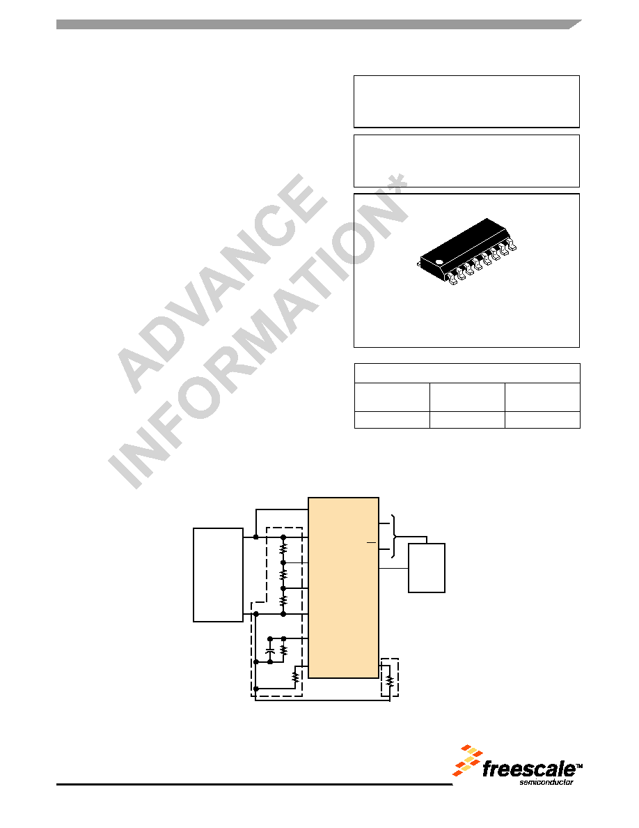
The 34652 is a highly integrated -48 V hot swap controller with an
internal Power MOSFET. It provides the means to safely install and
remove boards from live -48 V backplanes without having to power
down the entire system. It regulates the inrush current, from the
supply to the load's filter capacitor, to a user-programmable limit,
allowing the system to safely stabilize. A disable function allows the
user to disable the 34652 manually or through a microprocessor and
safely disconnect the load from the main power line.
The 34652 has active high and active low power good output
signals that can be used to directly enable a power module load.
Programmable under- and overvoltage detection circuitry monitors
the input voltage to check that it is within its operating range.
A programmable start-up delay timer ensures that it is safe to turn on
the Power MOSFET and charge the load capacitor.
A two-level current limit approach to controlling the inrush current
and switching on the load limits the peak power dissipation in the
Power MOSFET. Both current limits are user programmable.
Features
∑ Integrated Power MOSFET and Control IC in a Small Outline
Package
∑ Input Voltage Operation Range from -15 V to -80 V
∑ Programmable Overcurrent Limit with Auto Retry
∑ Programmable Charging Current Limit Independent of Load
Capacitor
∑ Programmable Start-Up and Retry Delay Timer
∑ Programmable Overvoltage and Undervoltage Detection
∑ Active High and Low Power Good Output Signals
∑ Thermal Shutdown
∑ Pb-Free Packaging Designated by Suffix Code EF
Figure 1. 34652 Simplified Application Diagram
2.0 A NEGATIVE VOLTAGE
HOT SWAP CONTROLLER WITH
ENHANCED PROGRAMMABILITY
34652
ORDERING INFORMATION
Device
Temperature
Range (T
A
)
Package
MC34652EF/R2
-40∞C to 85∞C
16 SOICN
SCALE 2:1
EF SUFFIX (PB-Free)
98ASB42566B
16-TERMINAL SOICN
34652
DISABLE
VPWR
UV
OV
ICHG
ILIM
VIN
VOUT
PG
PG
TIMER
GND
-48 V
System
Power
Supply
(Backplane)
Optional
External
Components
Optional
External
Components
Load
Application
Dependent
Analog Integrated Circuit Device Data
2
Freescale Semiconductor
34652
INTERNAL BLOCK DIAGRAM
INTERNAL BLOCK DIAGRAM
Figure 2. 34652 Simplified Internal Block Diagram
TIMER
PG
DISABLE
VPWR
UVLO
1.3 V
1.3 V
1.3 V
3.1 V
8.0 µA
UV
OV
ILIM
ICHG
Thermal
Shutdown
Sensor MOSFET
Power MOSFET
VOUT
VIN
+
-
+
-
+
-
External
Resistors
Detection
Programmable
Current Limit
Gate Control
Driver
Logic
Referenced VPWR
Logic
Fixed
Oscillator
Adjustable Oscillator
and
Startup Delay Timer
Timer
and
External
Resistors
Detection
PG
VIN
UV
OV

Analog Integrated Circuit Device Data
Freescale Semiconductor
3
34652
TERMINAL CONNECTIONS
TERMINAL CONNECTIONS
Figure 3. 16-SOICN Terminal Connections
Table 1. 16-SOICN Terminal Definitions
A functional description of each terminal can be found in the
FUNCTIONAL TERMINAL DESCRIPTION
section beginning on
page 9
.
Terminal
Terminal
Name
Formal Name
Definition
1, 8, 9, 16
VIN
Negative Supply
Input Voltage
This is the most negative power supply input. All terminals except DISABLE are
referenced to this input.
2
PG
Power Good Output
(Active High)
This is an active high power good output signal. This terminal is referenced to VIN.
3
PG
Power Good Output
(Active Low)
This is an active low power good output signal. This terminal is referenced to VIN.
4, 5
VOUT
Output Voltage
This terminal is the drain of the internal Power MOSFET and supplies a current limited
voltage to the load.
6
TIMER
Start-Up and Retry
Delay Timer
This input is used to control the time base used to generate the timing sequences at
start-up and the retry delay when the device experiences any fault.
7
NC
No Connect
Not connected.
10
OV
Overvoltage Control
This terminal is used to set the upper limit of the input voltage operation range.
11
UV
Undervoltage Control
This terminal is used to set the lower limit of the input voltage operation range.
12
VPWR
Positive Supply
Input Voltage
This is the most-positive power supply input. The load connects between this terminal
and the VOUT terminal.
13
DISABLE
Disable Input Control
This terminal is used to easily disconnect or connect the load from the main power line
by disabling or enabling the 34652. It can also be used to reset the fault conditions that
cause a "Power No Good" signal. This terminal is referenced to VPWR.
14
ILIM
Current Limit Control
This terminal is used to set the overcurrent limit during normal operation.
15
ICHG
Charging Current
Limit Control
This terminal is used to set the load's input capacitor charging current limit, hence
limiting the inrush current to a known constant value.
VIN
VIN
ICHG
ILIM
DISABLE
VPWR
OV
UV
VIN
VIN
PG
PG
VOUT
VOUT
NC
TIMER
8
2
3
4
5
7
6
9
16
15
14
13
12
10
11
1
Analog Integrated Circuit Device Data
4
Freescale Semiconductor
34652
MAXIMUM RATINGS
MAXIMUM RATINGS
Table 2. Maximum Ratings
All voltages are with respect to ground unless otherwise noted. Exceeding these ratings may cause a malfunction or
permanent damage to the device.
Ratings
Symbol
Value
Unit
ELECTRICAL RATINGS
Power Supply Voltage
V
PWR
85
V
Power MOSFET Energy Capability
E
MOSFET
Varies
(1)
mJ
Continuous Output Current
(2)
I
O(CONT
)
2.0
A
Maximum Voltage
DISABLE Terminal
UV Terminal
OV, ILIM, ICHG, and TIMER Terminals
PG Terminal (V
PG
- V
IN
)
PG
Terminal (V
PG
- V
IN
)
--
--
--
--
--
V
IN
- 0.3 to V
PWR
+ 5.5
7.0
5.0
85
85
V
All Terminals Minimum Voltage
--
-0.3
V
PG, PG Maximum Current
--
Internally Limited
A
ESD Voltage, All Terminals
Human Body Model
(3)
Machine Model
(4)
V
ESD3
V
ESD4
±2000
±200
V
THERMAL RATINGS
Storage Temperature
T
STG
-65 to 150
∞C
Operating Temperature
Ambient
(5)
Junction
T
A
T
J
-40 to 85
-40 to 160
∞C
Peak Package Reflow Temperature During Solder Mounting
(6)
T
SOLDER
260
∞C
Thermal Resistance
(7)
,
(8)
Junction-to-Ambient, Single-Layer Board
(9)
Junction-to-Ambient, Four-Layer Board
(10)
R
JA
R
JMA
103
65
∞C/W
Notes
1.
Refer to the section titled
Power MOSFET Energy Capability on page 22
for a detailed explanation on this parameter.
2.
Continuous output current capability so long as T
J
is
160
∞
C.
3.
ESD1 testing is performed in accordance with the Human Body Model (C
ZAP
=100pF, R
ZAP
=1500
).
4.
ESD2 testing is performed in accordance with the Machine Model (C
ZAP
=200 pF, R
ZAP
=0
).
5.
The limiting factor is junction temperature, taking into account power dissipation, thermal resistance, and heatsinking.
6.
Terminal soldering temperature limit is for 10 seconds maximum duration. Not designed for immersion soldering. Exceeding these limits
may cause malfunction or permanent damage to the device.
7.
Refer to the section titled
Thermal Shutdown on page 15
for more thermal resistance values under various conditions.
8.
The VOUT and VIN terminals comprise the main heat conduction paths.
9.
Per SEMI G38-87 and JEDEC JESD51-2 with the single-layer board (JESD51-3) horizontal.
10.
Per JEDEC JESD51-6 with the board (JESD51-7) horizontal. There are no thermal vias connecting the package to the two planes in the
board.
Analog Integrated Circuit Device Data
Freescale Semiconductor
5
34652
STATIC ELECTRICAL CHARACTERISTICS
STATIC ELECTRICAL CHARACTERISTICS
Table 3. Static Electrical Characteristics
Characteristics noted under conditions 15 V
V
PWR
80 V and -40
∞C
T
A
85
∞C. All voltages are referenced to VIN unless
otherwise noted.
Characteristic
Symbol
Min
Typ
Max
Unit
POWER SUPPLY TERMINAL (VPWR)
Supply Voltage
V
PWR
15
--
80
V
Supply Current, Device Enabled, Default Mode, Normal Operation
(11)
I
IN
--
900
1400
µA
Undervoltage Lockout Threshold (UVLO)
Rising
Falling
Hysteresis
V
UVLOR
V
UVLOF
V
UVLOHY
7.0
6.0
--
8.0
7.0
1.0
9.0
8.0
--
V
UNDERVOLTAGE CONTROL
UV Threshold (Default)
Rising
Falling
Hysteresis
V
UV(ON)
V
UV(OFF)
V
UVHY
--
--
--
38
37
1.0
--
--
--
V
UV Comparator Threshold
Rising
Hysteresis
V
UVC
V
UVCHY
--
--
1.3
34
--
--
V
mV
UV Input Leakage Current
I
UVLG
--
--
1.0
µA
Maximum Value of the Series Resistance Between UV and VPWR
Terminals
--
--
--
500
k
OVERVOLTAGE CONTROL
OV Threshold (Default)
Rising
Falling
Hysteresis
V
OV(OFF)
V
OV(ON)
V
OVHY
--
--
--
78
76
2.0
--
--
--
V
OV Comparator Threshold
Rising
Hysteresis
V
OVC
V
OVCHY
--
--
1.3
34
--
--
V
mV
OV Input Leakage Current
I
OVLG
--
--
1.0
µA
Maximum Value of the Series Resistance Between UV and VPWR
Terminals
--
--
--
500
k
Notes
11.
The supply current depends on operation mode and can be calculated as follows:
∑Start-Up Mode: I
IN
= 539
µA + 548 µ * I
CHG
(
A) + 216
µ * I
LIM
(
A) + V
PWR
(V) / 460(k
)
∑Normal Mode: I
IN
= 539
µA + 240 µ * I
LIM
(
A) + 288
µ * I
LOAD
(
A) + V
PWR
(V) / 460(k
)
∑Overcurrent Mode: I
IN
= 539
µA + 612 µ * I
LIM
(
A) + V
PWR
(V) / 460(k
)
∑Disable Mode: I
IN
= 539
µA + 240 µ * I
LIM
(
A) + I
DIS
(
µA) + V
PWR
(V) / 460(k
)