
©
Freescale Semiconductor, Inc., 2005. All rights reserved.
Freescale Semiconductor
Product Brief
9S12XDFAMPP
Rev. 2.14, 7-Nov-2005
MC9S12
X
D Family
16-bit Microprocessor Family (covers MC9S12
X
D64 through
MC9S12
X
DP512 and MC3S12
X
DT256/MC3S12
X
DG128)
Introduction
Targeted at automotive multiplexing applications, the MC9S12
X
D Family will deliver 32-bit performance
with all the advantages and efficiencies of a 16-bit MCU. The S12
X
is designed to retain the low cost, low
power consumption, excellent EMC performance and code-size efficiency advantages enjoyed by users
of Freescale's previous 16-bit MC9S12 MCU family.
Based around an enhanced S12 core, the MC9S12
X
D Family will deliver two to five times the
performance of a 25 MHz S12 whilst retaining a high degree of pin and code compatibility with the original
S12D - family.
The MC9S12
X
D Family features the performance boosting XGATE co-processor. The XGATE, which is
programmable in "C" language, has an instruction set which is optimized for data movement, logic and
bit manipulation instructions. It runs at twice the bus frequency of the S12
X
and off-loads the CPU by
providing high speed data transfer (and data processing) between any peripheral module, RAM and I/O
ports. This is particularly useful in applications such as automotive gateways where there are multiple
busses carrying heavy data traffic which would otherwise exert a heavy interrupt/processing load on the
CPU.
MC9S12XD Family, Rev. 2.14
2
Freescale Semiconductor
Features
The MC9S12
X
D Family will feature an enhanced MSCAN module which, when used in conjunction with
XGATE, delivers FullCAN performance with virtually unlimited number of mailboxes and retains
backwards compatibility with the MSCAN module featured on previous S12 products.
Memory options will range from 64 Kbytes to 512 Kbytes of Freescale's industry-leading, full automotive
spec SG-Flash with additional integrated EEPROM.
In addition to the rich S12 peripheral set, the MC9S12
X
D Family will feature more RAM, extra A/D
channels, new timer features and additional LIN-compatible SCI ports compared with the original S12 D-
Family. The MC9S12
X
D Family also features a new flexible interrupt handler which allows multilevel
nested interrupts.
The MC9S12
X
D Family has full 16-bit data paths throughout. The non-multiplexed expanded bus
interface available on the 144-pin versions allows an easy interface to external memories. The inclusion
of a PLL circuit allows power consumption and performance to be adjusted to suit operational
requirements. System power consumption is further improved with the new
"
fast exit from STOP mode
"
feature and an ultra low power wakeup timer.
In addition to the I/O ports available in each module, up to 25 further I/O ports are available with interrupt
capability allowing wakeup from STOP or WAIT mode.
The MC9S12
X
D Family will be available in 144-pin LQFP (with optional external bus), 112-pin, and 80-pin
options.
∑
Upward compatible with MC9S12 instruction set
∑
Enhanced indexed addressing
∑
Additional (superset) instructions to improve 32-bit calculations and
semaphore handling
∑
Access large data segments independent of PPAGE
∑
Eight levels of nested interrupt
∑
Flexible assignment of interrupt sources to each interrupt level.
∑
One non-maskable high priority interrupt (XIRQ)
∑
Wakeup interrupt inputs
≠
IRQ and non-maskable XIRQ
Features
MC9S12XD Family, Rev. 2.14
Freescale Semiconductor
3
∑
Programmable, high performance I/O co-processor module
--
up to
80 MIPS RISC performance
∑
Transfers data to or from all peripherals and RAM without CPU
intervention or CPU wait states
∑
Performs logical, shifts, arithmetic, and bit operations on data
∑
Enables FullCAN capability when used in conjunction with MSCAN
module
∑
Full LIN master or slave capability when used in conjunction with the
six integrated LIN SCI modules
∑
Can interrupt the HCS12X CPU signalling transfer completion
∑
Triggers from any hardware module as well as from the CPU possible
∑
64K, 128K, 256K, 384K and 512K byte Flash
∑
128K and 256K ROM
∑
Flash General Features
≠
Erase sector size 1024 bytes
≠
Automated program and erase algorithm
≠
Fast sector erase and word program operation
≠
2-stage command pipeline for faster multi-word program times
≠
Sector erase abort feature for critical interrupt response
≠
Protection scheme to prevent accidental program or erase
≠
Security option to prevent unauthorized access
≠
Code integrity check using built-in data compression
≠
Sense-amp margin level setting for reads
∑
1K, 2K, 4K byte EEPROM
≠
Small erase sector (4 bytes)
≠
Automated program and erase algorithm
≠
Fast sector erase and word program operation
≠
2-stage command pipeline for faster multi-word program times
≠
Sector erase abort feature for critical interrupt response
≠
Protection scheme to prevent accidental program or erase
∑
4K, 8K, 12K, 14K, 16K, 20K, 32K Byte RAM

MC9S12XD Family, Rev. 2.14
4
Freescale Semiconductor
Features
∑
Loop control Pierce oscillator using a 0.5 MHz to 16 MHz crystal
∑
Option for full-swing Pierce without internal feedback resistor using a
0.5 MHz to 40 MHz crystal
∑
Current gain control on amplitude output
≠
Signal with low harmonic distortion
≠
Low power
≠
Good noise immunity
≠
Eliminates need for external current limiting resistor
∑
Transconductance sized for optimum start-up margin for typical
crystals
∑
Clock monitor
∑
Phase-locked-loop clock frequency multiplier
≠
Reference divider
≠
Automatic bandwidth control mode for low-jitter operation
≠
Automatic frequency lock detector
∑
Fast wakeup from STOP in self clock mode for power saving and
immediate program execution
∑
Computer operating properly (COP) watchdog with optional safety
window to initialize timeout counter
∑
Real time interrupt for task scheduling purposes or cyclic wakeup
from low power modes
∑
System reset generation
∑
16 bit data
∑
Support for external WAIT input or internal wait cycles to adapt MCU
speed to peripheral speed requirements
∑
Up to four chip select outputs to select 16K, 1M, 2M and 4M byte
address spaces
∑
Supports glue-less interface to popular asynchronous RAMs and
Flash devices
∑
External address space 4M byte for data and program space

Features
MC9S12XD Family, Rev. 2.14
Freescale Semiconductor
5
∑
Up to two independent ADC converters (see
Table 2
)
∑
8-bit or 10-bit resolution
∑
Multiplexer for 16 analog input channels
∑
7 s, 10-bit single conversion time
∑
Programmable sample time
∑
Left/right, signed/unsigned result data
∑
Continuous conversion mode
∑
Multiple channel scans
∑
External and internal conversion trigger capability
∑
Pins can also be used as digital I/O
∑
Eight 16-bit channels for input capture or output compare
∑
One 16-bit free-running counter with 8-bit precision prescaler
∑
One 16-bit modulus down counter with 8-bit precision prescaler
∑
Four 8-bit or two 16-bit pulse accumulators
∑
Four channels have enhanced input capture capabilities:
≠
Delay counter for noise immunity
≠
16-bit capture buffer
≠
8-bit pulse accumulator buffer
∑
Four channel x 24-bit modulus down-count timers
≠
Timeout interrupt
≠
Timeout peripheral trigger
∑
Start of timers can be aligned
∑
Eight channel x 8-bit or four channel x 16-bit pulse width modulator
∑
Programmable period and duty cycle per channel
∑
Center-aligned or left-aligned outputs
∑
Programmable clock select logic with a wide range of frequencies
MC9S12XD Family, Rev. 2.14
6
Freescale Semiconductor
Features
∑
Up to five MSCAN modules (see
Table 2
)
∑
CAN 2.0 A, B software compatible
≠
Standard and extended data frames
≠
0
≠
8 bytes data length
≠
Programmable bit rate up to 1 Mbps
∑
Five receive buffers with FIFO storage scheme
∑
Three transmit buffers with internal prioritization
∑
Flexible identifier acceptance filter programmable as:
≠
2 x 32-bit
≠
4 x 16-bit
≠
8 x 8-bit
∑
Wakeup with integrated low-pass filter option
∑
Loop back for self test
∑
Listen-only mode to monitor CAN bus
∑
Bus-off recovery by software intervention or automatically
∑
16-bit time stamp of transmitted/received messages
∑
FullCAN capability when used in conjunction with XGATE
∑
Up to three SPI modules (see
Table 2
)
∑
Full-duplex or single-wire bidirectional
∑
Double-buffered transmit and receive
∑
Master or slave mode
∑
MSB-first or LSB-first shifting
∑
Serial clock phase and polarity options
∑
Up to six SCI modules (see
Table 2
)
∑
Full-duplex or single wire operation
∑
Standard mark/space non-return-to-zero (NRZ) format
∑
Selectable IrDA 1.4 return-to-zero-inverted (RZI) format with
programmable pulse widths
∑
13-bit baud rate selection
∑
Programmable character length
∑
Programmable polarity for transmitter and receiver
∑
Receive wakeup on active edge
∑
Break detect and transmit collision detect supporting LIN
Features
MC9S12XD Family, Rev. 2.14
Freescale Semiconductor
7
∑
Up to two IIC modules (see
Table 2
)
∑
Compatible with I2C Bus standard
∑
Multi-master operation
∑
Software programmable for one of 256 different serial clock
frequencies
∑
Software selectable acknowledge bit
∑
Interrupt driven byte-by-byte data transfer
∑
Arbitration lost interrupt with automatic mode switching from master
to slave
∑
Calling address identification interrupt
∑
Start and stop signal generation/detection
∑
Repeated start signal generation
∑
Acknowledge bit generation/detection
∑
Bus busy detection
∑
supports 400 Kbps
∑
Background debug controller (BDM) with single-wire interface
≠
Non-intrusive memory access commands
≠
Supports in-circuit programming of on-chip non-volatile memory
≠
Supports security
∑
Four comparators A, B, C and D
≠
Each can monitor CPU or XGATE busses
≠
A and C compares 23-bit address bus and 16-bit data bus with
mask register
≠
B and D compares 23-bit address bus only
≠
Three modes: simple address/data match, inside address range
or outside address range
∑
64 x 64-bit circular trace buffer to capture change-of-flow addresses
or address and data of every access
∑
Tag-type or force-type hardware breakpoint requests
∑
Power-on reset (POR)
∑
illegal address detection with reset
∑
Low-voltage detection with interrupt or reset
∑
up to 117 general-purpose input/output (I/O) pins depending on the
package option and 2 input-only pins
∑
Hysteresis and configurable pullup/pulldown device on all input pins
∑
Configurable drive strength on all output pins

MC9S12XD Family, Rev. 2.14
8
Freescale Semiconductor
Features
∑
144-pin low-profile quad flat-pack (LQFP)
∑
112-pin low-profile quad flat-pack (LQFP)
∑
80-pin quad flat-pack (QFP)
∑
Ambient temperature range -40 C to 125 C
∑
Temperature options:
≠
-40 C to 85 C
≠
-40 C to 105 C
≠
-40 C to 125 C
∑
Supply voltage 3.15V to 5.5V
∑
Internal voltage regulator providing 2.5 V logic supply
≠
40 MHz maximum CPU bus frequency in single chip mode
≠
80 MHz maximum XGATE bus frequency

MC9S12XD Family Block Diagram
MC9S12XD Family, Rev. 2.14
Freescale Semiconductor
9
MC9S12
X
D Family Block Diagram

MC9S12XD Family, Rev. 2.14
10
Freescale Semiconductor
MC9S12XD Family Block Diagram
512K/384K/256k/128K/64K Byte Flash
32K/20K/16K/14K/12K/8K/4K Byte RAM
Enhanced Capture
RESET
EXTAL
XTAL
SCI0
4K/2K/1K Byte EEPROM
BKGD
R/W/WE
MODB/TAGHI
XIRQ
ECLKX2/XCLKS
VDDR
CPU12X
Periodic Interrupt
COP Watchdog
Clock Monitor
Single-wire Background
Breakpoints
PLL
VSSPLL
XFC
VDDPLL
VDDA
VSSA
VRH
VRL
ATD0
IRQ
LSTRB/LDS/EROMCTL
ECLK
MODA/RE/TAGLO
PA4
PA3
PA2
PA1
PA0
PA7
PA6
PA5
TEST
ADDR12
ADDR11
ADDR10
ADDR9
ADDR8
ADDR15
ADDR14
ADDR13
PB4
PB3
PB2
PB1
PB0
PB7
PB6
PB5
ADDR4
ADDR3
ADDR2
ADDR1
ADDR7
ADDR6
ADDR5
PE3
PE4
PE5
PE6
PE7
PE0
PE1
PE2
AN2
AN6
AN0
AN7
AN1
AN3
AN4
AN5
PAD03
PAD04
PAD05
PAD06
PAD07
PAD00
PAD01
PAD02
IOC2
IOC6
IOC0
IOC7
IOC1
IOC3
IOC4
IOC5
PT3
PT4
PT5
PT6
PT7
PT0
PT1
PT2
RXD
TXD
MISO
MOSI
PS3
PS4
PS5
PS0
PS1
PS2
SCI1
RXD
TXD
PP3
PP4
PP5
PP6
PP7
PP0
PP1
PP2
SCK
SS
PS6
PS7
SPI0
IIC0
SDA
SCL
PJ2 CS1
PJ4 CS0
CAN0
RXCAN
TXCAN
PM1
PM0
CAN1
RXCAN
TXCAN
PM2
PM3
CAN2
RXCAN
TXCAN
PM4
PM5
PM6
PM7
KWH2
KWH6
KWH0
KWH7
KWH1
KWH3
KWH4
KWH5
PH3
PH4
PH5
PH6
PH7
PH0
PH1
PH2
KWJ0
KWJ1
PJ0 CS3
PJ1
D
D
R
A
D
D
R
B
P
T
A
P
T
B
D
D
R
E
P
T
E
D
D
R
A
D
0
&
A
D
0
P
T
T
D
D
R
T
P
T
P
D
D
R
P
P
T
S
D
D
R
S
P
T
M
D
D
R
M
P
T
H
D
D
R
H
P
T
J
D
D
R
J
Clock and
Reset
Generation
Module
Voltage Regulator
VSSR
Debug Module
VDD1,2
VSS1,2
VREGEN
VDDR1,2
VSSR1,2
Voltage Regulator 3-5V
CAN4
RXCAN
TXCAN
MISO
MOSI
SCK
SS
SPI2
MISO
MOSI
SCK
SS
SPI1
KWP2
KWP6
KWP0
KWP7
KWP1
KWP3
KWP4
KWP5
KWJ2
KWJ4
Timer
M
o
d
u
l
e
t
o
P
o
r
t
R
o
u
t
i
n
g
PWM2
PWM6
PWM0
PWM7
PWM1
PWM3
PWM4
PWM5
PWM
8 Bit PPAGE
IQSTAT2
IQSTAT0
IQSTAT1
ACC2
PK3
PK6
PK0
PK1
ADDR19
EWAIT
ADDR16
ADDR17
ADDR18
P
T
K
D
D
R
K
PK2
ACC1
PK4
PK5
ADDR20
ADDR21
ROMCTL/EWAIT
PK7
ADDR22
VRH
VRL
VDDA
VSSA
VRH
VRL
ATD1
AN10
AN14
AN8
AN15
AN9
AN11
AN12
AN13
PAD11
PAD12
PAD13
PAD14
PAD15
PAD08
PAD09
PAD10
VDDA
VSSA
D
D
R
A
D
1
&
A
D
1
AN18
AN22
AN16
AN23
AN17
AN19
AN20
AN21
PAD19
PAD20
PAD21
PAD22
PAD23
PAD16
PAD17
PAD18
PC4
PC3
PC2
PC1
PC0
PC7
PC6
PC5
DATA12
DATA11
DATA10
DATA9
DATA8
DATA15
DATA14
DATA13
PD4
PD3
PD2
PD1
PD0
PD7
PD6
PD5
DATA4
DATA3
DATA2
DATA1
DATA0
DATA7
DATA6
DATA5
D
D
R
C
D
D
R
D
P
T
C
P
T
D
SCI2
RXD
TXD
PJ6
PJ7
PJ5 CS2
KWJ5
KWJ6
KWJ7
N
o
n
-
M
u
l
t
i
p
l
e
x
e
d
E
x
t
e
r
n
a
l
B
u
s
I
n
t
e
r
f
a
c
e
(
E
B
I
)
VDDX1,2
VSSX1,2
I/O Supply 3-5V
VDDA
VSSA
Analog Supply 3-5V
VDDPLL
VSSPLL
PLL Supply 2.5V
Enhanced Multilevel
Interrupt Module
XGATE
Peripheral Co-Processor
VDD1,2
VSS1,2
Digital Supply 2.5V
Allows 4MByte
Program space
SCI3
RXD
TXD
SCI4
RXD
TXD
SCI5
RXD
TXD
IIC1
SDA
SCL
Timer
4 channel
16 bit with Prescaler
for internal timebases
CAN3
RXCAN
TXCAN
ADDR0
UDS
IQSTAT3
ACC0

MC9S12XD Family Block Diagram
MC9S12XD Family, Rev. 2.14
Freescale Semiconductor
11
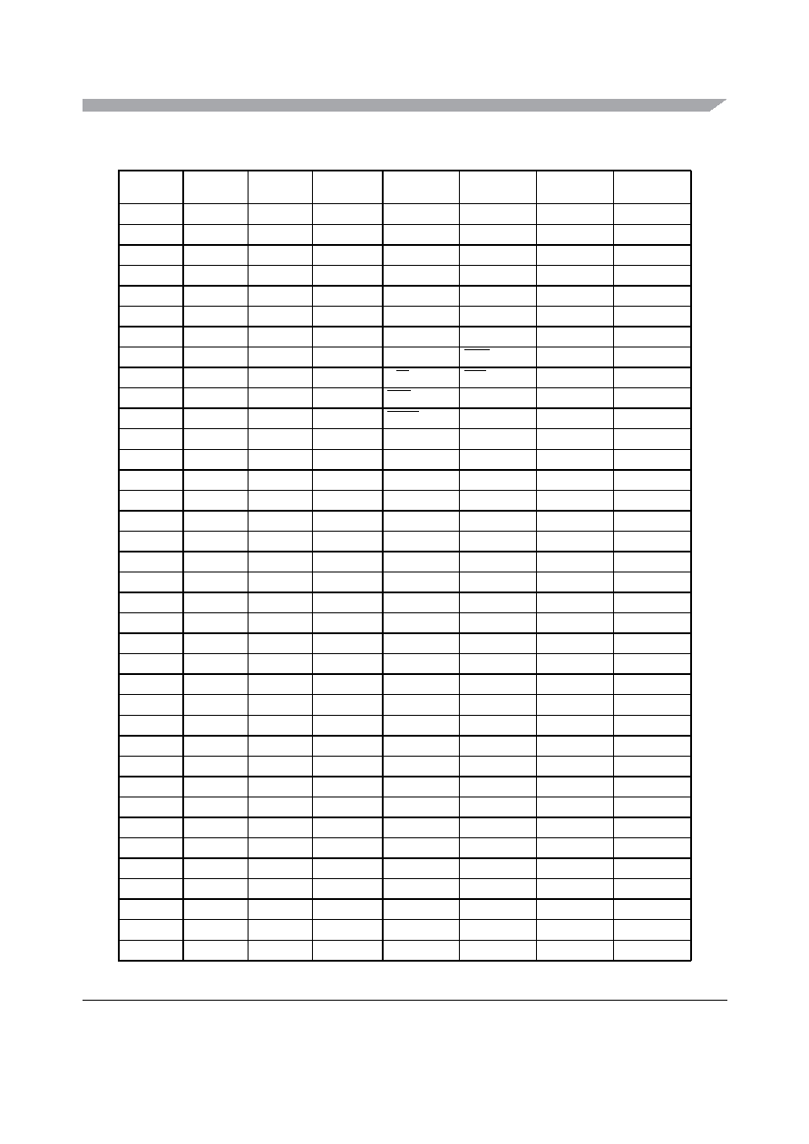
Table 1. Package and Memory Options of MC9S12
X
D Family Members
Device
Package
Flash
RAM
EEPROM
ROM
9S12XDP512
144 LQFP
512K
32K
4K
112 LQFP
9S12XDT512
144 LQFP
20K
112 LQFP
80 QFP
9S12XDT384
144 LQFP
384K
20K
112 LQFP
80 QFP
9S12XDQ256
144 LQFP
256K
16K
112 LQFP
80 QFP
9S12XDT256
144 LQFP
112 LQFP
80 QFP
9S12XD256
144 LQFP
14K
112 LQFP
80 QFP
3S12XDT256
144 LQFP
16K
(1)
NOTES:
1. No EEPROM is available on ROM versions.
256K
112 LQFP
80 QFP
9S12XDG128
112 LQFP
128K
12K
2K
80 QFP
3S12XDG128
112 LQFP
(1)
128K
80 QFP
9S12XD128
112 LQFP
128K
8K
2K
80 QFP
9S12XD64
80 QFP
64K
4K
1K

MC9S12XD Family, Rev. 2.14
12
Freescale Semiconductor
MC9S12XD Family Block Diagram
Table 2. Peripheral Options of MC9S12
X
D Family Members
Device
Package
XGATE
CAN
SCI
SPI
IIC
ECT
PIT
A/D
I/O
9S12XDP512
144LQFP
yes
5
6
3
2
8
4
2/24
119
112LQFP
5
4
3
1
8
4
2/16
91
9S12XDT512
144LQFP
3
6
3
1
8
4
2/24
119
112LQFP
3
4
3
1
8
4
2/16
91
80QFP
3
2
2
1
8
4
1/8
59
9S12XDT384
144LQFP
3
4
3
1
8
4
2/24
119
112LQFP
3
4
3
1
8
4
2/16
91
80QFP
3
2
2
1
8
4
1/8
59
9S12XDQ256
144LQFP
4
4
3
1
8
4
2/24
119
112LQFP
4
4
3
1
8
4
2/16
91
80QFP
4
2
2
1
8
4
1/8
59
9S12XDT256
144LQFP
3
4
3
1
8
4
2/24
119
112LQFP
3
4
3
1
8
4
2/16
91
80QFP
3
2
2
1
8
4
1/8
59
9S12XD256
144LQFP
1
4
2
1
8
4
2/24
119
112LQFP
1
4
2
1
8
4
2/16
91
80QFP
1
2
2
1
8
4
1/8
59
3S12XDT256
144LQFP
3
4
3
1
8
4
2/24
119
112LQFP
3
4
3
1
8
4
2/16
91
80QFP
3
2
2
1
8
4
1/8
59
9S12XDG128
112LQFP
yes
(1)
2
2
2
1
8
4
1/16
(2)
91
80QFP
2
2
2
1
8
4
1/8
59
3S12XDG128
112LQFP
2
2
2
1
8
4
1/16
(2)
91
80QFP
2
2
2
1
8
4
1/8
59
9S12XD128
112LQFP
1
2
2
1
8
4
1/16
(2)
91
80QFP
1
2
2
1
8
4
1/8
59
9S12XD64
80QFP
1
2
2
1
8
2
1/8
59
NOTES:
1. Can execute code only from RAM
2. ATD1 routed to PAD00-15 instead of PAD08-23.

MC9S12XD Family Block Diagram
MC9S12XD Family, Rev. 2.14
Freescale Semiconductor
13
Pinout explanations:
∑
A/D is the number of modules/total number of A/D channels.
∑
I/O is the sum of ports capable to act as digital input or output.
≠
144 Pin Packages:
Port A = 8, B = 8, C=8, D=8, E = 6 + 2 input only,
H = 8, J = 7, K = 8, M = 8, P = 8, S = 8, T = 8, PAD = 24
25 inputs provide Interrupt capability (H =8, P= 8, J = 7, IRQ, XIRQ)
≠
112 Pin Packages:
Port A = 8, B = 8, E = 6 + 2 input only, H = 8, J = 4, K = 7, M = 8, P = 8, S = 8, T = 8, PAD = 16
22 inputs provide Interrupt capability (H =8, P= 8, J = 4, IRQ, XIRQ)
≠
80 Pin Packages:
Port A = 8, B = 8, E = 6 + 2 input only, J = 2, M = 6, P = 7, S = 4, T = 8, PAD = 8
11 inputs provide Interrupt capability (P= 7, J = 2, IRQ, XIRQ)
∑
CAN0 can be routed under software control from PM[1:0] to pins PM[3:2] or PM[5:4] or PJ[7:6].
∑
CAN4 pins are shared between IIC0 pins.
∑
CAN4 can be routed under software control from PJ[7:6] to pins PM[5:4] or PM[7:6].
∑
Versions with 5 CAN modules will have CAN0, CAN1, CAN2, CAN3 and CAN4
∑
Versions with 4 CAN modules will have CAN0, CAN1, CAN2 and CAN4
∑
Versions with 3 CAN modules will have CAN0, CAN1 and CAN4.
∑
Versions with 2 CAN modules will have CAN0 and CAN4.
∑
Versions with 1 CAN modules will have CAN0
∑
Versions with 2 SPI modules will have SPI0 and SPI1.
∑
Versions with 4 SCI modules will have SCI0, SCI1, SCI2 and SCI4.
∑
Versions with 2 SCI modules will have SCI0 and SCI1.
∑
Versions with 1 IIC module will have IIC0.
∑
SPI0 can be routed to either Ports PS[7:4] or PM[5:2].
∑
SPI1 pins are shared with PWM[3:0]; In 144 and 112-pin versions, SPI1 can be routed under
software control to PH[3:0].
∑
SPI2 pins are shared with PWM[7:4]; In 144 and 112-pin versions, SPI2 can be routed under
software control to PH[7:4]. In 80-pin packages, SS-signal of SPI2 is not bonded out!

MC9S12XD Family, Rev. 2.14
14
Freescale Semiconductor
Pin Assignments
Pin Assignments
Table 3. Port and Peripheral Availability by Package Option
Port
144 LQFP
112 LQFP
80 QFP
Port AD/ADC Channels
24/24
16/16
8/8
Port A pins
8
8
8
Port B pins
8
8
8
Port C pins
8
0
0
Port D pins
8
0
0
Port E pins incl. IRQ/XIRQ input only
8
8
8
Port H pins
8
8
0
Port J pins
7
4
2
Port K pins
8
7
0
Port M pins
8
8
6
Port P pins
8
8
7
Port S pins
8
8
4
Port T pins
8
8
8
Sum of Ports
119
91
59
VDDX/VSSX
4/4
3/3
2/2
Table 4. Peripheral
≠
Port Cross Reference
(1)
C
A
N
0
C
A
N
1
C
A
N
2
C
A
N
3
C
A
N
4
S
C
I
0
S
C
I
1
S
C
I
2
S
C
I
3
S
C
I
4
S
C
I
5
S
P
I
0
S
P
I
1
S
P
I
2
I
I
C
0
I
I
C
1
PJ1:0
X
PJ3:2
PJ5:4
X
PJ7:6
O
X
X
PM1:0
X
PM3:2
O
X
O
PM5:4
O
X
O
PM7:6
X
O
X
PS1:0
X
PS3:2
X
PS7:4
X
PH3:0
O

Pin Assignments
MC9S12XD Family, Rev. 2.14
Freescale Semiconductor
15
PH5:4
X
O
PH7:6
X
O
PP3:0
X
PP7:4
X
NOTES:
1. X denotes the reset condition and O denotes a possible rerouting under software control
Table 5. Pin-Out Summary
(1)
LQFP
144
LQFP
112
QFP
80
Pin
2nd
Function
3rd
Function
4th
Function
5th
Function
1
1
1
PP3
KWP3
PWM3
SS1
2
2
2
PP2
KWP2
PWM2
SCK1
3
3
3
PP1
KWP1
PWM1
MOSI1
4
4
4
PP0
KWP0
PWM0
MISO1
5
PJ2
KWJ2
CS1
6
PK6
ADDR22
NOACC
7
5
PK3
ADDR19
8
6
PK2
ADDR18
IQSTAT2
9
7
PK1
ADDR17
IQSTAT1
10
8
PK0
ADDR16
IQSTAT0
11
9
5
PT0
IOC0
12
10
6
PT1
IOC1
13
11
7
PT2
IOC2
14
12
8
PT3
IOC3
15
13
9
VDD1
16
14
10
VSS1
17
15
11
PT4
IOC4
18
16
12
PT5
IOC5
19
17
13
PT6
IOC6
20
18
14
PT7
IOC7
21
19
PK5
ADDR21
22
20
PK4
ADDR20
23
21
PJ1
KWJ1
TXD2
24
22
PJ0
KWJ0
RXD2
Table 4. Peripheral
≠
Port Cross Reference
(1)
C
A
N
0
C
A
N
1
C
A
N
2
C
A
N
3
C
A
N
4
S
C
I
0
S
C
I
1
S
C
I
2
S
C
I
3
S
C
I
4
S
C
I
5
S
P
I
0
S
P
I
1
S
P
I
2
I
I
C
0
I
I
C
1

MC9S12XD Family, Rev. 2.14
16
Freescale Semiconductor
Pin Assignments
25
23
15
BKGD
MODC
26
VDDX2
27
VSSX2
28
PC0
DATA8
29
PC1
DATA9
30
PC2
DATA10
31
PC3
DATA11
32
24
16
PB0
ADDR0
UDS
33
25
17
PB1
ADDR1
34
26
18
PB2
ADDR2
35
27
19
PB3
ADDR3
36
28
20
PB4
ADDR4
37
29
21
PB5
ADDR5
38
30
22
PB6
ADDR6
39
31
23
PB7
ADDR7
40
PC4
DATA12
41
PC5
DATA13
42
PC6
DATA14
43
PC7
DATA15
44
32
PH7
KWH7
SS2
TXD5
45
33
PH6
KWH6
SCK2
RXD5
46
34
PH5
KWH5
MOSI2
TXD4
47
35
PH4
KWH4
MISO2
RXD4
48
36
24
PE7
XCLKS
ECLKX2
49
37
25
PE6
MODB
TAGHI
50
38
26
PE5
MODA
TAGLO
RE
51
39
27
PE4
ECLK
52
40
28
VSSR
53
41
29
VDDR
54
42
30
RESET
55
43
31
VDDPLL
56
44
32
XFC
57
45
33
VSSPLL
58
46
34
EXTAL
59
47
35
XTAL
60
48
36
TEST
61
49
PH3
KWH3
SS1
TXD7
Table 5. Pin-Out Summary
(1)
LQFP
144
LQFP
112
QFP
80
Pin
2nd
Function
3rd
Function
4th
Function
5th
Function
Pin Assignments
MC9S12XD Family, Rev. 2.14
Freescale Semiconductor
17
62
50
PH2
KWH2
SCK1
RXD7
63
51
PH1
KWH1
MOSI1
TXD6
64
52
PH0
KWH0
MISO1
RXD6
65
PD0
DATA0
66
PD1
DATA1
67
PD2
DATA2
68
PD3
DATA3
69
53
37
PE3
LSTRB
LDS
EROMCTL
70
54
38
PE2
RW
WE
71
55
39
PE1
IRQ
72
56
40
PE0
XIRQ
73
57
41
PA0
ADDR8
74
58
42
PA1
ADDR9
75
59
43
PA2
ADDR10
76
60
44
PA3
ADDR11
77
61
45
PA4
ADDR12
78
62
46
PA5
ADDR13
79
63
47
PA6
ADDR14
80
64
48
PA7
ADDR15
81
VDDX3
82
VDDX3
83
PD4
DATA4
84
PD5
DATA5
85
PD6
DATA6
86
PD7
DATA7
87
65
49
VDD2
88
66
50
VSS2
89
67
51
PAD00
AN0
90
68
PAD08
AN8
91
69
52
PAD01
AN1
92
70
PAD09
AN9
93
71
53
PAD02
AN2
94
72
PAD10
AN8
95
73
54
PAD03
AN3
96
74
PAD11
AN11
97
75
55
PAD04
AN4
98
76
PAD12
AN12
Table 5. Pin-Out Summary
(1)
LQFP
144
LQFP
112
QFP
80
Pin
2nd
Function
3rd
Function
4th
Function
5th
Function

MC9S12XD Family, Rev. 2.14
18
Freescale Semiconductor
Pin Assignments
99
77
56
PAD05
AN5
100
78
PAD13
AN13
101
79
57
PAD06
AN6
102
80
PAD14
AN14
103
81
58
PAD07
AN7
104
82
PAD15
AN15
105
PAD16
AN16
106
PAD17
AN17
107
83
59
VDDA
108
84
60
VRH
109
85
61
VRL
110
86
62
VSSA
111
PAD18
AN18
112
PAD19
AN19
113
PAD20
AN20
114
PAD21
AN21
115
PAD22
AN22
116
PAD23
AN23
117
87
PM7
TXCAN3
TXCAN4
TXD3
118
88
PM6
RXCAN3
RXCAN4
RXD3
119
89
63
PS0
RXD0
120
90
64
PS1
TXD0
121
91
65
PS2
RXD1
122
92
66
PS3
TXD1
123
93
PS4
MISO0
124
94
PS5
MOSI0
125
95
PS6
SCK0
126
96
PS7
SS0
127
97
67
VREGEN
128
98
68
PJ7
KWJ7
TXCAN4
SCL0
129
99
69
PJ6
KWJ6
RXCAN4
SDA0
130
PJ5
KWJ5
SCL1
CS2
131
PJ4
KWJ4
SDA1
CS0
132
100
70
PM5
TXCAN2
TXCAN0
TXCAN4
SCK0
133
101
71
PM4
RXCAN2
RXCAN0
RXCAN4
MOSI0
134
102
72
PM3
TXCAN1
TXCAN0
SS0
135
103
73
PM2
RXCAN1
RXCAN0
MISO0
Table 5. Pin-Out Summary
(1)
LQFP
144
LQFP
112
QFP
80
Pin
2nd
Function
3rd
Function
4th
Function
5th
Function

Pin Assignments
MC9S12XD Family, Rev. 2.14
Freescale Semiconductor
19
136
104
74
PM1
TXCAN0
137
105
75
PM0
RXCAN0
138
106
76
VSSX1
139
107
77
VDDX1
140
108
PK7
ROMCTL
EWAIT
141
109
78
PP7
KWP7
PWM7
SCK2
142
110
PP6
KWP6
PWM6
SS2
143
111
79
PP5
KWP5
PWM5
MOSI2
144
112
80
PP4
KWP4
PWM4
MISO2
NOTES:
1. Table shows a superset of pin functions. Not all functions are available on all derivatives
Table 5. Pin-Out Summary
(1)
LQFP
144
LQFP
112
QFP
80
Pin
2nd
Function
3rd
Function
4th
Function
5th
Function

MC9S12XD Family, Rev. 2.14
20
Freescale Semiconductor
Pin Assignments
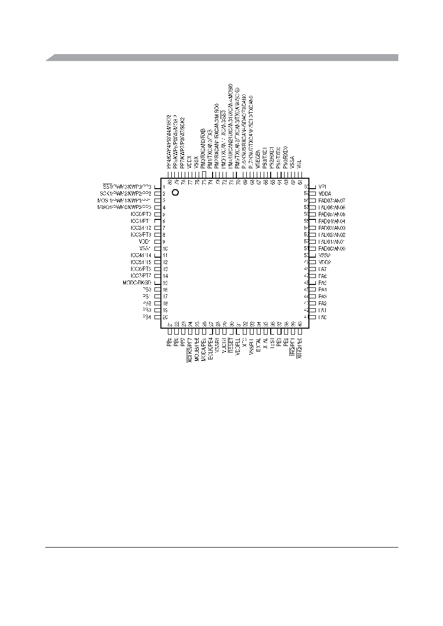
Figure 1. MC9S12
X
D Family Pin Assignments for 144-pin LQFP Package
MC9S12
X
D Family
144 LQFP
Pins shown in BOLD are not available on the 80 QFP package
1
2
3
4
5
6
7
8
9
10
11
12
13
14
15
16
17
18
19
20
21
22
23
24
25
26
27
28
29
30
31
32
33
34
35
36
3
7
3
8
3
9
4
0
4
1
4
2
4
3
4
4
4
5
4
6
4
7
4
8
4
9
5
0
5
1
5
2
5
3
5
4
5
5
5
6
5
7
5
8
5
9
6
0
6
1
6
2
6
3
6
4
6
5
6
6
6
7
6
8
6
9
7
0
7
1
7
2
108
107
106
105
104
103
102
101
100
99
98
97
96
95
94
93
92
91
90
89
88
87
86
85
84
83
82
81
80
79
78
77
76
75
74
73
1
4
4
1
4
3
1
4
2
1
4
1
1
4
0
1
3
9
1
3
8
1
3
7
1
3
6
1
3
5
1
3
4
1
3
3
1
3
2
1
3
1
1
3
0
1
2
9
1
2
8
1
2
7
1
2
6
1
2
5
1
2
4
1
2
3
1
2
2
1
2
1
1
2
0
1
1
9
1
1
8
1
1
7
1
1
6
1
1
5
1
1
4
1
1
3
1
1
2
1
1
1
1
1
0
1
0
9
Pins shown in BOLD-ITALICS are bit available on the 112 LQFP
nor on the 80 QFP Package Option

Pin Assignments
MC9S12XD Family, Rev. 2.14
Freescale Semiconductor
21
Figure 2. MC9S12
X
D Family Pin Assignments for 112-pin LQFP Package
MC9S12
X
D Family
112LQFP
Pins shown in BOLD are not available on the 80 QFP package
MC9S12XD Family, Rev. 2.14
22
Freescale Semiconductor
Pin Assignments
Figure 3. MC9S12
X
D Family Pin Assignments for 80-pin QFP Package
MC9S12
X
D Family
80-Pin QFP

Memory Maps
MC9S12XD Family, Rev. 2.14
Freescale Semiconductor
23
Memory Maps
Figure 4. MC9S12XD-Family Memory Map
1
1. The memory Map shows the memory sizes of DP512 part. For memory configuration of other parts see
Table 1
.
NORMAL
SINGLE CHIP
EXPANDED
SPECIAL
SINGLE CHIP
VECTORS
16K Fixed Flash EEPROM
2K, 4K, 8K or 16K Protected Boot Sector
16K Page Window
32 * 16K Flash EEPROM Pages
16K Fixed Flash EEPROM
2K Register Space
32K Bytes RAM
8 * 4K pages accessible through $1000 - $1FFF
4K Bytes EEPROM
4 * 1K pages accessible through $0800 - $0BFF
VECTORS
E
x
t
e
r
n
a
l
BDM
$0000
$FFFF
$C000
$8000
$4000
$0800
$1000
$FF00
$2000
$0C00

MC9S12XD Family, Rev. 2.14
24
Freescale Semiconductor
Memory Maps
Figure 5. MC9S12XD-Family Flash Configuration
1, 2, 3, 4, 5
1. XGATE read access to Flash not possible on DG128/D128 and D64
2. Program Pages available on DT384 are $E0 - $E7 and $F0 - $FF
3. Program Pages available on DQ256/D256 are $E0 - $E7 and $F8 - $FF
4. Shared XGATE/CPU area on DP512/DT512/DT384 at global address $78_0800 to $78_FFFF (30Kbyte)
5. Shared XGATE/CPU area on DQ256/D256 at global address $78_0800 to $79_3FFF (46Kbyte)
Shared XGATE/CPU area
Not implemented
$78_0000 (PPAGE $E0)
Global Address
$7A_0000 (PPAGE $E8)
$7C_0000 (PPAGE $F0)
$7E_0000 (PPAGE $F8)
128K
64K
128K
128K
128K
128K
128K
128K
128K
128K
128K
DP512/
DT512
DT384
DQ256/
D256
DG128/
D128
D64

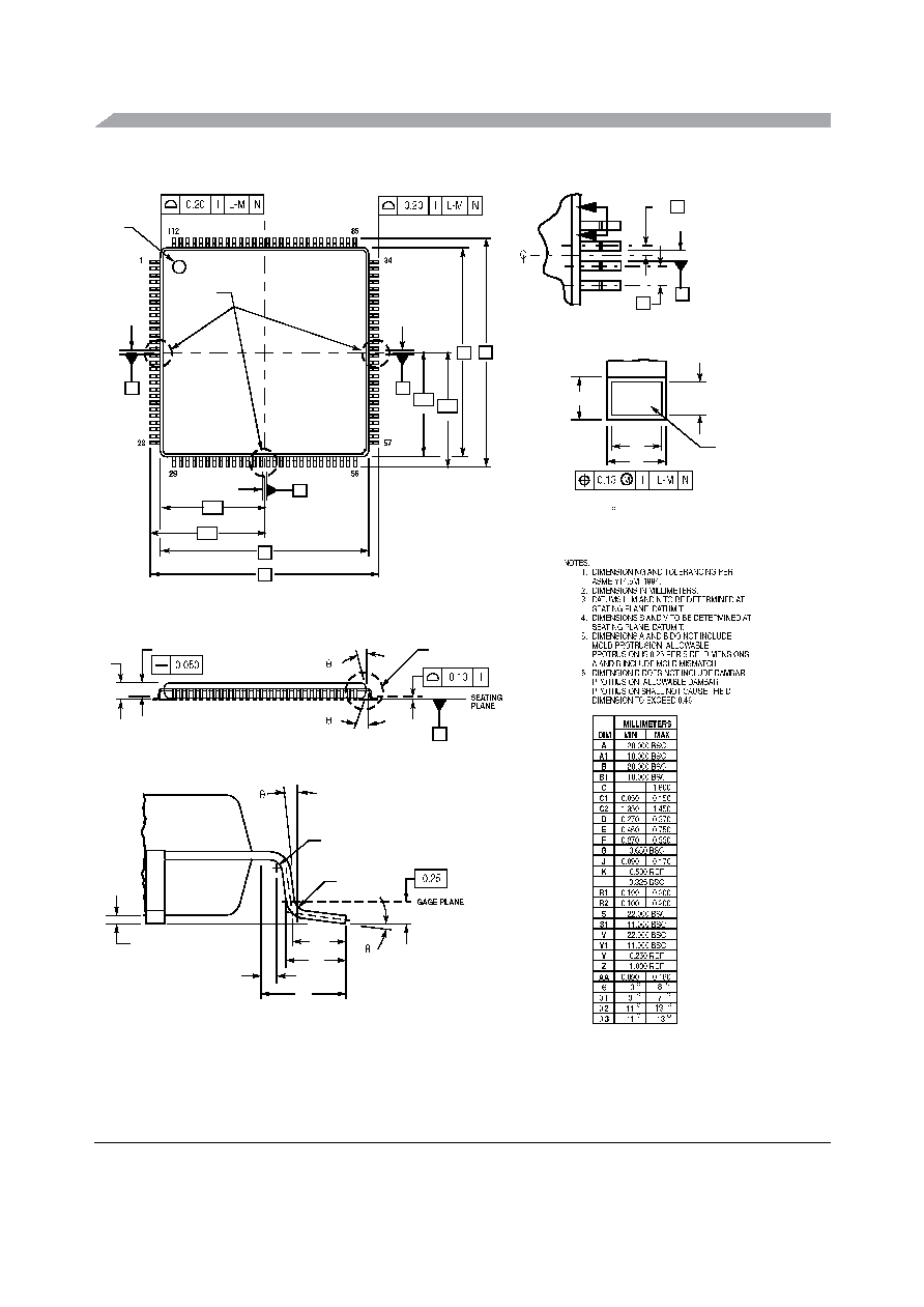
Mechanical Package Dimensions
MC9S12XD Family, Rev. 2.14
Freescale Semiconductor
25
Mechanical Package Dimensions
Figure 6. 144-pin LQFP Mechanical Dimensions (case no. 918-03)
N
0.20 T L-M
144
GAGE PLANE
73
109
37
SEATING
108
1
36
72
PLANE
4X
4X 36 TIPS
PIN 1
IDENT
VIEW Y
B
B1 V1
A1
S1
V
P
G
A
S
0.1
C
2
VIEW AB
J1
J1
140X
4X
VIEW Y
PLATING
F
AA
J
D
BASE
METAL
SECTION J1-J1
(ROTATED 90 )
144 PL
N
0.08
M
T L-M
DIM
A
MIN
MAX
20.00 BSC
MILLIMETERS
A1
10.00 BSC
B
20.00 BSC
B1
10.00 BSC
C
1.40
1.60
C1
0.05
0.15
C2
1.35
1.45
D
0.17
0.27
E
0.45
0.75
F
0.17
0.23
G
0.50 BSC
J
0.09
0.20
K
0.50 REF
P
0.25 BSC
R1
0.13
0.20
R2
0.13
0.20
S
22.00 BSC
S1
11.00 BSC
V
22.00 BSC
V1
11.00 BSC
Y
0.25 REF
Z
1.00 REF
AA
0.09
0.16
0
0
7
11
13
1
2
NOTES:
1.
DIMENSIONS AND TOLERANCING PER ASME
Y14.5M, 1994.
2.
DIMENSIONS IN MILLIMETERS.
3.
DATUMS L, M, N TO BE DETERMINED AT THE
SEATING PLANE, DATUM T.
4.
DIMENSIONS S AND V TO BE DETERMINED
AT SEATING PLANE, DATUM T.
5.
DIMENSIONS A AND B DO NOT INCLUDE
MOLD PROTRUSION. ALLOWABLE
PROTRUSION IS 0.25 PER SIDE. DIMENSIONS
A AND B DO INCLUDE MOLD MISMATCH
AND ARE DETERMINED AT DATUM PLANE H.
6.
DIMENSION D DOES NOT INCLUDE DAMBAR
PROTRUSION. ALLOWABLE DAMBAR
PROTRUSION SHALL NOT CAUSE THE D
DIMENSION TO EXCEED 0.35.
0.05
CL
(Z)
R2
E
C2
(Y)
R1
(K)
C1
1
0.25
VIEW AB
N
0.20 T L-M
M
L
N
2
T
T
144X
X
MC9S12XD Family, Rev. 2.14
26
Freescale Semiconductor
Mechanical Package Dimensions
Figure 7. 112-pin LQFP Mechanical Dimensions (case no. 987)
---
P
VIEW Y
4X
4X 28 TIPS
PIN 1
DENT
B
V
V1
B1
A1
S1
A
S
VIEW AB
3
C
C2
2
1
VIEW AB
C1
(Z)
(Y)
E
(K)
R2
R1
J1
VIEW Y
J1
P
G
108X
4X
SECTION J1-J1
BASE
ROTATED 90 COUNTERCLOCKWISE
METAL
J
AA
F
D
L
N
M
T
112X
X
X=L, M OR N
R
R
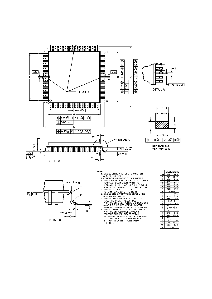
Figure 8. 80-pin QFP Mechanical Dimensions (case no. 841B)

9S12XDFAMPP
Rev. 2.14, 7-Nov-2005
How to Reach Us:
Home Page:
www.freescale.com
E-mail:
support@freescale.com
USA/Europe or Locations Not Listed:
Freescale Semiconductor
Technical Information Center, CH370
1300 N. Alma School Road
Chandler, Arizona 85224
+1-800-521-6274 or +1-480-768-2130
support@freescale.com
Europe, Middle East, and Africa:
Freescale Halbleiter Deutschland GmbH
Technical Information Center
Schatzbogen 7
81829 Muenchen, Germany
+44 1296 380 456 (English)
+46 8 52200080 (English)
+49 89 92103 559 (German)
+33 1 69 35 48 48 (French)
support@freescale.com
Japan:
Freescale Semiconductor Japan Ltd.
Headquarters
ARCO Tower 15F
1-8-1, Shimo-Meguro, Meguro-ku,
Tokyo 153-0064
Japan
0120 191014 or +81 3 5437 9125
support.japan@freescale.com
Asia/Paci
c:
Freescale Semiconductor Hong Kong Ltd.
Technical Information Center
2 Dai King Street
Tai Po Industrial Estate
Tai Po, N.T., Hong Kong
+800 2666 8080
support.asia@freescale.com
For Literature Requests Only:
Freescale Semiconductor Literature Distribution Center
P.O. Box 5405
Denver, Colorado 80217
1-800-441-2447 or 303-675-2140
Fax: 303-675-2150
LDCForFreescaleSemiconductor@hibbertgroup.com
Information in this document is provided solely to enable system and software
implementers to use Freescale Semiconductor products. There are no express or
implied copyright licenses granted hereunder to design or fabricate any integrated
circuits or integrated circuits based on the information in this document.
Freescale Semiconductor reserves the right to make changes without further notice to
any products herein. Freescale Semiconductor makes no warranty, representation or
guarantee regarding the suitability of its products for any particular purpose, nor does
Freescale Semiconductor assume any liability arising out of the application or use of any
product or circuit, and speci
cally disclaims any and all liability, including without
limitation consequential or incidental damages.
"
Typical
"
parameters that may be
provided in Freescale Semiconductor data sheets and/or speci
cations can and do vary
in different applications and actual performance may vary over time. All operating
parameters, including
"
Typicals
"
, must be validated for each customer application by
customer
'
s technical experts. Freescale Semiconductor does not convey any license
under its patent rights nor the rights of others. Freescale Semiconductor products are
not designed, intended, or authorized for use as components in systems intended for
surgical implant into the body, or other applications intended to support or sustain life,
or for any other application in which the failure of the Freescale Semiconductor product
could create a situation where personal injury or death may occur. Should Buyer
purchase or use Freescale Semiconductor products for any such unintended or
unauthorized application, Buyer shall indemnify and hold Freescale Semiconductor and
its of
cers, employees, subsidiaries, af
liates, and distributors harmless against all
claims, costs, damages, and expenses, and reasonable attorney fees arising out of,
directly or indirectly, any claim of personal injury or death associated with such
unintended or unauthorized use, even if such claim alleges that Freescale
Semiconductor was negligent regarding the design or manufacture of the part.
Freescale
TM
and the Freescale logo are trademarks of Freescale Semiconductor, Inc.
All other product or service names are the property of their respective owners.
©
Freescale Semiconductor, Inc. 2005. All rights reserved.