
56F8000
16-bit Digital Signal Controllers
freescale.com
56F8013
Data Sheet
Preliminary Technical Data
MC56F8013
Rev. 2
4/2005

56F8013 Technical Data, Rev. 2
2
Freescale Semiconductor
Preliminary
Document Revision History
Version History
Description of Change
Rev 0
Initial release
Rev 1
Updates to
Part 10, Specifications,
Table 10-1
, added maximum clamp current , per pin
Table 10-12
, clarified variation over temperature table and graph
Table 10-16
, added LIN slave timing
Rev 2
Added alternate pins to
Figure 11-1
and
Table 11-1
.
Please see http://www.freescale.com for the most current Data Sheet revision.
56F8013 Technical Data, Rev. 2
Freescale Semiconductor
3
Preliminary
56F8013 Block Diagram
Program Controller
and Hardware
Looping Unit
Data ALU
16 x 16 + 36 -> 36-Bit MAC
Three 16-bit Input Registers
Four 36-bit Accumulators
Address
Generation Unit
Bit
Manipulation
Unit
16-Bit
56800E Core
Interrupt
Controller
4
Unified Data /
Program RAM
4KB
PDB
PDB
XAB1
XAB2
XDB2
CDBR
SPI or I
2
C
or Timer
or GPIOB
IPBus Bridge (IPBB)
System Bus
Control
R/W Control
Memory
PAB
PAB
CDBW
CDBR
CDBW
JTAG/EOnCE
Port or
GPIOD
Digital Reg
Analog Reg
Low-Voltage
Supervisor
V
CAP
V
DD
V
SS_IO
V
DDA
V
SSA
4
RESET
7
Timer or
GPIOB
AD0
2
3
Clock
Generator*
System
Integration
Module
P
O
R
O
S
C
PWM Outputs
PWM
or Timer Port
or GPIOA
*Includes On-Chip
Relaxation Oscillator
COP/
Watchdog
AD1
3
Program Memory
8K x 16 Flash
ADC
or
GPIOC
SCI
or I
2
C
or GPIOB
2
2
∑ Up to 32 MIPS at 32MHz core frequency
∑ DSP and MCU functionality in a unified,
C-efficient architecture
∑ 16KB Program Flash
∑ 4KB Unified Data/Program RAM
∑ One 6-channel PWM module
∑ One 6-channel 12-bit ADC
∑ One Serial Communication Interface (SCI) with LIN
slave functionality
∑ One Serial Peripheral Interface (SPI)
∑ One 16-bit Quad Timer
∑ One Inter-Integrated Circuit (I
2
C) Port
∑ Computer Operating Properly (COP)/Watchdog
∑ On-Chip Relaxation Oscillator
∑ Integrated Power-On Reset and Low-Voltage Interrupt
Module
∑ JTAG/Enhanced On-Chip Emulation (OnCETM) for
unobtrusive, real-time debugging
∑ Up to 26 GPIO lines
∑ 32-pin LQFP Package
56F8013 General Description

56F8013 Technical Data, Rev. 2
4
Freescale Semiconductor
Preliminary
Part 1: Overview . . . . . . . . . . . . . . . . . . . . . . 5
1.1. 56F8013 Features . . . . . . . . . . . . . . . . . . . . . 5
1.2. 56F8013 Description . . . . . . . . . . . . . . . . . . . 6
1.3. Award-Winning Development Environment . . 7
1.4. Architecture Block Diagram . . . . . . . . . . . . . 7
1.5. Product Documentation . . . . . . . . . . . . . . . . 11
1.6. Data Sheet Conventions. . . . . . . . . . . . . . . 11
Part 2: Signal/Connection Descriptions . . . 12
2.1. Introduction . . . . . . . . . . . . . . . . . . . . . . . . . 12
2.2. 56F8013 Signal Pins . . . . . . . . . . . . . . . . . . 16
Part 3: OCCS . . . . . . . . . . . . . . . . . . . . . . . . . 24
3.1. Overview . . . . . . . . . . . . . . . . . . . . . . . . . . . 24
3.2. Features . . . . . . . . . . . . . . . . . . . . . . . . . . . 24
3.3. Operating Modes . . . . . . . . . . . . . . . . . . . . . 24
3.4. Block Diagram . . . . . . . . . . . . . . . . . . . . . . 26
3.5. Pin Descriptions . . . . . . . . . . . . . . . . . . . . . . 27
Part 4: Memory Map . . . . . . . . . . . . . . . . . . . 27
4.1. Introduction . . . . . . . . . . . . . . . . . . . . . . . . . 27
4.2. Interrupt Vector Table . . . . . . . . . . . . . . . . . 27
4.3. Program Map . . . . . . . . . . . . . . . . . . . . . . . 29
4.4. Data Map . . . . . . . . . . . . . . . . . . . . . . . . . . . 30
4.5. EOnCE Memory Map . . . . . . . . . . . . . . . . . . 31
4.6. Peripheral Memory Mapped Registers . . . . 32
Part 5: Interrupt Controller (ITCN) . . . . . . . . 42
5.1. Introduction . . . . . . . . . . . . . . . . . . . . . . . . . 42
5.2. Features . . . . . . . . . . . . . . . . . . . . . . . . . . . 42
5.3. Functional Description . . . . . . . . . . . . . . . . . 42
5.4. Block Diagram . . . . . . . . . . . . . . . . . . . . . . . 44
5.5. Operating Modes . . . . . . . . . . . . . . . . . . . . . 44
5.6. Register Descriptions . . . . . . . . . . . . . . . . . . 45
5.7. Resets . . . . . . . . . . . . . . . . . . . . . . . . . . . . . 61
Part 6: System Integration Module (SIM) . . 62
6.1. Introduction . . . . . . . . . . . . . . . . . . . . . . . . . 62
6.2. Features . . . . . . . . . . . . . . . . . . . . . . . . . . . 62
6.3. Register Descriptions . . . . . . . . . . . . . . . . . . 63
6.4. Clock Generation Overview . . . . . . . . . . . . . 76
6.5. Power-Down Modes . . . . . . . . . . . . . . . . . . 77
6.6. Resets . . . . . . . . . . . . . . . . . . . . . . . . . . . . . 78
6.7. Clocks . . . . . . . . . . . . . . . . . . . . . . . . . . . . . 80
6.8. Interrupts . . . . . . . . . . . . . . . . . . . . . . . . . . 81
Part 7: Security Features . . . . . . . . . . . . . . .82
7.1. Operation with Security Enabled . . . . . . . . . 82
7.2. Flash Access Lock and Unlock Mechanisms 82
Part 8: General Purpose Input/Output
(GPIO) . . . . . . . . . . . . . . . . . . . . . . . . . . . . . . .84
8.1. Introduction . . . . . . . . . . . . . . . . . . . . . . . . . 84
8.2. Configuration . . . . . . . . . . . . . . . . . . . . . . . . 84
8.3. Reset Values . . . . . . . . . . . . . . . . . . . . . . . . 86
Part 9: Joint Test Action Group (JTAG) . . .91
9.1. 56F8013 Information . . . . . . . . . . . . . . . . . . 91
Part 10: Specifications. . . . . . . . . . . . . . . . . 91
10.1. General Characteristics . . . . . . . . . . . . . . . 91
10.2. DC Electrical Characteristics . . . . . . . . . . . 95
10.3. AC Electrical Characteristics . . . . . . . . . . . 98
10.4. Flash Memory Characteristics . . . . . . . . . . 98
10.5. External Clock Operation Timing . . . . . . . . 99
10.6. Phase Locked Loop Timing . . . . . . . . . . . . 99
10.7. Relaxation Oscillator Timing . . . . . . . . . . 100
10.8. Reset, Stop, Wait, Mode Select, and
Interrupt Timing . . . . . . . . . . . . . . 101
10.9. Serial Peripheral Interface (SPI) Timing . 102
10.10. Quad Timer Timing . . . . . . . . . . . . . . . . 105
10.11. Serial Communication Interface
(SCI) Timing . . . . . . . . . . . . . . . . 106
10.12. Inter-Integrated Circuit Interface
(I2C) Timing . . . . . . . . . . . . . . . . 107
10.13. JTAG Timing . . . . . . . . . . . . . . . . . . . . . 108
10.14. Analog-to-Digital Converter
(ADC) Parameters . . . . . . . . . . . 109
10.15. Equivalent Circuit for ADC Inputs . . . . . 111
10.16. Power Consumption . . . . . . . . . . . . . . . 112
Part 11: Packaging . . . . . . . . . . . . . . . . . . .114
11.1. 56F8013 Package and Pin-Out Information 114
Part 12: Design Considerations . . . . . . . . .117
12.1. Thermal Design Considerations . . . . . . . . 117
12.2. Electrical Design Considerations . . . . . . . 118
Part 13: Ordering Information . . . . . . . . . . 119
Part 14: Appendix . . . . . . . . . . . . . . . . . . . .120
56F8013 Data Sheet Table of Contents

56F8013 Features
56F8013 Technical Data, Rev. 2
Freescale Semiconductor
5
Preliminary
Part 1 Overview
1.1 56F8013 Features
1.1.1
Digital Signal Controller Core
∑
Efficient 16-bit 56800E family Digital Signal Controller (DSC) engine with dual Harvard architecture
∑
As many as 32 Million Instructions Per Second (MIPS) at 32MHz core frequency
∑
Single-cycle 16
◊ 16-bit parallel Multiplier-Accumulator (MAC)
∑
Four 36-bit accumulators, including extension bits
∑
Arithmetic and logic multi-bit shifter
∑
Parallel instruction set with unique DSP addressing modes
∑
Hardware DO and REP loops
∑
Three internal address buses
∑
Four internal data buses
∑
Instruction set supports both DSP and controller functions
∑
Controller-style addressing modes and instructions for compact code
∑
Efficient C compiler and local variable support
∑
Software subroutine and interrupt stack with depth limited only by memory
∑
JTAG/EOnCE debug programming interface
1.1.2
Memory
∑
Harvard architecture permits as many as three simultaneous accesses to program and data memory
∑
Flash security and protection
∑
On-chip memory, including a low-cost, high-volume Flash solution
-- 16KB of Program Flash
-- 4KB of Unified Data/Program RAM
∑
EEPROM emulation capability
1.1.3
Peripheral Circuits for 56F8013
∑
One Pulse Width Modulator (PWM) module with six PWM outputs and four Fault inputs; fault-tolerant
design with dead time insertion; supports both center-aligned and edge-aligned modes
∑
One six-input, 12-bit, Analog-to-Digital Converter (ADC), which support two simultaneous conversions
with dual, 3-pin multiplexed inputs; ADC and PWM modules can be synchronized through Timer Channels
2 and 3
∑
One 16-bit Quad Timer module (TMR) totaling four pins: Timer works in conjunction with the PWM and
ADC
∑
One Serial Communication Interface (SCI) with LIN Slave functionality
∑
One Serial Peripheral Interface (SPI)
∑
Computer Operating Properly (COP)/Watchdog timer

56F8013 Technical Data, Rev. 2
6
Freescale Semiconductor
Preliminary
∑
26
General Purpose I/O (GPIO) pins
∑
Integrated Power-On Reset and Low-Voltage Interrupt Module
∑
One Inter-Integrated Circuit (I
2
C) port
∑
JTAG/Enhanced On-Chip Emulation (OnCE) for unobtrusive, processor speed-independent, real-time
debugging
∑
Fixed Phase Lock Loop (PLL)
∑
On-chip relaxation oscillator
1.1.4
Energy Information
∑
Fabricated in high-density CMOS with 5V-tolerant, TTL-compatible digital inputs
∑
On-chip regulators for digital and analog circuitry to lower cost and reduce noise
∑
Wait and Stop modes available
∑
ADC smart power management
∑
Each peripheral can be individually disabled to save power
1.2 56F8013 Description
The 56F8013 is a member of the 56800E core-based family of Digital Signal Controllers (DSCs). It
combines, on a single chip, the processing power of a DSP and the functionality of a microcontroller with
a flexible set of peripherals to create an extremely cost-effective solution. Because of its low cost,
configuration flexibility, and compact program code, the 56F8013 is well-suited for many applications.
The 56F8013 includes many peripherals that are especially useful for industrial control, motion control,
home appliances, general purpose inverters, smart sensors, fire and security systems, power management,
and medical monitoring applications.
The 56800E core is based on a Harvard-style architecture consisting of three execution units operating in
parallel, allowing as many as six operations per instruction cycle. The MCU-style programming model and
optimized instruction set allow straightforward generation of efficient, compact DSP and control code.
The instruction set is also highly efficient for C compilers to enable rapid development of optimized
control applications.
The 56F8013 supports program execution from internal memories. Two data operands can be accessed
from the on-chip data RAM per instruction cycle. The 56F8013 also offers up to 26 General Purpose
Input/Output (GPIO) lines, depending on peripheral configuration.
The 56F8013 Digital Signal Controller includes 16KB of Program Flash and 4KB of Unified
Data/Program RAM. Program Flash memory can be independently bulk erased or erased in pages.
Program Flash page erase size is 512 Bytes/256 Words.
A key application-specific feature of the 56F8013 is the inclusion of one Pulse Width Modulator (PWM)
module. This module incorporates three complementary, individually programmable PWM signal output
pairs and is also capable of supporting six independent PWM functions to enhance motor control
functionality. Complementary operation permits programmable dead time insertion, and separate top and
bottom output polarity control. The up-counter value is programmable to support a continuously variable

Award-Winning Development Environment
56F8013 Technical Data, Rev. 2
Freescale Semiconductor
7
Preliminary
PWM frequency. Edge-aligned and center-aligned synchronous pulse width control (0% to 100%
modulation) is supported. The device is capable of controlling most motor types: ACIM (AC Induction
Motors), both BDC and BLDC (Brush and Brushless DC motors), SRM and VRM (Switched and Variable
Reluctance Motors), and stepper motors. The PWM incorporates fault protection and cycle-by-cycle
current limiting with sufficient output drive capability to directly drive standard optoisolators. A
"smoke-inhibit", write-once protection feature for key parameters is also included. A patented PWM
waveform distortion correction circuit is also provided. Each PWM is double-buffered and includes
interrupt controls to permit integral reload rates to be programmable from 1/2 (center-aligned mode only)
to 16. The PWM module provides reference outputs to synchronize the Analog-to-Digital Converter
(ADC) through Quad Timer, Channels 2 and 3.
This Digital Signal Controller also provides a full set of standard programmable peripherals that include
one Serial Communications Interface (SCI), one Serial Peripheral Interface (SPI), one Quad Timer, and
one Inter-Integrated Circuit (I
2
C) interface. Any of these interfaces can also be used as General Purpose
Input/Outputs (GPIOs).
1.3 Award-Winning Development Environment
Processor Expert
TM
(PE) provides a Rapid Application Design (RAD) tool that combines easy-to-use
component-based software application creation with an expert knowledge system.
The CodeWarrior Integrated Development Environment is a sophisticated tool for code navigation,
compiling, and debugging. A complete set of evaluation modules (EVMs), demonstration board kit and
development system cards will support concurrent engineering. Together, PE, CodeWarrior and EVMs
create a complete, scalable tools solution for easy, fast, and efficient development.
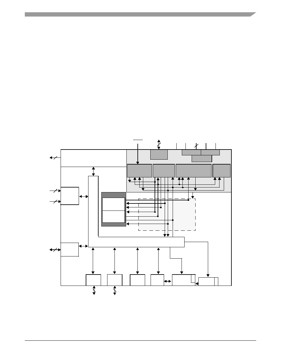
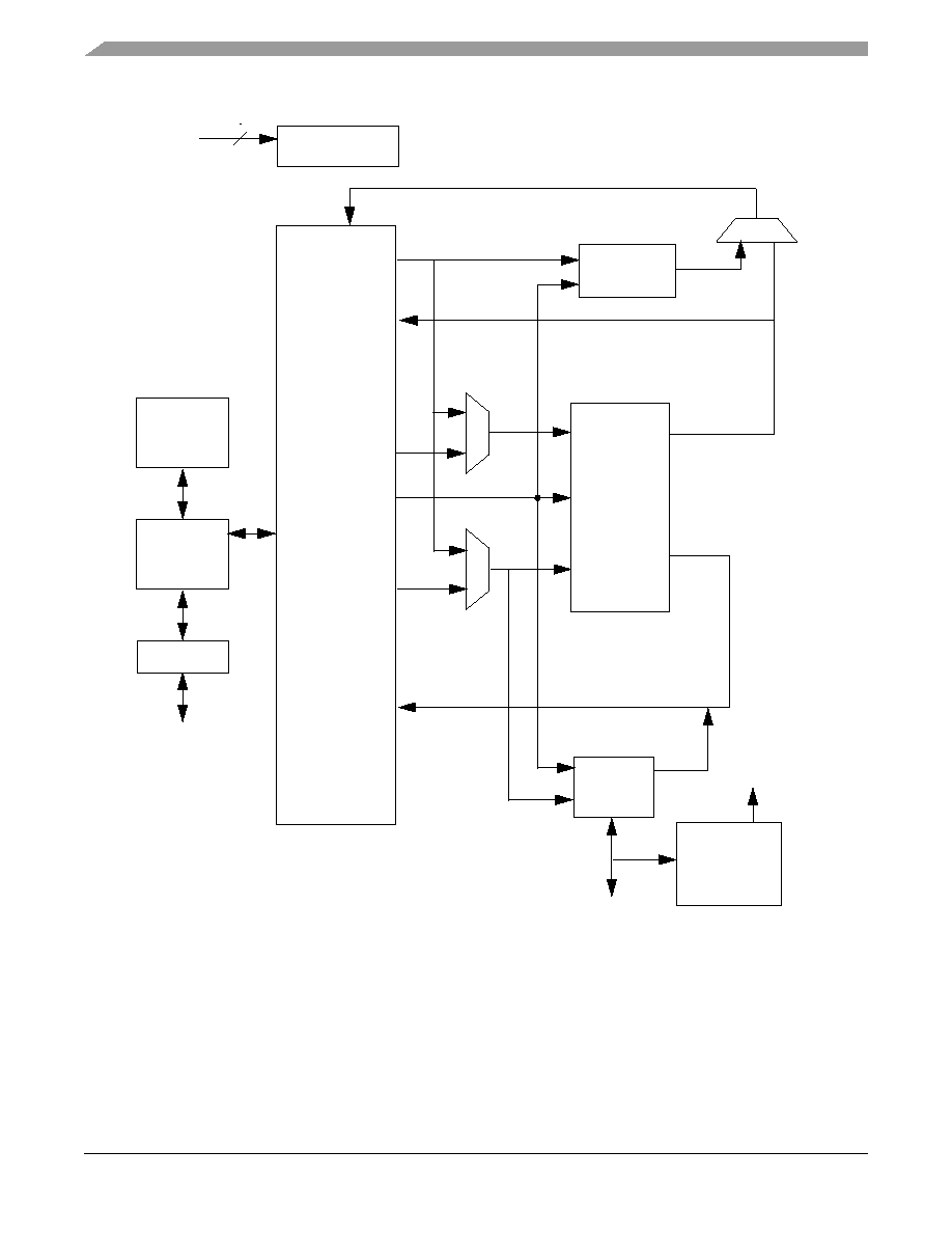
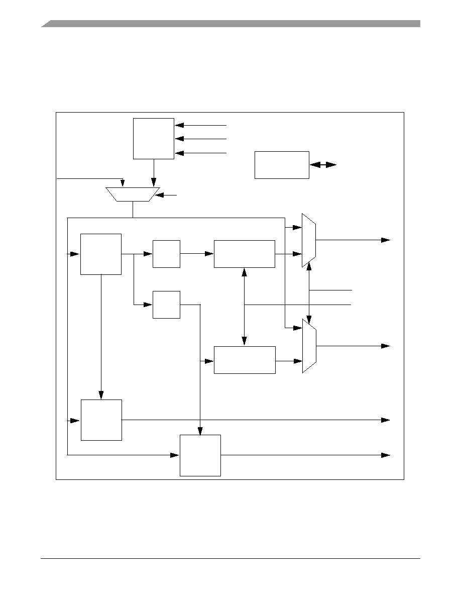
1.4 Architecture Block Diagram
The 56F8013's architecture is shown in
Figure 1-1
,
Figure 1-2
, and
Figure 1-3
.
Figure 1-1
illustrates
how the 56800E system buses communicate with internal memories and the IPBus Bridge.
Table 1-1
lists
the internal buses in the 56800E architecture and provides a brief description of their function.
Figure 1-2
and
Figure 1-3
show the peripherals and control blocks connected to the IPBus Bridge. The figures do not
show the on-board regulator and power and ground signals. They also do not show the multiplexing
between peripherals or the dedicated GPIOs. Please see
Part 2 Signal/Connection Descriptions
to see
which signals are multiplexed with those of other peripherals.
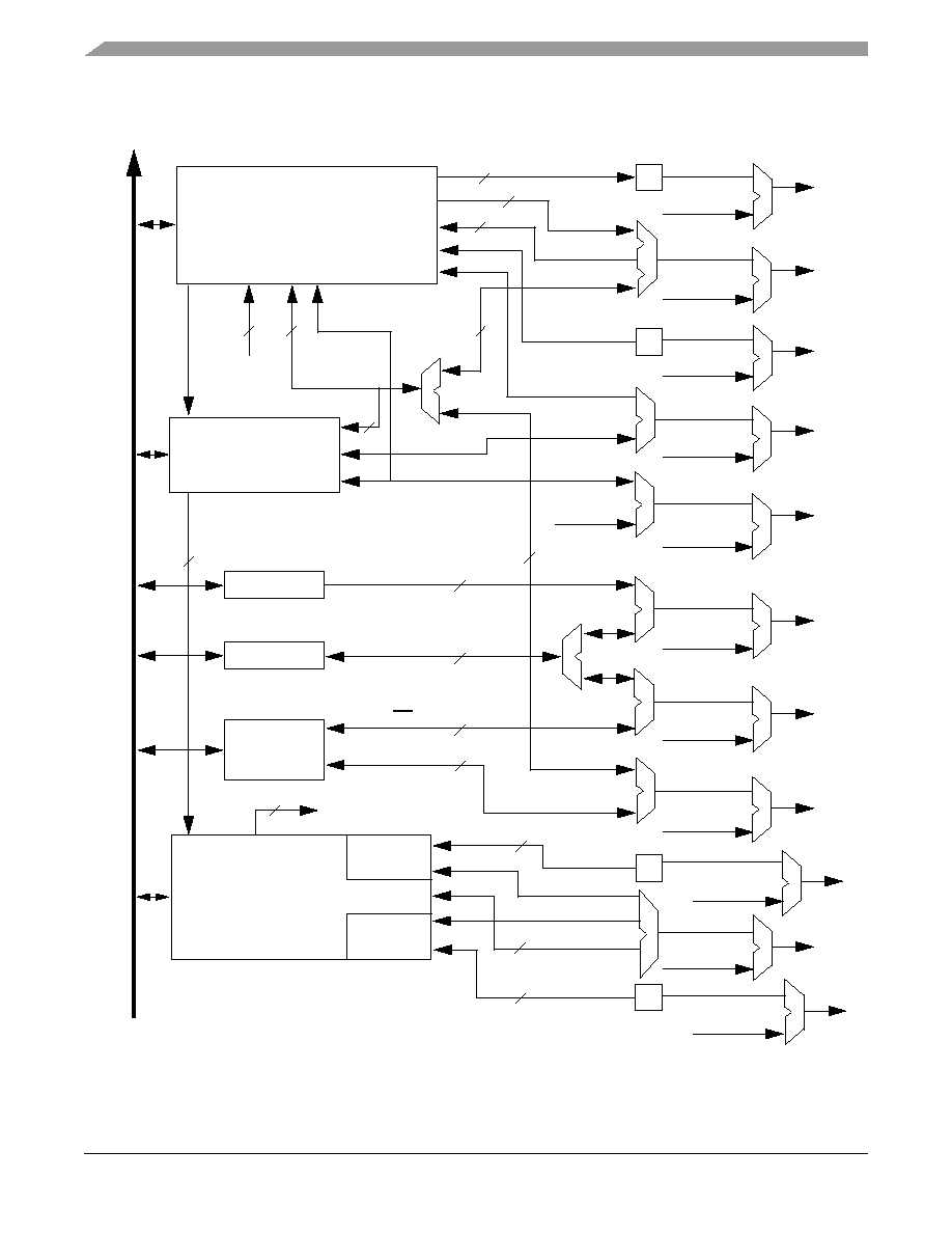
1.4.1
PWM, TMR and ADC Connections
Figure 1-3
shows the over/under voltage connections from the ADC to the PWM and the connections to
the PWM from the TMR and GPIO. These signals can control the PWM outputs in a similar manner to the
over/under voltage control signals. See the 56F8000 Peripheral Reference Manual for additional
information.
The PWM_reload_sync output can be connected to the TMR channel 3 input and the TMR channels 2 and
3 outputs are connected to the ADC sync inputs. These are controlled by bits in the SIM Control Register;
see
Section 6.3.1
.
56F8013 Technical Data, Rev. 2
8
Freescale Semiconductor
Preliminary
Figure 1-1 System Bus Interfaces
Note:
Flash memories are encapsulated within the Flash Interface Unit (FIU). Flash control is accomplished
by the I/O to the FIU over the peripheral bus, while reads and writes are completed between the core
and the Flash memories.
Note:
The primary data RAM port is 32 bits wide. Other data ports are
16 bits.
56800E
Program
Flash
Data /
Program
RAM
IPBus
Bridge
Flash
Interface
Unit
CHIP
TAP
Controller
TAP
Linking
Module
4
primary data read port
secondary data read port
Program reads
can be done on
secondary port
of data memory
Program writes
can be done on
primary port of
data memory
NOTE: All Flash reads and writes are routed through
the Flash interface units, which encapsulate the Flash
memories. This is not shown for clarity's sake.
JTAG / EOnCE
pdb_m[15:0]
pab[20:0]
xdb2_m[15:0]
xab2[23:0]
cdbw[31:0]
pdb_m[23:0]
cdbr_m[31:0]
IPBus
To Flash
Control Logic
External
JTAG Port
GPIO

Architecture Block Diagram
56F8013 Technical Data, Rev. 2
Freescale Semiconductor
9
Preliminary
Figure 1-2 Peripheral Subsystem
Table 1-1 Bus Signal Names
Name
Function
Program Memory Interface
pab[20:0]
Program memory address bus. Data is returned on pdb_m bus.
pdb_m[15:0]
Program data bus for instruction word fetches or read operations.
cdbw[15:0]
Primary core data bus used for program memory writes. (Only these 16 bits of the cdbw[31:0] bus
are used for writes to program memory.)
Primary Data Memory Interface Bus
xab1[23:0]
Primary data address bus. Capable of addressing bytes
1
, words, and long data types. Data is written
on cdbw and returned on cdbr_m. Also used to access memory-mapped I/O.
1. Byte accesses can only occur in the bottom half of the memory address space. The Most Significant Bit (MSB)
of the
address will be forced to 0.
cdbr_m[31:0]
Primary core data bus for memory reads. Addressed via xab1 bus.
cdbw[31:0]
Primary core data bus for memory writes. Addressed via xab1 bus.
Secondary Data Memory Interface
xab2[23:0]
Secondary data address bus used for the second of two simultaneous accesses. Capable of
addressing only words. Data is returned on xdb2_m.
xdb2_m[15:0]
Secondary data bus used for secondary data address bus xab2 in the dual memory reads.
IPBus
GPIO A
Interrupt
Controller
To/From IPBus Bridge
GPIO B
GPIO C
CLKGEN
(ROSC / PLL /
CLKIN)
POR & LVI
SIM
GPIO D
Low-Voltage Interrupt
System POR
COP Reset
RESET / GPIOA7
COP
GPIOAn
GPIOBn
GPIOCn
GPIODn
(Continues on
Figure 1-3
)
8
8
6
4
56F8013 Technical Data, Rev. 2
10
Freescale Semiconductor
Preliminary
Figure 1-3 56F8013 Peripheral I/O Pin-Out
To/From IPBus Bridge
3
to PWM
Sync0,
Sync1
Over/Under
Limits
ADC
ANA0, 1, 3
ANA2
V
REFH
,
V
REFL
ANB2
ANB0, 1, 3
IPBus
3
2
V
REFH
,
V
REFL
ANA2
ANB2
ANA0, 1, 3
3
SPI
I
2
C
SCI
2
T2o, T3o
T3i
T2/3
T1
T0
Timer
PWM
PWM0 - 3
Fault3
Fault0
Fault1, 2
PWM4, 5
PWM4, 5
PWM0 - 3
Fault1, 2
Fault0
Fault3
T2, 3
2
3
from ADC
I
2
C is muxed with both SPI amd SCI.
T2 and T3 are muxed with SPI and PWM.
T1
T0
CLKO
TXD, RXD
2
2
2
2
T2, 3
ANB0, 1, 3
GPIOA0 - 3
GPIOA4 - 5
GPIOA6
GPIOB5
GPIOB4
GPIOB6 - 7
GPIOB0 - 1
GPIOB2 - 3
GPIOC0, 1, 3
GPIOC2, 6
GPIOC4, 5, 7
SDA, SCL
SCLK, SS
MISO, MOSI
4
2
2
Output Controls
2
2
2
(Continued from
Figure 1-2
)
Reload
Pulse

Product Documentation
56F8013 Technical Data, Rev. 2
Freescale Semiconductor
11
Preliminary
1.5 Product Documentation
The documents listed in
Table 1-2
are required for a complete description and proper design with the
56F8013. Documentation is available from local Freescale distributors, Freescale Semiconductor sales offices,
Freescale Literature Distribution Centers, or online at:
http://www.freescale.com
Table 1-2 56F8013 Chip Documentation
1.6 Data Sheet Conventions
This data sheet uses the following conventions:
Topic
Description
Order Number
DSP56800E
Reference Manual
Detailed description of the 56800E family architecture,
16-bit Digital Signal Controller core processor, and the
instruction set
DSP56800ERM
56F8000 Peripheral
Reference Manual
Detailed description of peripherals of the 56F8000
family of devices
MC56F8000RM
56F801x Serial
Bootloader User Guide
Detailed description of the Serial Bootloader in the
56F801x family of devices
56F801xBLUG
56F8013
Technical Data Sheet
Electrical and timing specifications, pin descriptions,
and package descriptions (this document)
MC56F8013
56F8013
Product Brief
Summary description and block diagram of the
56F8013 core, memory, peripherals and interfaces
MC56F8013PB
56F8013
Errata
Details any chip issues that might be present
MC56F8013E
OVERBAR
This is used to indicate a signal that is active when pulled low. For example, the RESET pin is
active when low.
"asserted"
A high true (active high) signal is high or a low true (active low) signal is low.
"deasserted"
A high true (active high) signal is low or a low true (active low) signal is high.
Examples:
Signal/Symbol
Logic State
Signal State
Voltage
1
1. Values for V
IL
, V
OL
, V
IH
, and V
OH
are defined by individual product specifications.
PIN
True
Asserted
V
IL
/V
OL
PIN
False
Deasserted
V
IH
/V
OH
PIN
True
Asserted
V
IH
/V
OH
PIN
False
Deasserted
V
IL
/V
OL

56F8013 Technical Data, Rev. 2
12
Freescale Semiconductor
Preliminary
Part 2 Signal/Connection Descriptions
2.1 Introduction
The input and output signals of the 56F8013 are organized into functional groups, as detailed in
Table 2-1
.
Table 2-2
summarizes all device pins. In
Table 2-2
, each table row describes the signal or
signals present on a pin, sorted by pin number.
Table 2-1 Functional Group Pin Allocations
Functional Group
Number of Pins
Power (V
DD
or V
DDA
)
2
Ground (V
SS
or V
SSA
)
3
Supply Capacitors
1
Reset
1
Pulse Width Modulator (PWM) Ports
1
1. Pins in this section can function as TMR and GPIO.
7
Serial Peripheral Interface (SPI) Ports
2
2. Pins in this section can function as TMR, I
2
C, and GPIO.
4
Analog-to-Digital Converter (ADC) Ports
6
Timer Module Ports
3
3. Pins can function as PWM and GPIO.
2
Serial Communications Interface (SCI) Ports
4
4. Pins in this section can function as I
2
C and GPIO.
2
JTAG/Enhanced On-Chip Emulation (EOnCE)
4

Introduction
56F8013 Technical Data, Rev. 2
Freescale Semiconductor
13
Preliminary
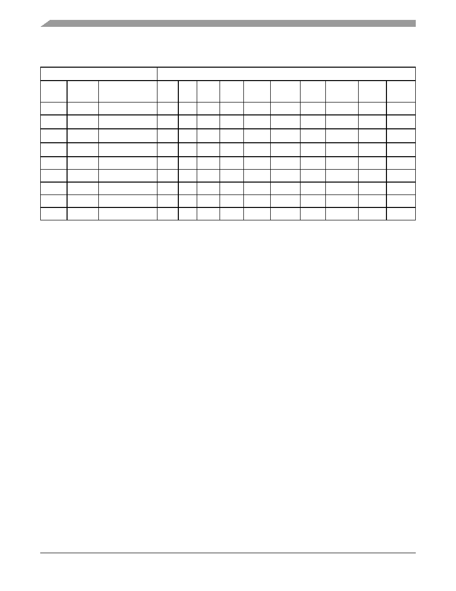
Table 2-2 56F8013 Pins
Peripherals:
LQFP
Pin #
Pin
Name
Signal Name
GPIO I2C
SCI
SPI
ADC
PWM
Quad
Timer
Power &
Ground
JTAG
Misc
1
GPIOB6
GPIOB6, RXD,
SDA, CLKIN
B6
SDA RXD
CLKIN
2
GPIOB1
GPIOB1, SS,
SDA
B1
SDA
SS
3
GPIOB7
GPIOB7, TXD,
SCL
B7
SCL
TXD
4
GPIOB5
GPIOB5, T1,
FAULT3
B5
FAULT3
T1
5
ANB0
ANB0, GPIOC4
C4
ANB0
6
ANB1
ANB1, GPIOC5
C5
ANB1
7
ANB2
ANB2, V
REFL
,
GPIOC6
C6
ANB2,
V
REFL
8
VDDA
V
DDA
V
DDA
9
VSSA
V
SSA
V
SSA
10
ANA2
ANA2, V
REFH
,
GPIOC2
C2
ANA2,
V
REFH
11
ANA1
ANA1, GPIOC1
C1
ANA1
12
ANA0
ANA0, GPIOC0
C0
ANA0
13
VSS_IO
V
SS_IO
V
SS_IO
14
TCK
TCK, GPIOD2
D2
TCK
15
RESET
RESET, GPIOA7
A7
RESET
16
GPIOB3
GPIOB3, MOSI,
T3
B3
MOSI
T3
17
GPIOB2
GPIOB2, MISO,
T2
B2
MISO
T2
18
GPIOA6
GPIOA6, FAULT0
A6
FAULT0
19
GPIOB4
GPIOB4, T0,
CLKO
B4
T0
CLKO
20
GPIOA5
GPIOA5, PWM5,
FAULT2, T3
A5
PWM5,
FAULT2
T3
21
GPIOB0
GPIOB0, SCLK,
SCL
B0
SCL
SCLK
22
GPIOA4
GPIOA4, PWM4,
FAULT1, T2
A4
PWM4,
FAULT1
T2
23
GPIOA2
GPIOA2, PWM2
A2
PWM2
56F8013 Technical Data, Rev. 2
14
Freescale Semiconductor
Preliminary
24
GPIOA3
GPIOA3, PWM3
A3
PWM3
25
VCAP
V
CAP
V
CAP
26
VDD_IO
V
DD_IO
V
DD_IO
27
VSS_IO
V
SS_IO
V
SS_IO
28
GPIOA1
GPIOA1, PWM1
A1
PWM1
29
GPIOA0
GPIOA0, PWM0
A0
PWM0
30
TDI
TDI, GPIOD0
D0
TDI
31
TMS
TMS, GPIOD3
D3
TMS
32
TDO
TDO, GPIOD1
D1
TDO
Table 2-2 56F8013 Pins (Continued)
Peripherals:
LQFP
Pin #
Pin
Name
Signal Name
GPIO I2C
SCI
SPI
ADC
PWM
Quad
Timer
Power &
Ground
JTAG
Misc

Introduction
56F8013 Technical Data, Rev. 2
Freescale Semiconductor
15
Preliminary
Figure 2-1 56F8013 Signals Identified by Functional Group (32-Pin LQFP)
V
DD_IO
V
DDA
V
SSA
GPIOB6 (RXD, SDA, CLKIN)
GPIOB7 (TXD, SCL)
Other
Supply
Ports
SCI Port or
I
2
C Port or
GPIO
JTAG/
EOnCE Port
or GPIO
1
1
2
V
CAP
1
1
1
TCK (GPIOD2)
TMS (GPIOD3)
GPIOA4 (PWM4, FAULT1, T2)
ANA0 - 1 (GPIOC0 - 1)
1
1
1
2
1
56F8013
1
TDI (GPIOD0)
TDO (GPIOD1)
GPIOB0 (SCLK, SCL)
GPIOB1 (SS, SDA)
GPIOB2 (MISO, T2)
GPIOB3 (MOSI, T3)
ANB0 - 1 (GPIOC4 - 5)
ANB2 (V
REFL
, GPIOC6)
1
1
1
1
1
1
1
2
ANA2 (V
REFH
, GPIOC2)
1
V
SS_IO
Power
Ground
Power
Ground
GPIOA3 (PWM3)
1
GPIOA0 - 2 (PWM0 - 2)
3
GPIOA5 (PWM5, FAULT2, T3)
1
GPIOA6 (FAULT0)
1
RESET
RESET ( GPIOA7)
1
GPIOB4 (T0, CLKO)
GPIOB5 (T1, FAULT3)
Timer Port
or GPIO
1
1
ADC Port or
GPIO
SPI Port or
I
2
C Port or
Timer Port
or GPIO
PWM Port or
Timer Port or
GPIO

56F8013 Technical Data, Rev. 2
16
Freescale Semiconductor
Preliminary
2.2 56F8013 Signal Pins
After reset, each pin is configured for its primary function (listed first). Any alternate functionality must
be programmed.
Table 2-3 56F8013 Signal and Package Information for the 32-Pin LQFP
Signal
Name
LQFP
Pin No.
Type
State During
Reset
Signal Description
V
DD_IO
26
Supply
Supply
I/O Power -- This pin supplies 3.3V power to the chip I/O interface.
V
SS_IO
13
Supply
Supply
V
SS
-- These pins provide ground for chip logic and I/O drivers.
V
SS_IO
27
V
DDA
8
Supply
Supply
ADC Power -- This pin supplies 3.3V power to the ADC modules. It
must be connected to a clean analog power supply.
V
SSA
9
Supply
Supply
ADC Analog Ground -- This pin supplies an analog ground to the
ADC modules.
V
CAP
25
Supply
Supply
V
CAP
-- Connect this pin to a 4.4
µ
F or greater bypass capacitor in
order to bypass the core voltage regulator, required for proper chip
operation. See
Section 10.2.1
.
GPIOB6
(RXD)
(SDA
1
)
(CLKIN)
1
Input/
Output
Input
Input/
Output
Input
Input, pulled
high
internally
Port B GPIO -- This GPIO pin can be individually programmed as
an input or output pin.
Receive Data -- SCI receive data input.
Serial Data -- This pin serves as the I
2
C serial data line.
Clock Input -- This pin serves as an optional external clock input.
After reset, the default state is GPIOB6. The peripheral functionality
is controlled via the SIM (See
Section 6.3.8
) and the CLKMODE bit
of the OCCS Oscillator Control Register.
1.
This signal is also brought out on the GPIOB1 pin.
Return to
Table 2-2

56F8013 Signal Pins
56F8013 Technical Data, Rev. 2
Freescale Semiconductor
17
Preliminary
GPIOB7
(TXD)
(SCL
2
)
3
Input/
Output
Input/
Output
Input/
Output
Input, pulled
high
internally
Port B GPIO -- This GPIO pin can be individually programmed as
an input or output pin.
Transmit Data -- SCI transmit data output or transmit / receive in
single wire operation.
Serial Clock -- This pin serves as the I
2
C serial clock.
After reset, the default state is GPIOB7. The peripheral functionality
is controlled via the SIM. See
Section 6.3.8
.
2.
This signal is also brought out on the GPIOB0 pin.
RESET
(GPIOA7)
15
Input
Input/Open
Drain
Output
Input, pulled
high
internally
Reset -- This input is a direct hardware reset on the processor.
When RESET is asserted low, the chip is initialized and placed in the
reset state. A Schmitt trigger input is used for noise immunity. The
internal reset signal will be deasserted synchronous with the internal
clocks after a fixed number of internal clocks.
Port A GPIO -- This GPIO pin can be individually programmed as
an input or open drain output pin. Note that RESET functionality is
disabled in this mode and the chip can only be reset via POR, COP
reset, or software reset.
After reset, the default state is RESET.
GPIOB4
(T0)
(CLKO)
19
Input/
Output
Input/
Output
Output
Input, pulled
high
internally
Port B GPIO -- This GPIO pin can be individually programmed as
an input or output pin.
T0 -- Timer, Channel 0
Clock Output -- This is a buffered clock signal. Using the
SIM_CLKO Select Register (SIM_CLKOSR), this pin can be
programmed as any of the following: disabled (logic 0), CLK_MSTR
(system clock), IPBus clock, or oscillator output. See
Section 6.3.7
.
After reset, the default state is GPIOB4. The peripheral functionality
is controlled via the SIM. See
Section 6.3.8
.
Return to
Table 2-2
Table 2-3 56F8013 Signal and Package Information for the 32-Pin LQFP (Continued)
Signal
Name
LQFP
Pin No.
Type
State During
Reset
Signal Description

56F8013 Technical Data, Rev. 2
18
Freescale Semiconductor
Preliminary
GPIOB5
(T1)
(FAULT3)
4
Input/
Output
Input/
Output
Output
Input, pulled
high
internally
Port B GPIO -- This GPIO pin can be individually programmed as
an input or output pin.
T1 -- Timer, Channel 1
FAULT3 -- This fault input pin is used for disabling selected PWM
outputs in cases where fault conditions originate off-chip.
After reset, the default state is GPIOB5. The peripheral functionality
is controlled via the SIM. See
Section 6.3.8
.
TCK
(GPIOD2)
14
Input
Input/
Output
Input, pulled
high
internally
Test Clock Input -- This input pin provides a gated clock to
synchronize the test logic and shift serial data to the JTAG/EOnCE
port. The pin is connected internally to a pull-up resistor. A Schmitt
trigger input is used for noise immunity.
Port D GPIO -- This GPIO pin can be individually programmed as
an input or output pin.
After reset, the default state is TCK.
TMS
(GPIOD3)
31
Input
Input/
Output
Input, pulled
high
internally
Test Mode Select Input -- This input pin is used to sequence the
JTAG TAP controller's state machine. It is sampled on the rising
edge of TCK and has an on-chip pull-up resistor.
Port D GPIO -- This GPIO pin can be individually programmed as
an input or output pin.
After reset, the default state is TMS.
TDI
(GPIOD0)
30
Input
Input/
Output
Input, pulled
high
internally
Test Data Input -- This input pin provides a serial input data stream
to the JTAG/EOnCE port. It is sampled on the rising edge of TCK
and has an on-chip pull-up resistor.
Port D GPIO -- This GPIO pin can be individually programmed as
an input or output pin.
After reset, the default state is TDI.
Return to
Table 2-2
Table 2-3 56F8013 Signal and Package Information for the 32-Pin LQFP (Continued)
Signal
Name
LQFP
Pin No.
Type
State During
Reset
Signal Description

56F8013 Signal Pins
56F8013 Technical Data, Rev. 2
Freescale Semiconductor
19
Preliminary
TDO
(GPIOD1)
32
Output
Input/
Output
Tri-stated,
pulled high
internally
Test Data Output -- This tri-stateable output pin provides a serial
output data stream from the JTAG/EOnCE port. It is driven in the
shift-IR and shift-DR controller states, and changes on the falling
edge of TCK.
Port D GPIO -- This GPIO pin can be individually programmed as
an input or output pin.
After reset, the default state is TDO.
GPIOB0
(SCLK)
(SCL
3
)
21
Input/
Output
Input/
Output
Input/
Output
Input, pulled
high
internally
Port B GPIO -- This GPIO pin can be individually programmed as
an input or output pin.
SPI Serial Clock -- In the master mode, this pin serves as an
output, clocking slaved listeners. In slave mode, this pin serves as
the data clock input. A Schmitt trigger input is used for noise
immunity.
Serial Data -- This pin serves as the I
2
C serial clock.
After reset, the default state is GPIOB0. The peripheral functionality
is controlled via the SIM. See
Section 6.3.8
.
3.
This signal is also brought out on the GPIOB7 pin.
GPIOB1
(SS)
(SDA
4
)
2
Input/
Output
Input
Input/
Output
Input, pulled
high
internally
Port B GPIO -- This GPIO pin can be individually programmed as
an input or output pin.
SPI Slave Select -- SS is used in slave mode to indicate to the SPI
module that the current transfer is to be received.
Serial Clock -- This pin serves as the I
2
C serial data line.
After reset, the default state is GPIOB1. The peripheral functionality
is controlled via the SIM. See
Section 6.3.8
.
4.
This signal is also brought out on the GPIOB6 pin.
Return to
Table 2-2
Table 2-3 56F8013 Signal and Package Information for the 32-Pin LQFP (Continued)
Signal
Name
LQFP
Pin No.
Type
State During
Reset
Signal Description

56F8013 Technical Data, Rev. 2
20
Freescale Semiconductor
Preliminary
GPIOB2
(MISO)
(T2
5
)
17
Input/
Output
Input/
Output
Input/
Output
Input, pulled
high
internally
Port B GPIO -- This GPIO pin can be individually programmed as
an input or output pin.
SPI Master In/Slave Out -- This serial data pin is an input to a
master device and an output from a slave device. The MISO line of a
slave device is placed in the high-impedance state if the slave device
is not selected. The slave device places data on the MISO line a
half-cycle before the clock edge the master device uses to latch the
data.
T2 -- Timer, Channel 2
After reset, the default state is GPIOB2. The peripheral functionality
is controlled via the SIM. See
Section 6.3.8
.
5.
This signal is also brought out on the GPIOA4 pin.
GPIOB3
(MOSI)
(T3
6
)
16
Input/
Output
Input/
Output
Input/
Output
Input, pulled
high
internally
Port B GPIO -- This GPIO pin can be individually programmed as
an input or output pin.
SPI Master Out/Slave In-- This serial data pin is an output from a
master device and an input to a slave device. The master device
places data on the MOSI line a half-cycle before the clock edge the
slave device uses to latch the data.
T3 -- Timer, Channel 3
After reset, the default state is GPIOB3. The peripheral functionality
is controlled via the SIM. See
Section 6.3.8
.
6.
This signal is also brought out on the GPIOA5 pin.
GPIOA0
(PWM0)
29
Input/
Output
Output
Input, pulled
high
internally
Port A GPIO -- This GPIO pin can be individually programmed as
an input or output pin.
PWM0 -- This is one of the six PWM output pins.
After reset, the default state is GPIOA0.
Return to
Table 2-2
Table 2-3 56F8013 Signal and Package Information for the 32-Pin LQFP (Continued)
Signal
Name
LQFP
Pin No.
Type
State During
Reset
Signal Description

56F8013 Signal Pins
56F8013 Technical Data, Rev. 2
Freescale Semiconductor
21
Preliminary
GPIOA1
(PWM1)
28
Input/
Output
Output
Input, pulled
high
internally
Port A GPIO -- This GPIO pin can be individually programmed as
an input or output pin.
PWM1 -- This is one of the six PWM output pins.
After reset, the default state is GPIOA1.
GPIOA2
(PWM2)
23
Input/
Output
Output
Input, pulled
high
internally
Port A GPIO -- This GPIO pin can be individually programmed as
an input or output pin.
PWM2 -- This is one of the six PWM output pins.
After reset, the default state is GPIOA2.
GPIOA3
(PWM3)
24
Input/
Output
Output
Input, pulled
high
internally
Port A GPIO -- This GPIO pin can be individually programmed as
an input or output pin.
PWM3 -- This is one of the six PWM output pins.
After reset, the default state is GPIOA3.
GPIOA4
(PWM4)
(FAULT1)
(T2
7
)
22
Input/
Output
Output
Input
Input/
Output
Input, pulled
high
internally
Port A GPIO -- This GPIO pin can be individually programmed as
an input or output pin.
PWM4 -- This is one of the six PWM output pins.
Fault1 -- This fault input pin is used for disabling selected PWM
outputs in cases where fault conditions originate off-chip.
T2 -- Timer, Channel 2
After reset, the default state is GPIOA4. The peripheral functionality
is controlled via the SIM. See
Section 6.3.8
.
7.
This signal is also brought out on the GPIOB2 pin.
Return to
Table 2-2
Table 2-3 56F8013 Signal and Package Information for the 32-Pin LQFP (Continued)
Signal
Name
LQFP
Pin No.
Type
State During
Reset
Signal Description

56F8013 Technical Data, Rev. 2
22
Freescale Semiconductor
Preliminary
GPIOA5
(PWM5)
(FAULT2)
(T3
8
)
20
Input/
Output
Output
Input/
Output
Input/
Output
Input, pulled
high
internally
Port A GPIO -- This GPIO pin can be individually programmed as
an input or output pin.
PWM5 -- This is one of the six PWM output pins.
Fault2 -- This fault input pin is used for disabling selected PWM
outputs in cases where fault conditions originate off-chip.
T3 -- Timer, Channel 3
After reset, the default state is GPIOA5. The peripheral functionality
is controlled via the SIM. See
Section 6.3.8
.
8.
This signal is also brought out on the GPIOB3 pin.
GPIOA6
(FAULT0)
18
Input/
Output
Input
Input, pulled
high
internally
Port A GPIO -- This GPIO pin can be individually programmed as
an input or output pin.
Fault0 -- This fault input pin is used for disabling selected PWM
outputs in cases where fault conditions originate off-chip.
After reset, the default state is GPIOA6.
ANA0
(GPIOC0)
12
Input
Input/
Output
Analog
Input
ANA0 -- Analog input to ADC A, channel 0
Port C GPIO -- This GPIO pin can be individually programmed as
an input or output pin.
After reset, the default state is ANA0.
ANA1
(GPIOC1)
11
Input
Input/
Output
Analog
Input
ANA1 -- Analog input to ADC A, channel 1
Port C GPIO -- This GPIO pin can be individually programmed as
an input or output pin.
After reset, the default state is ANA1.
Return to
Table 2-2
Table 2-3 56F8013 Signal and Package Information for the 32-Pin LQFP (Continued)
Signal
Name
LQFP
Pin No.
Type
State During
Reset
Signal Description

56F8013 Signal Pins
56F8013 Technical Data, Rev. 2
Freescale Semiconductor
23
Preliminary
ANA2
(V
REFH
)
(GPIOC2)
10
Input
Input
Input/
Output
Analog
Input
ANA2 -- Analog input to ADC A, channel 2
V
REFH
-- Analog reference voltage high
Port C GPIO -- This GPIO pin can be individually programmed as
an input or output pin.
After reset, the default state is ANA2.
ANB0
(GPIOC4)
5
Input
Input/
Output
Analog
Input
ANB0 -- Analog input to ADC B, channel 0
Port C GPIO -- This GPIO pin can be individually programmed as
an input or output pin.
After reset, the default state is ANB0.
ANB1
(GPIOC5)
6
Input
Input/
Output
Analog
Input
ANB1 -- Analog input to ADC B, channel 1
Port C GPIO -- This GPIO pin can be individually programmed as
an input or output pin.
After reset, the default state is ANB1.
ANB2
(V
REFL
)
(GPIOC6)
7
Input
Input
Input/
Output
Analog
Input
ANB2 -- Analog input to ADC B, channel 2
V
REFL
-- Analog reference voltage low. This should normally be
connected to a low-noise V
SS
.
Port C GPIO -- This GPIO pin can be individually programmed as
an input or output pin.
After reset, the default state is ANB2.
Return to
Table 2-2
Table 2-3 56F8013 Signal and Package Information for the 32-Pin LQFP (Continued)
Signal
Name
LQFP
Pin No.
Type
State During
Reset
Signal Description

56F8013 Technical Data, Rev. 2
24
Freescale Semiconductor
Preliminary
Part 3 OCCS
3.1 Overview
This module provides the 2X system clock frequency to the System Integration Module (SIM), which uses
it to generate the various chip clocks. This module also produces the OSC_CLK signals plus the ADC
clock and high-speed peripheral clock.
The on-chip clock synthesis module allows product design using an internal relaxation oscillator to run
56F8000 family parts at user-selectable frequencies up to 32MHz.
3.2 Features
The On-Chip Clock Synthesis (OCCS) module interfaces to the oscillator and PLL. The OCCS module
features:
∑
Internal relaxation oscillator
∑
Ability to power down the internal relaxation oscillator
∑
Ability to put the internal relaxation oscillator into a standby mode
∑
3-bit postscaler provides control for the PLL output
∑
Ability to power down the internal PLL
∑
Provides 2X master clock frequency and
OSC_CLK
signals
∑
Provides 3X fast peripheral clock to PWM and Timer
∑
Safety shutdown feature is available in the event that the PLL reference clock disappears
∑
Can be driven from an external clock source
The clock generation module provides the programming interface for both the PLL and internal relaxation
oscillator.
3.3 Operating Modes
In 56F8000 family parts, either an internal oscillator or an external frequency source can be used to provide
a reference clock (SYS_CLK2) to the SIM.
The 2X system clock source output from the OCCS can be described by one of the following equations:
2X system frequency = oscillator frequency
2X system frequency = (oscillator frequency X 8) / (postscaler)
where:
postscaler = 1, 2, 4, 8, 16, or 32 PLL output divider
The SIM is responsible for further dividing these frequencies by two, which will insure a 50% duty cycle
in the system clock output.

Operating Modes
56F8013 Technical Data, Rev. 2
Freescale Semiconductor
25
Preliminary
The 56F8000 family parts' on-chip clock synthesis module has the following registers:
∑
Control Register (OCCS_CR)
∑
Divide-by Register (OCCS_DB)
∑
Status Register (OCCS_SR)
∑
Shutdown Register (OCCS_SHUTDN)
∑
Oscillator Control Register (OCCS_OCTRL)
For more information on these registers, please refer to the 56F8000 Peripheral Reference Manual.
3.3.1
External Clock Source
The recommended method of connecting an external clock is illustrated in
Figure 3-1
. The external clock
source is connected to GPIOB6 / RXD.
Figure 3-1 Connecting an External Clock Signal using GPIOB6 / RXD
56F8013
GPIOB6 / RXD
External Clock
56F8013 Technical Data, Rev. 2
26
Freescale Semiconductor
Preliminary
3.4 Block Diagram
Figure 3-2
provides a block diagram which shows how the 56F8013 creates its internal clock, using the
relaxation oscillator as an 8MHz clock reference for the PLL.
Figure 3-2 OCCS Block Diagram with Relaxation Oscillator
TRIM[9:0]
ROSB
ROPD
Relaxation
OSC
Bus Interface and
Control
Bus
Interface
GPIOB6 / RXD
PRECS
MUX
MUX
MU
X
MSTR_OSC
SYS_CLK_x2
source to the SIM
(64MHz max)
ZSRC
HS PERF CLK
(96MHz max)
Postscaler
(
˜
1, 2, 4, 8, 16, 32)
Postscaler
(
˜
1, 2, 4, 8, 16, 32)
˜
3
˜
2
PLL
X 24
Lock
Detector
Loss of
Reference
Clock
Detector
Loss of Reference Clock Interrupt
LCK
F
OU
T
/2
F
EEDBACK
PLLCOD
FOUT

Pin Descriptions
56F8013 Technical Data, Rev. 2
Freescale Semiconductor
27
Preliminary
3.5 Pin Descriptions
3.5.1
External Reference (GPIOB6 / RXD)
The relaxation oscillator is included on chip and the reset mode is to use this as the clock source for the
chip. The user then has the option of switching to an external clock reference if desired.
Part 4 Memory Map
4.1 Introduction
The 56F8013 device is a 16-bit motor-control chip based on the 56800E core. It uses a Harvard-style
architecture with two independent memory spaces for Data and Program. On-chip RAM is used in both
spaces and Flash memory is used only in Program space.
This section provides memory maps for:
∑
Program Address Space, including the Interrupt Vector Table
∑
Data Address Space, including the EOnCE Memory and Peripheral Memory Maps
On-chip memory sizes for the device are summarized in
Table 4-1
. Flash memories' restrictions are
identified in the "Use Restrictions" column of
Table 4-1
.
4.2 Interrupt Vector Table
Table 4-2
provides the 56F8013's reset and interrupt priority structure, including on-chip peripherals. The
table is organized with higher-priority vectors at the top and lower-priority interrupts lower in the table.
As indicated, the priority of an interrupt can be assigned to different levels, allowing some control over
interrupt priorities. All level 3 interrupts will be serviced before level 2, and so on. For a selected priority
level, the lowest vector number has the highest priority.
The location of the vector table is determined by the Vector Base Address (VBA). Please see
Section
5.6.11
for the reset value of the VBA.
By default, VBA = 0, and the reset address and COP reset address will correspond to vector 0 and 1 of the
interrupt vector table. In these instances, the first two locations in the vector table must contain branch or
JMP instructions. All other entries must contain JSR instructions.
Table 4-1 Chip Memory Configurations
On-Chip Memory
56F8013
Use Restrictions
Program Flash
(PFLASH)
8k x 16
Erase / Program via Flash interface unit and word writes to CDBW
Unified RAM (ram)
2k x 16
Usable by both the Program and Data memory spaces

56F8013 Technical Data, Rev. 2
28
Freescale Semiconductor
Preliminary
Table 4-2 Interrupt Vector Table Contents
1
Peripheral
Vector
Number
Priority
Level
Vector Base
Address +
Interrupt Function
core
P:$00
Reserved for Reset Overlay
2
core
P:$02
Reserved for COP Reset Overlay
core
2
3
P:$04
Illegal Instruction
core
3
3
P:$06
SW Interrupt 3
core
4
3
P:$08
HW Stack Overflow
core
5
3
P:$0A
Misaligned Long Word Access
core
6
1-3
P:$0C
EOnCE Step Counter
core
7
1-3
P:$0E
EOnCE Breakpoint Unit 0
core
8
1-3
P:$10
EOnCE
Trace Buffer
core
9
1-3
P:$12
EOnCE Transmit Register Empty
core
10
1-3
P:$14
EOnCE Receive Register Full
core
11
2
P:$16
SW Interrupt 2
core
12
1
P:$18
SW Interrupt 1
core
13
0
P:$1A
SW Interrupt 0
14
Reserved
15
Reserved
PS
16
0-2
P:$20
Power Sense
OCCS
17
0-2
P:$22
PLL Lock, Loss of Clock Reference Interrupt
FM
18
0-2
P:$24
FM Access Error Interrupt
FM
19
0-2
P:$26
FM Command Complete
FM
20
0-2
P:$28
FM Command, data and address Buffers Empty
21
Reserved
GPIOD
22
0-2
P:$2C
GPIOD
GPIOC
23
0-2
P:$2E
GPIOC
GPIOB
24
0-2
P:$30
GPIOB
GPIOA
25
0-2
P:$32
GPIOA
SPI
26
0-2
P:$34
SPI Receiver Full / Error
SPI
27
0-2
P:$36
SPI Transmitter Empty
SCI
28
0-2
P:$38
SCI Transmitter Empty
SCI
29
0-2
P:$3A
SCI Transmitter Idle
SCI
30
0-2
P:$3C
SCI Reserved
SCI
31
0-2
P:$3E
SCI Receiver Error
SCI
32
0-2
P:$40
SCI Receiver Full
33, 34
Reserved
I
2
C
35
0-2
P:$46
I
2
C
Timer
36
0-2
P:$48
Timer Channel 0
Timer
37
0-2
P:$4A
Timer Channel 1
(Continues next page)

Program Map
56F8013 Technical Data, Rev. 2
Freescale Semiconductor
29
Preliminary
4.3 Program Map
The Program Memory map is shown in
Table 4-3
.
Timer
38
0-2
P:$4C
Timer Channel 2
Timer
39
0-2
P:$4E
Timer Channel 3
ADC
40
0-2
P:$50
ADCA Conversion Complete
ADC
41
0-2
P:$52
ADCB Conversion Complete
ADC
42
0-2
P:$54
ADC Zero Crossing or Limit Error
PWM
43
0-2
P:$56
Reload PWM
PWM
44
0-2
P:$58
PWM Fault
SWILP
45
-1
P:$5A
SW Interrupt Low Priority
1. Two words are allocated for each entry in the vector table. This does not allow the full address range to be referenced
from the vector table, providing only 19 bits of address.
2. If the VBA is set to $0000, the first two locations of the vector table will overlay the chip reset addresses.
Table 4-3 Program Memory Map
1
1. All addresses are 16-bit Word addresses.
Begin/End Address
Memory Allocation
P: $FF FFFF
P: $00 8800
RESERVED
P: $00 87FF
P: $00 8000
On-Chip RAM
2
4KB
2. This RAM is shared with Data space starting at address X: $00 0000;
see
Figure 4-1
.
P: $00 7FFF
P: $00 2000
RESERVED
P: $00 1FFF
P: $00 0000
Internal Program Flash
16KB
Cop Reset Address = $00 0002
Boot Location = $00 0000
Table 4-2 Interrupt Vector Table Contents
1
(Continued)
Peripheral
Vector
Number
Priority
Level
Vector Base
Address +
Interrupt Function

56F8013 Technical Data, Rev. 2
30
Freescale Semiconductor
Preliminary
4.4 Data Map
Figure 4-1 Dual Port RAM
Table 4-4 Data Memory Map
1
1. All addresses are 16-bit Word addresses.
Begin/End Address
Memory Allocation
X:$FF FFFF
X:$FF FF00
EOnCE
256 locations allocated
X:$FF FEFF
X:$01 0000
RESERVED
X:$00 FFFF
X:$00 F000
On-Chip Peripherals
4096 locations allocated
X:$00 EFFF
X:$00 8800
RESERVED
X:$00 EFFF
X:$00 0800
RESERVED
X:$00 7FFF
X:$00 0040
RESERVED
X:$00 07FF
X:$00 0000
On-Chip Data RAM
2
4KB
2. This RAM is shared with Program space starting at P: $00 8000; see
Figure 4-1
.
Reserved
RAM
Reserved
Flash
Reserved
EOnCE
Peripherals
Reserved
RAM
Dual Port RAM
Program
Data

EOnCE Memory Map
56F8013 Technical Data, Rev. 2
Freescale Semiconductor
31
Preliminary
4.5 EOnCE Memory Map
Figure 4-5
lists all EOnCE registers necessary to access or control the EOnCE.
Table 4-5 EOnCE Memory Map
Address
Register Acronym
Register Name
X:$FF FFFF
OTX1 / ORX1
Transmit Register Upper Word
Receive Register Upper Word
X:$FF FFFE
OTX / ORX (32 bits)
Transmit Register
Receive Register
X:$FF FFFD
OTXRXSR
Transmit and Receive Status and Control Register
X:$FF FFFC
OCLSR
Core Lock / Unlock Status Register
X:$FF FFFB - X:$FF FFA1
Reserved
X:$FF FFA0
OCR
Control Register
X:$FF FF9F
Instruction Step Counter
X:$FF FF9E
OSCNTR (24 bits)
Instruction Step Counter
X:$FF FF9D
OSR
Status Register
X:$FF FF9C
OBASE
Peripheral Base Address Register
X:$FF FF9B
OTBCR
Trace Buffer Control Register
X:$FF FF9A
OTBPR
Trace Buffer Pointer Register
X:$FF FF99
Trace Buffer Register Stages
X:$FF FF98
OTB (21 - 24 bits/stage) Trace Buffer Register Stages
X:$FF FF97
Breakpoint Unit Control Register
X:$FF FF96
OBCR (24 bits)
Breakpoint Unit Control Register
X:$FF FF95
Breakpoint Unit Address Register 1
X:$FF FF94
OBAR1 (24 bits)
Breakpoint Unit Address Register 1
X:$FF FF93
Breakpoint Unit Address Register 2
X:$FF FF92
OBAR2 (32 bits)
Breakpoint Unit Address Register 2
X:$FF FF91
Breakpoint Unit Mask Register 2
X:$FF FF90
OBMSK (32 bits)
Breakpoint Unit Mask Register 2
X:$FF FF8F
Reserved
X:$FF FF8E
OBCNTR
EOnCE Breakpoint Unit Counter
X:$FF FF8D
Reserved
X:$FF FF8C
Reserved
X:$FF FF8B
Reserved
X:$FF FF8A
OESCR
External Signal Control Register
X:$FF FF89 - X:$FF FF00
Reserved

56F8013 Technical Data, Rev. 2
32
Freescale Semiconductor
Preliminary
4.6 Peripheral Memory Mapped Registers
On-chip peripheral registers are part of the data memory map on the 56800E series. These locations may
be accessed with the same addressing modes used for ordinary Data memory, except all peripheral
registers should be read/written using word accesses only.
Table 4-6
summarizes base addresses for the set of peripherals on the 56F8013 device. Peripherals are
listed in order of the base address.
The following tables list all of the peripheral registers required to control or access the peripherals.
Table 4-6 Data Memory Peripheral Base Address Map Summary
Peripheral
Prefix
Base Address
Table Number
Timer TMRn
X:$00 F000
4-7
PWM
PWM
X:$00 F040
4-8
ITCN
ITCN
X:$00 F060
4-9
ADC
ADC
X:$00 F080
4-10
SCI SCI
X:$00
F0B0
4-11
SPI
SPI
X:$00 F0C0
4-12
I
2
C
I2C
X:$00 F0D0
4-13
COP
COP
X:$00 F0E0
4-14
CLK, PLL, OSC, TEST
OCCS
X:$00 F0F0
4-15
GPIO Port A
GPIOA
X:$00 F100
4-16
GPIO Port B
GPIOB
X:$00 F110
4-17
GPIO Port C
GPIOC
X:$00 F120
4-18
GPIO Port D
GPIOD
X:$00 F130
4-19
SIM
SIM
X:$00 F140
4-20
Power Supervisor
PS
X:$00 F160
4-21
FM
FM
X:$00 F400
4-22

Peripheral Memory Mapped Registers
56F8013 Technical Data, Rev. 2
Freescale Semiconductor
33
Preliminary
Table 4-7 Quad Timer Registers Address Map
(TMR_BASE = $00 F000)
Register Acronym
Address Offset
Register Description
TMR0_COMP1
$0
Compare Register 1
TMR0_COMP2
$1
Compare Register 2
TMR0_CAPT
$2
Capture Register
TMR0_LOAD
$3
Load Register
TMR0_HOLD
$4
Hold Register
TMR0_CNTR
$5
Counter Register
TMR0_CTRL
$6
Control Register
TMR0_SCTRL
$7
Status and Control Register
TMR0_CMPLD1
$8
Comparator Load Register 1
TMR0_CMPLD2
$9
Comparator Load Register 2
TMR0_CSCTRL
$A
Comparator Status and Control Register
Reserved
TMR1_COMP1
$10
Compare Register 1
TMR1_COMP2
$11
Compare Register 2
TMR1_CAPT
$12
Capture Register
TMR1_LOAD
$13
Load Register
TMR1_HOLD
$14
Hold Register
TMR1_CNTR
$15
Counter Register
TMR1_CTRL
$16
Control Register
TMR1_SCTRL
$17
Status and Control Register
TMR1_CMPLD1
$18
Comparator Load Register 1
TMR1_CMPLD2
$19
Comparator Load Register 2
TMR1_CSCTRL
$1A
Comparator Status and Control Register
Reserved
TMR2_COMP1
$20
Compare Register 1
TMR2_COMP2
$21
Compare Register 2
TMR2_CAPT
$22
Capture Register
TMR2_LOAD
$23
Load Register
TMR2_HOLD
$24
Hold Register
TMR2_CNTR
$25
Counter Register
TMR2_CTRL
$26
Control Register
TMR2_SCTRL
$27
Status and Control Register
TMR2_CMPLD1
$28
Comparator Load Register 1
TMR2_CMPLD2
$29
Comparator Load Register 2
TMR2_CSCTRL
$2A
Comparator Status and Control Register

56F8013 Technical Data, Rev. 2
34
Freescale Semiconductor
Preliminary
Reserved
TMR3_COMP1
$30
Compare Register 1
TMR3_COMP2
$31
Compare Register 2
TMR3_CAPT
$32
Capture Register
TMR3_LOAD
$33
Load Register
TMR3_HOLD
$34
Hold Register
TMR3_CNTR
$35
Counter Register
TMR3_CTRL
$36
Control Register
TMR3_SCTRL
$37
Status and Control Register
TMR3_CMPLD1
$38
Comparator Load Register 1
TMR3_CMPLD2
$39
Comparator Load Register 2
TMR3_CSCTRL
$3A
Comparator Status and Control Register
Table 4-8 Pulse Width Modulator Registers Address Map
(PWM_BASE = $00 F040)
Register Acronym
Address Offset
Register Description
PWM_CTRL
$0
Control Register
PWM_FCTRL
$1
Fault Control Register
PWM_FLTACK
$2
Fault Status Acknowledge Register
PWM_OUT
$3
Output Control Register
PWM_CNTR
$4
Counter Register
PWM_CMOD
$5
Counter Modulo Register
PWM_VAL0
$6
Value Register 0
PWM_VAL1
$7
Value Register 1
PWM_VAL2
$8
Value Register 2
PWM_VAL3
$9
Value Register 3
PWM_VAL4
$A
Value Register 4
PWM_VAL5
$B
Value Register 5
PWM_DTIM0
$C
Dead Time Register 0
PWM_DTIM1
$D
Dead Time Register 1
PWM_DMAP1
$E
Disable Mapping Register 1
PWM_DMAP2
$F
Disable Mapping Register 2
PWM_CNFG
$10
Configure Register
PWM_CCTRL
$11
Channel Control Register
PWM_PORT
$12
Port Register
PWM_ICCTRL
$13
Internal Correction Control Register
PWM_SCTRL
$14
Source Control Register
Table 4-7 Quad Timer Registers Address Map
(TMR_BASE = $00 F000) (Continued)
Register Acronym
Address Offset
Register Description
Peripheral Memory Mapped Registers
56F8013 Technical Data, Rev. 2
Freescale Semiconductor
35
Preliminary
Table 4-9 Interrupt Control Registers Address Map
(ITCN_BASE = $00 F060)
Register Acronym
Address Offset
Register Description
ITCN_IPR0
$0
Interrupt Priority Register 0
ITCN_IPR1
$1
Interrupt Priority Register 1
ITCN_IPR2
$2
Interrupt Priority Register 2
ITCN_IPR3
$3
Interrupt Priority Register 3
ITCN_IPR4
$4
Interrupt Priority Register 4
ITCN_VBA
$5
Vector Base Address Register
ITCN_FIM0
$6
Fast Interrupt Match 0 Register
ITCN_FIVAL0
$7
Fast Interrupt Vector Address Low 0 Register
ITCN_FIVAH0
$8
Fast Interrupt Vector Address High 0 Register
ITCN_FIM1
$9
Fast Interrupt Match 1 Register
ITCN_FIVAL1
$A
Fast Interrupt Vector Address Low 1 Register
ITCN_FIVAH1
$B
Fast Interrupt Vector Address High 1 Register
ITCN_IRQP0
$C
IRQ Pending Register 0
ITCN_IRQP1
$D
IRQ Pending Register 1
ITCN_IRQP2
$E
IRQ Pending Register 2
Reserved
ITCN_ICTRL
$12
Interrupt Control Register
Reserved
Table 4-10 Analog-to-Digital Converter Registers Address Map
(ADC_BASE = $00 F080)
Register Acronym
Address Offset
Register Description
ADC_CTRL1
$0
Control Register 1
ADC_CTRL2
$1
Control Register 2
ADC_ZXCTRL
$2
Zero Crossing Control Register
ADC_CLIST 1
$3
Channel List Register 1
ADC_CLIST 2
$4
Channel List Register 2
ADC_SDIS
$5
Sample Disable Register
ADC_STAT
$6
Status Register
ADC_LIMSTAT
$7
Limit Status Register
ADC_ZXSTAT
$8
Zero Crossing Status Register
ADC_RSLT0
$9
Result Register 0
ADC_RSLT1
$A
Result Register 1
ADC_RSLT2
$B
Result Register 2

56F8013 Technical Data, Rev. 2
36
Freescale Semiconductor
Preliminary
ADC_RSLT3
$C
Result Register 3
ADC_RSLT4
$D
Result Register 4
ADC_RSLT5
$E
Result Register 5
ADC_RSLT6
$F
Result Register 6
ADC_RSLT7
$10
Result Register 7
ADC_LOLIM0
$11
Low Limit Register 0
ADC_LOLIM1
$12
Low Limit Register 1
ADC_LOLIM2
$13
Low Limit Register 2
ADC_LOLIM3
$14
Low Limit Register 3
ADC_LOLIM4
$15
Low Limit Register 4
ADC_LOLIM5
$16
Low Limit Register 5
ADC_LOLIM6
$17
Low Limit Register 6
ADC_LOLIM7
$18
Low Limit Register 7
ADC_HILIM0
$19
High Limit Register 0
ADC_HILIM1
$1A
High Limit Register 1
ADC_HILIM2
$1B
High Limit Register 2
ADC_HILIM3
$1C
High Limit Register 3
ADC_HILIM4
$1D
High Limit Register 4
ADC_HILIM5
$1E
High Limit Register 5
ADC_HILIM6
$1F
High Limit Register 6
ADC_HILIM7
$20
High Limit Register 7
ADC_OFFST0
$21
Offset Register 0
ADC_OFFST1
$22
Offset Register 1
ADC_OFFST2
$23
Offset Register 2
ADC_OFFST3
$24
Offset Register 3
ADC_OFFST4
$25
Offset Register 4
ADC_OFFST5
$26
Offset Register 5
ADC_OFFST6
$27
Offset Register 6
ADC_OFFST7
$28
Offset Register 7
ADC_PWR
$29
Power Control Register
ADC_VREF
$2A
Voltage Reference Register
Reserved
Table 4-10 Analog-to-Digital Converter Registers Address Map
(ADC_BASE = $00 F080) (Continued)
Register Acronym
Address Offset
Register Description

Peripheral Memory Mapped Registers
56F8013 Technical Data, Rev. 2
Freescale Semiconductor
37
Preliminary
Table 4-11 Serial Communication Interface Registers Address Map
(SCI_BASE = $00 F0B0)
Register Acronym
Address Offset
Register Description
SCI_RATE
$0
Baud Rate Register
SCI_CTRL1
$1
Control Register 1
SCI_CTRL2
$2
Control Register 2
SCI_STAT
$3
Status Register
SCI_DATA
$4
Data Register
Table 4-12 Serial Peripheral Interface Registers Address Map
(SPI_BASE = $00 F0C0)
Register Acronym
Address Offset
Register Description
SPI_SCTRL
$0
Status and Control Register
SPI_DSCTRL
$1
Data Size and ControlRegister
SPI_DRCV
$2
Data Receive Register
SPI_DXMIT
$3
Data Transmit Register
Table 4-13 I
2
C Registers Address Map
(I2C_BASE = $00 F0D0)
Register Acronym
Address Offset
Register Description
I2C_ADDR
$0
Address Register
I2C_FDIV
$1
Frequency Divider Register
I2C_CTRL
$2
Control Register
I2C_STAT
$3
Status Register
I2C_DATA
$4
Data I/O Register
I2C_NFILT
$5
Noise Filter Register
Table 4-14 Computer Operating Properly Registers Address Map
(COP_BASE = $00 F0E0)
Register Acronym
Address Offset
Register Description
COP_CTRL
$0
Control Register
COP_TOUT
$1
Time-Out Register
COP_CNTR
$2
Counter Register

56F8013 Technical Data, Rev. 2
38
Freescale Semiconductor
Preliminary
Table 4-15 Clock Generation Module Registers Address Map
(OCCS_BASE = $00 F0F0)
Register Acronym
Address Offset
Register Description
OCCS_CTRL
$0
Control Register
OCCS_DIVBY
$1
Divide-By Register
OCCS_STAT
$2
Status Register
Reserved
OCCS_SHUTDN
$4
Shutdown Register
OCCS_OCTRL
$5
Oscillator Control Register
Table 4-16 GPIOA Registers Address Map
(GPIOA_BASE = $00 F100)
Register Acronym
Address Offset
Register Description
GPIOA_PUPEN
$0
Pull-up Enable Register
GPIOA_DATA
$1
Data Register
GPIOA_DDIR
$2
Data Direction Register
GPIOA_PEREN
$3
Peripheral Enable Register
GPIOA_IASSRT
$4
Interrupt Assert Register
GPIOA_IEN
$5
Interrupt Enable Register
GPIOA_IEPOL
$6
Interrupt Edge Polarity Register
GPIOA_IPEND
$7
Interrupt Pending Register
GPIOA_IEDGE
$8
Interrupt Edge-Sensitive Register
GPIOA_PPOUTM
$9
Push-Pull Output Mode Control Register
GPIOA_RDATA
$A
Raw Data Register
GPIOA_DRIVE
$B
Drive Strength Control Register

Peripheral Memory Mapped Registers
56F8013 Technical Data, Rev. 2
Freescale Semiconductor
39
Preliminary
Table 4-17 GPIOB Registers Address Map
(GPIOB_BASE = $00 F110)
Register Acronym
Address Offset
Register Description
GPIOB_PUPEN
$0
Pull-up Enable Register
GPIOB_DATA
$1
Data Register
GPIOB_DDIR
$2
Data Direction Register
GPIOB_PEREN
$3
Peripheral Enable Register
GPIOB_IASSRT
$4
Interrupt Assert Register
GPIOB_IEN
$5
Interrupt Enable Register
GPIOB_IEPOL
$6
Interrupt Edge Polarity Register
GPIOB_IPEND
$7
Interrupt Pending Register
GPIOB_IEDGE
$8
Interrupt Edge-Sensitive Register
GPIOB_PPOUTM
$9
Push-Pull Output Mode Control Register
GPIOB_RDATA
$A
Raw Data Register
GPIOB_DRIVE
$B
Drive Strength Control Register
Table 4-18 GPIOC Registers Address Map
(GPIOC_BASE = $00 F120)
Register Acronym
Address Offset
Register Description
GPIOC_PUPEN
$0
Pull-up Enable Register
GPIOC_DATA
$1
Data Register
GPIOC_DDIR
$2
Data Direction Register
GPIOC_PEREN
$3
Peripheral Enable Register
GPIOC_IASSRT
$4
Interrupt Assert Register
GPIOC_IEN
$5
Interrupt Enable Register
GPIOC_IEPOL
$6
Interrupt Edge Polarity Register
GPIOC_IPEND
$7
Interrupt Pending Register
GPIOC_IEDGE
$8
Interrupt Edge-Sensitive Register
GPIOC_PPOUTM
$9
Push-Pull Output Mode Control Register
GPIOC_RDATA
$A
Raw Data Register
GPIOC_DRIVE
$B
Drive Strength Control Register

56F8013 Technical Data, Rev. 2
40
Freescale Semiconductor
Preliminary
Table 4-19 GPIOD Registers Address Map
(GPIOD_BASE = $00 F130)
Register Acronym
Address Offset
Register Description
GPIOD_PUPEN
$0
Pull-up Enable Register
GPIOD_DATA
$1
Data Register
GPIOD_DDIR
$2
Data Direction Register
GPIOD_PEREN
$3
Peripheral Enable Register
GPIOD_IASSRT
$4
Interrupt Assert Register
GPIOD_IEN
$5
Interrupt Enable Register
GPIOD_IEPOL
$6
Interrupt Edge Polarity Register
GPIOD_IPEND
$7
Interrupt Pending Register
GPIOD_IEDGE
$8
Interrupt Edge-Sensitive Register
GPIOD_PPOUTM
$9
Push-Pull Output Mode Control Register
GPIOD_RDATA
$A
Raw Data Register
GPIOD_DRIVE
$B
Drive Strength Control Register
Table 4-20 System Integration Module Registers Address Map
(SIM_BASE = $00 F140)
Register Acronym
Address Offset
Register Description
SIM_CTRL
$0
Control Register
SIM_RSTAT
$1
Reset Status Register
SIM_SWC0
$2
Software Control Register 0
SIM_SWC1
$3
Software Control Register 1
SIM_SWC2
$4
Software Control Register 2
SIM_SWC3
$5
Software Control Register 3
SIM_MSHID
$6
Most Significant Half JTAG ID
SIM_LSHID
$7
Least Significant Half JTAG ID
SIM_PWR
$8
Power Control Register
Reserved
SIM_CLKOUT
$A
Clock Out Select Register
SIM_GPS
$B
GPIO Peripheral Select Register
SIM_PCE
$C
Peripheral Clock Enable Register
SIM_IOSAHI
$D
I/O Short Address Location High Register
SIM_IOSALO
$E
I/O Short Address Location Low Register

Peripheral Memory Mapped Registers
56F8013 Technical Data, Rev. 2
Freescale Semiconductor
41
Preliminary
Table 4-21 Power Supervisor Registers Address Map
(PS_BASE = $00 F160)
Register Acronym
Address Offset
Register Description
PS_CTRL
$0
Control Register
PS_STAT
$1
Status Register
Table 4-22 Flash Module Registers Address Map
(FM_BASE = $00 F400)
Register Acronym
Address Offset
Register Description
FM_CLKDIV
$0
Clock Divider Register
FM_CNFG
$1
Configuration Register
$2
Reserved
FM_SECHI
$3
Security High Half Register
FM_SECLO
$4
Security Low Half Register
$5 - $9
Reserved
FM_PROT
$10
Protection Register
$11 - $12
Reserved
FM_USTAT
$13
User Status Register
FM_CMD
$14
Command Register
$15
Reserved
$16
Reserved
$17
Reserved
FM_DATA
$18
Data Buffer Register
$19
Reserved
$1A
Reserved
FM_OPT1
$1B
Optional Data 1 Register
Reserved
FM_TSTSIG
$1D
Test Array Signature Register

56F8013 Technical Data, Rev. 2
42
Freescale Semiconductor
Preliminary
Part 5 Interrupt Controller (ITCN)
5.1 Introduction
The Interrupt Controller (ITCN) module is used to arbitrate between various interrupt requests (IRQs), to
signal to the 56800E core when an interrupt of sufficient priority exists, and to what address to jump in
order to service this interrupt.
5.2 Features
The ITCN module design includes these distinctive features:
∑
Programmable priority levels for each IRQ
∑
Two programmable Fast Interrupts
∑
Notification to SIM module to restart clocks out of Wait and Stop modes
∑
Ability to drive initial address on the address bus after reset
For further information, see
Table 4-2
, Interrupt Vector Table Contents.
5.3 Functional Description
The Interrupt Controller is a slave on the IPBus. It contains registers that allow each of the 46 interrupt
sources to be set to one of four priority levels (excluding certain interrupts that are of fixed priority). Next,
all of the interrupt requests of a given level are priority encoded to determine the lowest numerical value
of the active interrupt requests for that level. Within a given priority level, number 0 is the highest priority
and number 45 is the lowest.
5.3.1
Normal Interrupt Handling
Once the INTC has determined that an interrupt is to be serviced and which interrupt has the highest
priority, an interrupt vector address is generated. Normal interrupt handling concatenates the Vector Base
Address (VBA) and the vector number to determine the vector address, generating an offset into the vector
table for each interrupt.
Functional Description
56F8013 Technical Data, Rev. 2
Freescale Semiconductor
43
Preliminary
5.3.2
Interrupt Nesting
Interrupt exceptions may be nested to allow an IRQ of higher priority than the current exception to be
serviced. The following table defines the nesting requirements for each priority level.
5.3.3
Fast Interrupt Handling
Fast interrupts are described in the DSP56800E Reference Manual. The interrupt controller recognizes
Fast Interrupts before the core does.
A Fast Interrupt is defined (to the ITCN) by:
1. Setting the priority of the interrupt as level 2, with the appropriate field in the IPR registers
2. Setting the FIMn register to the appropriate vector number
3. Setting the FIVALn and FIVAHn registers with the address of the code for the
Fast Interrupt
When an interrupt occurs, its vector number is compared with the FIM0 and FIM1 register values. If a
match occurs, and it is a level 2 interrupt, the ITCN handles it as a Fast Interrupt. The ITCN takes the vector
address from the appropriate FIVALn and FIVAHn registers, instead of generating an address that is an
offset from the VBA.
The core then fetches the instruction from the indicated vector adddress and if it is not a JSR, the core starts
its Fast Interrupt handling.
Table 5-1 Interrupt Mask Bit Definition
SR[9]
SR[8]
Exceptions Permitted
Exceptions Masked
0
0
Priorities 0, 1, 2, 3
None
0
1
Priorities 1, 2, 3
Priority 0
1
0
Priorities 2, 3
Priorities 0, 1
1
1
Priority 3
Priorities 0, 1, 2

56F8013 Technical Data, Rev. 2
44
Freescale Semiconductor
Preliminary
5.4 Block Diagram
Figure 5-1 Interrupt Controller Block Diagram
5.5 Operating Modes
The ITCN module design contains two major modes of operation:
∑
Functional Mode
The ITCN is in this mode by default.
∑
Wait and Stop Modes
During Wait and Stop modes, the system clocks and the 56800E core are turned off. The ITCN will signal
a pending IRQ to the System Integration Module (SIM) to restart the clocks and service the IRQ. An IRQ
can only wake up the core if the IRQ is enabled prior to entering the Wait or Stop mode.
Priority
Level
2 -> 4
Decode
INT0
Priority
Level
2 -> 4
Decode
INT45
Level 0
46 -> 6
Priority
Encoder
any0
Level 3
46 -> 6
Priority
Encoder
any3
INT
VAB
IPIC
CONTROL
6
6
PIC_EN
IACK
SR[9:8]

Register Descriptions
56F8013 Technical Data, Rev. 2
Freescale Semiconductor
45
Preliminary
5.6 Register Descriptions
A register address is the sum of a base address and an address offset. The base address is defined at the
system level and the address offset is defined at the module level. The ITCN module has 16 registers.
Table 5-2 ITCN Register Summary
(ITCN_BASE = $00 F060)
Register
Acronym
Base Address +
Register Name
Section Location
IPR0
$0
Interrupt Priority Register 0
5.6.1
IPR1
$1
Interrupt Priority Register 1
5.6.2
IPR2
$2
Interrupt Priority Register 2
5.6.3
IPR3
$3
Interrupt Priority Register 3
5.6.4
IPR4
$4
Interrupt Priority Register 4
5.6.5
VBA
$5
Vector Base Address Register
5.6.6
FIM0
$6
Fast Interrupt Match 0 Register
5.6.7
FIVAL0
$7
Fast Interrupt 0 Vector Address Low Register
5.6.8
FIVAH0
$8
Fast Interrupt 0 Vector Address High 0 Register
5.6.9
FIM1
$9
Fast Interrupt Match 1 Register
5.6.10
FIVAL1
$A
Fast Interrupt 1 Vector Address Low Register
5.6.11
FIVAH1
$B
Fast Interrupt 1 Vector Address High Register
5.6.12
IRQP0
$C
IRQ Pending Register 0
5.6.13
IRQP1
$D
IRQ Pending Register 1
5.6.14
IRQP2
$E
IRQ Pending Register 2
5.6.15
Reserved
ICTRL
$12
Interrupt Control Register
5.6.16
Reserved

56F8013 Technical Data, Rev. 2
46
Freescale Semiconductor
Preliminary
Figure 5-2 ITCN Register Map Summary
Add.
Offset
Register
Name
15
14
13
12
11
10
9
8
7
6
5
4
3
2
1
0
$0
IPR0
R
LVI IPL
0
0
0
0
RX_REG IPL
TX_REG IPL
TRBUF IPL
BKPT_U IPL
STPCNT IPL
W
$1
IPR1
R
GPIOB IPL
GPIOC IPL
GPIOD IPL
0
0
FM_CBE IPL
FM_CC IPL
FM_ERR IPL
PLL IPL
W
$2
IPR2
R
SCI_RCV
IPL
SCI_RERR
IPL
0
0
SCI_TIDL IPL
SCI_XMIT
IPL
SPI_XMIT
IPL
SPI_RCV IPL
GPIOA IPL
W
$3
IPR3
R
ADCA_CC
IPL
TMR_3 IPL
TMR_2 IPL
TMR_1 IPL
TMR_0 IPL
I2C_ADDR
IPL
0
0
0
0
W
$4
IPR4
R
0
0
0
0
0
0
0
0
PWM_F IPL
PWM_RL IPL
ADC_ZC_LE
IPL
ADCB_CC IPL
W
$5
VBA
R
0
0
VECTOR_BASE_ADDRESS
W
$6
FIM0
R
0
0
0
0
0
0
0
0
0
0
FAST INTERRUPT 0
W
$7
FIVAL0
R
FAST INTERRUPT 0 VECTOR ADDRESS LOW
W
$8
FIVAH0
R
0
0
0
0
0
0
0
0
0
0
0
FAST INTERRUPT 0 VECTOR
ADDRESS HIGH
W
$9
FIM1
R
0
0
0
0
0
0
0
0
0
0
FAST INTERRUPT 1
W
$A
FIVAL1
R
FAST INTERRUPT 1 VECTOR ADDRESS LOW
W
$B
FIVAH1
R
0
0
0
0
0
0
0
0
0
0
0
FAST INTERRUPT 1 VECTOR
ADDRESS HIGH
W
$C
IRQP0
R
PENDING[16:2]
1
W
$D
IRQP1
R
PENDING[32:17]
W
$E
IRQP2
R
1
1
1
PENDING[45:33]
W
Reserved
$12
ICTRL
R
INT
IPIC
VAB
INT_
DIS
1
1
1
0
0
W
Reserved
= Reserved

Register Descriptions
56F8013 Technical Data, Rev. 2
Freescale Semiconductor
47
Preliminary
5.6.1
Interrupt Priority Register 0 (IPR0)
Figure 5-3 Interrupt Priority Register 0 (IPR0)
5.6.1.1 LVI IPL--Bits 15≠14
This field is used to set the interrupt priority levels for a peripheral IRQ. This IRQ is limited to priorities
0 through 2 and is disabled by default.
∑
00 = IRQ disabled (default)
∑
01 = IRQ is priority level 0
∑
10 = IRQ is priority level 1
∑
11 = IRQ is priority level 2
5.6.1.2 Reserved--Bits 13≠10
This bit field is reserved or not implemented. It is read as 0 and cannot be modified by writing.
5.6.1.3 EOnCE Receive Register Full Interrupt Priority Level
(RX_REG IPL)-- Bits 9≠8
This field is used to set the interrupt priority level for IRQs. This IRQ is limited to priorities 1 through 3.
It is disabled by default.
∑
00 = IRQ disabled (default)
∑
01 = IRQ is priority level 1
∑
10 = IRQ is priority level 2
∑
11 = IRQ is priority level 3
5.6.1.4 EOnCE Transmit Register Empty Interrupt Priority Level
(TX_REG IPL)-- Bits 7≠6
This field is used to set the interrupt priority level for IRQs. This IRQ is limited to priorities 1 through 3.
It is disabled by default.
∑
00 = IRQ disabled (default)
∑
01 = IRQ is priority level 1
∑
10 = IRQ is priority level 2
∑
11 = IRQ is priority level 3
Base + $0
15
14
13
12
11
10
9
8
7
6
5
4
3
2
1
0
Read
LVI IPL
0
0
0
0
RX_REG IPL
TX_REG IPL
TRBUF IPL
BKPT_U IPL
STPCNT IPL
Write
RESET
0
0
0
0
0
0
0
0
0
0
0
0
0
0
0
0

56F8013 Technical Data, Rev. 2
48
Freescale Semiconductor
Preliminary
5.6.1.5 EOnCE Trace Buffer Interrupt Priority Level
(TRBUF IPL)-- Bits 5≠4
This field is used to set the interrupt priority level for IRQs. This IRQ is limited to priorities 1 through 3.
It is disabled by default.
∑
00 = IRQ disabled (default)
∑
01 = IRQ is priority level 1
∑
10 = IRQ is priority level 2
∑
11 = IRQ is priority level 3
5.6.1.6 EOnCE Breakpoint Unit Interrupt Priority Level
(BKPT_U IPL)-- Bits 3≠2
This field is used to set the interrupt priority level for IRQs. This IRQ is limited to priorities 1 through 3.
It is disabled by default.
∑
00 = IRQ disabled (default)
∑
01 = IRQ is priority level 1
∑
10 = IRQ is priority level 2
∑
11 = IRQ is priority level 3
5.6.1.7 EOnCE Step Counter Interrupt Priority Level
(STPCNT IPL)-- Bits 1≠0
This field is used to set the interrupt priority level for IRQs. This IRQ is limited to priorities 1 through 3.
It is disabled by default.
∑
00 = IRQ disabled (default)
∑
01 = IRQ is priority level 1
∑
10 = IRQ is priority level 2
∑
11 = IRQ is priority level 3
5.6.2
Interrupt Priority Register 1 (IPR1)
Figure 5-4 Interrupt Priority Register 1 (IPR1)
Base + $1
15
14
13
12
11
10
9
8
7
6
5
4
3
2
1
0
Read
GPIOB IPL
GPIOC IPL
GPIOD IPL
0
0
FM_CBE IPL
FM_CC IPL
FM_ERR IPL
PLL IPL
Write
RESET
0
0
0
0
0
0
0
0
0
0
0
0
0
0
0
0

Register Descriptions
56F8013 Technical Data, Rev. 2
Freescale Semiconductor
49
Preliminary
5.6.2.1 GPIOB Interrupt Priority Level (GPIOB IPL)--Bits 15≠14
This field is used to set the interrupt priority level for IRQs. This IRQ is limited to priorities 0 through 2.
It is disabled by default.
∑
00 = IRQ disabled (default)
∑
01 = IRQ is priority level 0
∑
10 = IRQ is priority level 1
∑
11 = IRQ is priority level 2
5.6.2.2 GPIOC Interrupt Priority Level (GPIOC IPL)--Bits 13≠12
This field is used to set the interrupt priority level for IRQs. This IRQ is limited to priorities 0 through 2.
It is disabled by default.
∑
00 = IRQ disabled (default)
∑
01 = IRQ is priority level 0
∑
10 = IRQ is priority level 1
∑
11 = IRQ is priority level 2
5.6.2.3 GPIOD Interrupt Priority Level (GPIOD IPL)--Bits 11≠10
This field is used to set the interrupt priority level for IRQs. This IRQ is limited to priorities 0 through 2.
It is disabled by default.
∑
00 = IRQ disabled (default)
∑
01 = IRQ is priority level 0
∑
10 = IRQ is priority level 1
∑
11 = IRQ is priority level 2
5.6.2.4 Reserved--Bits 9≠8
This bit field is reserved or not implemented. It is read as 0 and cannot be modified by writing.
5.6.2.5 FM Command, Data, Address Buffers Empty Interrupt Priority Level
(FM_CBE IPL)--Bits 7≠6
This field is used to set the interrupt priority level for IRQs. This IRQ is limited to priorities 0 through 2.
It is disabled by default.
∑
00 = IRQ disabled (default)
∑
01 = IRQ is priority level 0
∑
10 = IRQ is priority level 1
∑
11 = IRQ is priority level 2
56F8013 Technical Data, Rev. 2
50
Freescale Semiconductor
Preliminary
5.6.2.6 FM Command Complete Priority Level (FM_CC IPL)--Bits 5≠4
This field is used to set the interrupt priority level for IRQs. This IRQ is limited to priorities 0 through 2.
It is disabled by default.
∑
00 = IRQ disabled (default)
∑
01 = IRQ is priority level 0
∑
10 = IRQ is priority level 1
∑
11 = IRQ is priority level 2
5.6.2.7 FM Error Interrupt Priority Level (FM_ERR IPL)--Bits 3≠2
This field is used to set the interrupt priority level for IRQs. This IRQ is limited to priorities 0 through 2.
It is disabled by default.
∑
00 = IRQ disabled (default)
∑
01 = IRQ is priority level 0
∑
10 = IRQ is priority level 1
∑
11 = IRQ is priority level 2
5.6.2.8 PLL Loss of Reference or Change in Lock Status Interrupt Priority Level
(PLL IPL)--Bits 1≠0
This field is used to set the interrupt priority level for IRQs. This IRQ is limited to priorities 0 through 2.
It is disabled by default.
∑
00 = IRQ disabled (default)
∑
01 = IRQ is priority level 0
∑
10 = IRQ is priority level 1
∑
11 = IRQ is priority level 2
5.6.3
Interrupt Priority Register 2 (IPR2)
Figure 5-5 Interrupt Priority Register 2 (IPR2)
Base + $2
15
14
13
12
11
10
9
8
7
6
5
4
3
2
1
0
Read
SCI_RCV IPL
SCI_RERR
IPL
0
0
SCI_TIDL IPL SCI_XMIT IPL SPI_XMIT IPL SPI_RCV IPL
GPIOA IPL
Write
RESET
0
0
0
0
0
0
0
0
0
0
0
0
0
0
0
0

Register Descriptions
56F8013 Technical Data, Rev. 2
Freescale Semiconductor
51
Preliminary
5.6.3.1 SCI Receiver Full Interrupt Priority Level (SCI_RCV IPL)--
Bits 15≠14
This field is used to set the interrupt priority level for IRQs. This IRQ is limited to priorities 0 through 2.
It is disabled by default.
∑
00 = IRQ disabled (default)
∑
01 = IRQ is priority level 0
∑
10 = IRQ is priority level 1
∑
11 = IRQ is priority level 2
5.6.3.2 SCI Receiver Error Interrupt Priority Level (SCI_RERR IPL)--
Bits 13≠12
This field is used to set the interrupt priority level for IRQs. This IRQ is limited to priorities 0 through 2.
It is disabled by default.
∑
00 = IRQ disabled (default)
∑
01 = IRQ is priority level 0
∑
10 = IRQ is priority level 1
∑
11 = IRQ is priority level 2
5.6.3.3 Reserved--Bits 11≠10
This bit field is reserved or not implemented. It is read as 0 and cannot be modified by writing.
5.6.3.4 SCI Transmitter Idle Interrupt Priority Level (SCI_TIDL IPL)--
Bits 9≠8
This field is used to set the interrupt priority level for IRQs. This IRQ is limited to priorities 0 through 2.
It is disabled by default.
∑
00 = IRQ disabled (default)
∑
01 = IRQ is priority level 0
∑
10 = IRQ is priority level 1
∑
11 = IRQ is priority level 2
5.6.3.5 SCI Transmitter Empty Interrupt Priority Level (SCI_XMIT IPL)--
Bits 7≠6
This field is used to set the interrupt priority level for IRQs. This IRQ is limited to priorities 0 through 2.
It is disabled by default.
∑
00 = IRQ disabled (default)
∑
01 = IRQ is priority level 0
∑
10 = IRQ is priority level 1
∑
11 = IRQ is priority level 2

56F8013 Technical Data, Rev. 2
52
Freescale Semiconductor
Preliminary
5.6.3.6 SPI Transmitter Empty Interrupt Priority Level (SPI_XMIT IPL)--
Bits 5≠4
This field is used to set the interrupt priority level for IRQs. This IRQ is limited to priorities 0 through 2.
It is disabled by default.
∑
00 = IRQ disabled (default)
∑
01 = IRQ is priority level 0
∑
10 = IRQ is priority level 1
∑
11 = IRQ is priority level 2
5.6.3.7 SPI Receiver Full Interrupt Priority Level (SPI_RCV IPL)--
Bits 3≠2
This field is used to set the interrupt priority level for IRQs. This IRQ is limited to priorities 0 through 2.
It is disabled by default.
∑
00 = IRQ disabled (default)
∑
01 = IRQ is priority level 0
∑
10 = IRQ is priority level 1
∑
11 = IRQ is priority level 2
5.6.3.8 GPIOA Interrupt Priority Level (GPIOA IPL)--Bits 1≠0
This field is used to set the interrupt priority level for IRQs. This IRQ is limited to priorities 0 through 2.
It is disabled by default.
∑
00 = IRQ disabled (default)
∑
01 = IRQ is priority level 0
∑
10 = IRQ is priority level 1
∑
11 = IRQ is priority level 2
5.6.4
Interrupt Priority Register 3 (IPR3)
Figure 5-6 Interrupt Priority Register 3 (IPR3)
Base + $3
15
14
13
12
11
10
9
8
7
6
5
4
3
2
1
0
Read
ADCA_CC IPL
TMR_3 IPL
TMR_2 IPL
TMR_1 IPL
TMR_0 IPL
I2C_ADDR
IPL
0
0
0
0
Write
RESET
0
0
0
0
0
0
0
0
0
0
0
0
0
0
0
0

Register Descriptions
56F8013 Technical Data, Rev. 2
Freescale Semiconductor
53
Preliminary
5.6.4.1 ADCA Conversion Complete Interrupt Priority Level
(ADCA_CC IPL)--Bits 15≠14
This field is used to set the interrupt priority level for IRQs. This IRQ is limited to priorities 0 through 2.
They are disabled by default.
∑
00 = IRQ disabled (default)
∑
01 = IRQ is priority level 0
∑
10 = IRQ is priority level 1
∑
11 = IRQ is priority level 2
5.6.4.2 Timer Channel 3 Interrupt Priority Level (TMR_3 IPL)--Bits 13≠12
This field is used to set the interrupt priority level for IRQs. This IRQ is limited to priorities 0 through 2.
They are disabled by default.
∑
00 = IRQ disabled (default)
∑
01 = IRQ is priority level 0
∑
10 = IRQ is priority level 1
∑
11 = IRQ is priority level 2
5.6.4.3 Timer Channel 2 Interrupt Priority Level (TMR_2 IPL)--Bits 11≠10
This field is used to set the interrupt priority level for IRQs. This IRQ is limited to priorities 0 through 2.
They are disabled by default.
∑
00 = IRQ disabled (default)
∑
01 = IRQ is priority level 0
∑
10 = IRQ is priority level 1
∑
11 = IRQ is priority level 2
5.6.4.4 Timer Channel 1 Interrupt Priority Level (TMR_1 IPL)--Bits 9≠8
This field is used to set the interrupt priority level for IRQs. This IRQ is limited to priorities 0 through 2.
They are disabled by default.
∑
00 = IRQ disabled (default)
∑
01 = IRQ is priority level 0
∑
10 = IRQ is priority level 1
∑
11 = IRQ is priority level 2

56F8013 Technical Data, Rev. 2
54
Freescale Semiconductor
Preliminary
5.6.4.5 Timer Channel 0 Interrupt Priority Level (TMR_0 IPL)--Bits 7≠6
This field is used to set the interrupt priority level for IRQs. This IRQ is limited to priorities 0 through 2.
They are disabled by default.
∑
00 = IRQ disabled (default)
∑
01 = IRQ is priority level 0
∑
10 = IRQ is priority level 1
∑
11 = IRQ is priority level 2
5.6.4.6 I
2
C Address Detect Interrupt Priority Level (I2C_ADDR IPL)--Bits 5≠4
This field is used to set the interrupt priority level for IRQs. This IRQ is limited to priorities 0 through 2.
They are disabled by default.
∑
00 = IRQ disabled (default)
∑
01 = IRQ is priority level 0
∑
10 = IRQ is priority level 1
∑
11 = IRQ is priority level 2
5.6.4.7 Reserved--Bits 3≠0
This bit field is reserved or not implemented. It is read as 0 and cannot be modified by writing.
5.6.5
Interrupt Priority Register 4 (IPR4)
Figure 5-7 Interrupt Priority Register 4 (IPR4)
5.6.5.1 Reserved--Bits 15≠8
This bit field is reserved or not implemented. It is read as 0 and cannot be modified by writing.
5.6.5.2 PWM Fault Interrupt Priority Level (PWM_F IPL)--
Bits 7≠6
This field is used to set the interrupt priority level for IRQs. This IRQ is limited to priorities 0 through 2.
They are disabled by default.
∑
00 = IRQ disabled (default)
∑
01 = IRQ is priority level 0
∑
10 = IRQ is priority level 1
∑
11 = IRQ is priority level 2
Base + $4
15
14
13
12
11
10
9
8
7
6
5
4
3
2
1
0
Read
0
0
0
0
0
0
0
0
PWM_F IPL
PWM_RL IPL
ADC_ZC_LE
IPL
ADCB_CC
IPL
Write
RESET
0
0
0
0
0
0
0
0
0
0
0
0
0
0
0
0
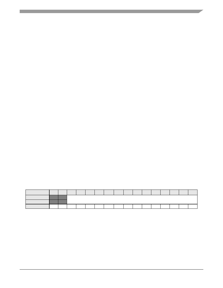
Register Descriptions
56F8013 Technical Data, Rev. 2
Freescale Semiconductor
55
Preliminary
5.6.5.3 Reload PWM Interrupt Priority Level (PWM_RL IPL)--
Bits 5≠4
This field is used to set the interrupt priority level for IRQs. This IRQ is limited to priorities 0 through 2.
They are disabled by default.
∑
00 = IRQ disabled (default)
∑
01 = IRQ is priority level 0
∑
10 = IRQ is priority level 1
∑
11 = IRQ is priority level 2
5.6.5.4 ADC Zero Crossing or Limit Error Interrupt Priority Level
(ADC_ZC_LE IPL)-- Bits 3≠2
This field is used to set the interrupt priority level for IRQs. This IRQ is limited to priorities 0 through 2.
They are disabled by default.
∑
00 = IRQ disabled (default)
∑
01 = IRQ is priority level 0
∑
10 = IRQ is priority level 1
∑
11 = IRQ is priority level 2
5.6.5.5 ADCB Conversion Complete Interrupt Priority Level
(ADCB_CC IPL)--Bits 1≠0
This field is used to set the interrupt priority level for IRQs. This IRQ is limited to priorities 0 through 2.
They are disabled by default.
∑
00 = IRQ disabled (default)
∑
01 = IRQ is priority level 0
∑
10 = IRQ is priority level 1
∑
11 = IRQ is priority level 2
5.6.6
Vector Base Address Register (VBA)
Figure 5-8 Vector Base Address Register (VBA)
5.6.6.1 Reserved--Bits 15≠14
This bit field is reserved or not implemented. It is read as 0 and cannot be modified by writing.
Base + $5
15
14
13
12
11
10
9
8
7
6
5
4
3
2
1
0
Read
0
0
VECTOR_BASE_ADDRESS
Write
RESET
0
0
0
0
0
0
0
0
0
0
0
0
0
0
0
0
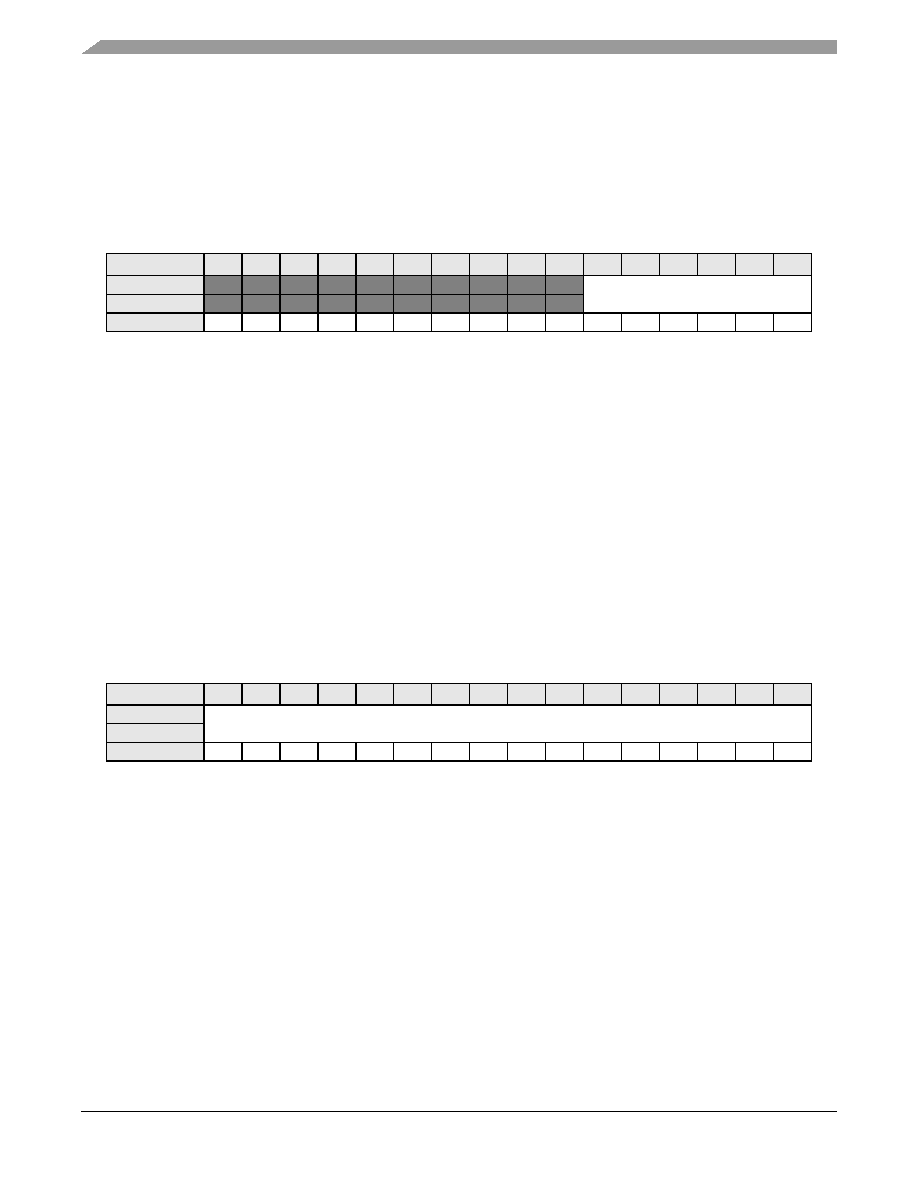
56F8013 Technical Data, Rev. 2
56
Freescale Semiconductor
Preliminary
5.6.6.2 Vector Address Bus (VAB) Bits 13--0
The value in this register is used as the upper 14 bits of the interrupt vector VAB[20:0]. The lower 7 bits
are determined based on the highest priority interrupt and are then appended onto VBA before presenting
the full VAB to the Core.
5.6.7
Fast Interrupt Match 0 Register (FIM0)
Figure 5-9 Fast Interrupt Match 0 Register (FIM0)
5.6.7.1 Reserved--Bits 15≠6
This bit field is reserved or not implemented. It is read as 0 and cannot be modified by writing.
5.6.7.2 Fast Interrupt 0 Vector Number (FAST INTERRUPT 0)--Bits 5≠0
These values determine which IRQ will be Fast Interrupt 0. Fast Interrupts vector directly to a service
routine based on values in the Fast Interrupt Vector Address registers without having to go to a jump table
first. IRQs used as Fast Interrupts must be set to priority level 2. Unexpected results will occur if a Fast
Interrupt vector is set to any other priority. A Fast Interrupt automatically becomes the highest-priority
level 2 interrupt regardless of its location in the interrupt table prior to being declared as Fast Interrupt.
Fast Interrupt 0 has priority over Fast Interrupt 1. To determine the vector number of each IRQ, refer to
the vector table.
5.6.8
Fast Interrupt 0 Vector Address Low Register (FIVAL0)
Figure 5-10 Fast Interrupt 0 Vector Address Low Register (FIVAL0)
5.6.8.1 Fast Interrupt 0 Vector Address Low (FIVAL0)--Bits 15--0
The lower 16 bits of the vector address used for Fast Interrupt 0. This register is combined with FIVAH0
to form the 21-bit vector address for Fast Interrupt 0 defined in the FIM0 register.
Base + $6
15
14
13
12
11
10
9
8
7
6
5
4
3
2
1
0
Read
0
0
0
0
0
0
0
0
0
0
FAST INTERRUPT 0
Write
RESET
0
0
0
0
0
0
0
0
0
0
0
0
0
0
0
0
Base + $7
15
14
13
12
11
10
9
8
7
6
5
4
3
2
1
0
Read
FAST INTERRUPT 0 VECTOR ADDRESS LOW
Write
RESET
0
0
0
0
0
0
0
0
0
0
0
0
0
0
0
0

Register Descriptions
56F8013 Technical Data, Rev. 2
Freescale Semiconductor
57
Preliminary
5.6.9
Fast Interrupt 0 Vector Address High Register (FIVAH0)
Figure 5-11 Fast Interrupt 0 Vector Address High Register (FIVAH0)
5.6.9.1 Reserved--Bits 15≠5
This bit field is reserved or not implemented. It is read as 0 and cannot be modified by writing.
5.6.9.2 Fast Interrupt 0 Vector Address High (FIVAH0)--Bits 4≠0
The upper five bits of the vector address used for Fast Interrupt 0. This register is combined with FIVAL0
to form the 21-bit vector address for Fast Interrupt 0 defined in the FIM0 register.
5.6.10 Fast Interrupt 1 Match Register (FIM1)
Figure 5-12 Fast Interrupt 1 Match Register (FIM1)
5.6.10.1 Reserved--Bits 15≠6
This bit field is reserved or not implemented. It is read as 0 and cannot be modified by writing.
5.6.10.2 Fast Interrupt 1 Vector Number (FAST INTERRUPT 1)--Bits 5≠0
These values determine which IRQ will be Fast Interrupt 1. Fast Interrupts vector directly to a service
routine based on values in the Fast Interrupt Vector Address registers without having to go to a jump table
first. IRQs used as Fast Interrupts must be set to priority level 2. Unexpected results will occur if a Fast
Interrupt vector is set to any other priority. A Fast Interrupt automatically becomes the highest priority
level 2 interrupt, regardless of its location in the interrupt table prior to being declared as Fast Interrupt.
Fast Interrupt 0 has priority over Fast Interrupt 1. To determine the vector number of each IRQ, refer to
the vector table.
Base + $8
15
14
13
12
11
10
9
8
7
6
5
4
3
2
1
0
Read
0
0
0
0
0
0
0
0
0
0
0
FAST INTERRUPT 0 VECTOR
ADDRESS HIGH
Write
RESET
0
0
0
0
0
0
0
0
0
0
0
0
0
0
0
0
Base + $9
15
14
13
12
11
10
9
8
7
6
5
4
3
2
1
0
Read
0
0
0
0
0
0
0
0
0
0
FAST INTERRUPT 1
Write
RESET
0
0
0
0
0
0
0
0
0
0
0
0
0
0
0
0
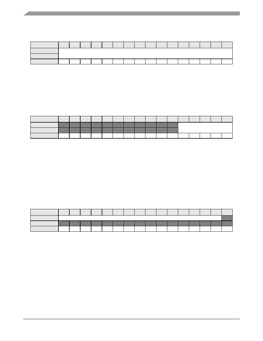
56F8013 Technical Data, Rev. 2
58
Freescale Semiconductor
Preliminary
5.6.11 Fast Interrupt 1 Vector Address Low Register (FIVAL1)
Figure 5-13 Fast Interrupt 1 Vector Address Low Register (FIVAL1)
5.6.11.1 Fast Interrupt 1 Vector Address Low (FIVAL1)--Bits 15≠0
The lower 16 bits of the vector address used for Fast Interrupt 1. This register is combined with FIVAH1
to form the 21-bit vector address for Fast Interrupt 1 defined in the FIM1 register.
5.6.12 Fast Interrupt 1 Vector Address High (FIVAH1)
Figure 5-14 Fast Interrupt 1 Vector Address High Register (FIVAH1)
5.6.12.1 Reserved--Bits 15≠5
This bit field is reserved or not implemented. It is read as 0 and cannot be modified by writing.
5.6.12.2 Fast Interrupt 1 Vector Address High (FIVAH1)--Bits 4≠0
The upper five bits of the vector address used for Fast Interrupt 1. This register is combined with FIVAL1
to form the 21-bit vector address for Fast Interrupt 1 defined in the FIM1 register.
5.6.13 IRQ Pending Register 0 (IRQP0)
Figure 5-15 IRQ Pending Register 0 (IRQP0)
5.6.13.1 IRQ Pending (PENDING)--Bits 15≠1
This register combines with IRQP1 and IRQP2 to represent the pending IRQs for interrupt vector numbers
2 through 45.
∑
0 = IRQ pending for this vector number
∑
1 = No IRQ pending for this vector number
5.6.13.2 Reserved--Bit 0
This bit is reserved or not implemented. It is read as 1 and cannot be modified by writing.
Base + $A
15
14
13
12
11
10
9
8
7
6
5
4
3
2
1
0
Read
FAST INTERRUPT 1 VECTOR ADDRESS LOW
Write
RESET
0
0
0
0
0
0
0
0
0
0
0
0
0
0
0
0
Base + $B
15
14
13
12
11
10
9
8
7
6
5
4
3
2
1
0
Read
0
0
0
0
0
0
0
0
0
0
0
FAST INTERRUPT 1 VECTOR
ADDRESS HIGH
Write
RESET
0
0
0
0
0
0
0
0
0
0
0
0
0
0
0
0
Base + $C
15
14
13
12
11
10
9
8
7
6
5
4
3
2
1
0
Read
PENDING[16:2]
1
Write
RESET
1
1
1
1
1
1
1
1
1
1
1
1
1
1
1
1

Register Descriptions
56F8013 Technical Data, Rev. 2
Freescale Semiconductor
59
Preliminary
5.6.14 IRQ Pending Register 1 (IRQP1)
Figure 5-16 IRQ Pending Register 1 (IRQP1)
5.6.14.1 IRQ Pending (PENDING)--Bits 32≠17
This register combines with IRQP0 and IRQP2 to represent the pending IRQs for interrupt vector numbers
2 through 45.
∑
0 = IRQ pending for this vector number
∑
1 = No IRQ pending for this vector number
5.6.15 IRQ Pending Register 2 (IRQP2)
Figure 5-17 IRQ Pending Register 2 (IRQP2)
5.6.15.1 IRQ Pending (PENDING)--Bits 45≠33
This register combines with IRQP0 and IRQP1 to represent the pending IRQs for interrupt vector numbers
2 through 45.
∑
0 = IRQ pending for this vector number
∑
1 = No IRQ pending for this vector number
5.6.16 Interrupt Control Register (ICTRL)
Figure 5-18 Interrupt Control Register (ICTRL)
5.6.16.1 Interrupt (INT)--Bit 15
This read-only bit reflects the state of the interrupt to the 56800E core.
∑
0 = No interrupt is being sent to the 56800E core
∑
1 = An interrupt is being sent to the 56800E core
Base + $D
15
14
13
12
11
10
9
8
7
6
5
4
3
2
1
0
Read
PENDING[32:17]
Write
RESET
1
1
1
1
1
1
1
1
1
1
1
1
1
1
1
1
Base + $E
15
14
13
12
11
10
9
8
7
6
5
4
3
2
1
0
Read
1
1
1
PENDING[45:33]
Write
RESET
1
1
1
1
1
1
1
1
1
1
1
1
1
1
1
1
$Base + $12
15
14
13
12
11
10
9
8
7
6
5
4
3
2
1
0
Read
INT
IPIC
VAB
INT_
DIS
1
1
1
0
0
Write
RESET
0
0
0
0
0
0
0
0
0
0
0
1
1
1
0
0

56F8013 Technical Data, Rev. 2
60
Freescale Semiconductor
Preliminary
5.6.16.2 Interrupt Priority Level (IPIC)--Bits 14≠13
These read-only bits reflect the state of the new interrupt priority level bits being presented to the 56800E
core. These bits indicate the priority level needed for a new IRQ to interrupt the current interrupt being
sent to the 56800E core. This field is only updated when the 56800E core jumps to a new interrupt service
routine.
Note:
Nested interrupts may cause this field to be updated before the original interrupt service routine can
read it.
∑
00 = Required nested exception priority levels are 0, 1, 2, or 3
∑
01 = Required nested exception priority levels are 1, 2, or 3
∑
10 = Required nested exception priority levels are 2 or 3
∑
11 = Required nested exception priority level is 3
5.6.16.3 Vector Number - Vector Address Bus (VAB)--Bits 12≠6
This read-only field shows the vector number (VAB[6:0]) used at the time the last IRQ was taken. In the
case of a Fast Interrupt, it shows the lower address bits of the jump address. This field is only updated when
the 56800E core jumps to a new interrupt service routine.
Note:
Nested interrupts may cause this field to be updated before the original interrupt service routine can
read it.
5.6.16.4 Interrupt Disable (INT_DIS)--Bit 5
This bit allows all interrupts to be disabled.
∑
0 = Normal operation (default)
∑
1 = All interrupts disabled
5.6.16.5 Reserved--Bits 4≠2
This bit field is reserved or not implemented. It is read as 1 and cannot be modified by writing.
5.6.16.6 Reserved--Bits 1≠0
This bit field is reserved or not implemented. It is read as 0 and cannot be modified by writing.
Table 5-3 Interrupt Priority Encoding
IPIC_VALUE[1:0]
Current Interrupt
Priority Level
Required Nested
Exception Priority
00
No interrupt or SWILP
Priorities 0, 1, 2, 3
01
Priority 0
Priorities 1, 2, 3
10
Priority 1
Priorities 2, 3
11
Priority 2 or 3
Priority 3

Resets
56F8013 Technical Data, Rev. 2
Freescale Semiconductor
61
Preliminary
5.7 Resets
5.7.1
General
5.7.2
Description of Reset Operation
5.7.2.1 Reset Handshake Timing
The ITCN provides the 56800E core with a reset vector address on the VAB pins whenever RESET is
asserted from the SIM. The reset vector will be presented until the second rising clock edge after RESET
is released. The general timing is shown in
Figure 5-19
.
Figure 5-19 Reset Interface
5.7.3
ITCN After Reset
After reset, all of the ITCN registers are in their default states. This means all interrupts are disabled,
except the core IRQs with fixed priorities:
∑
Illegal Instruction
∑
SW Interrupt 3
∑
HW Stack Overflow
∑
Misaligned Long Word Access
∑
SW Interrupt 2
∑
SW Interrupt 1
∑
SW Interrupt 0
∑
SW Interrupt LP
These interrupts are enabled at their fixed priority levels.
Table 5-4 Reset Summary
Reset
Priority
Source
Characteristics
Core Reset
RST
Core reset from the SIM
RES
CLK
VAB
PAB
RESET_VECTOR_ADR
READ_ADR

56F8013 Technical Data, Rev. 2
62
Freescale Semiconductor
Preliminary
Part 6 System Integration Module (SIM)
6.1 Introduction
The SIM module is a system catchall for the glue logic that ties together the system-on-chip. It controls
distribution of resets and clocks and provides a number of control features. The System Integration Module
is responsible for the following functions:
∑
Reset sequencing
∑
Clock control & distribution
∑
Stop/Wait control
∑
System status registers
∑
Registers for software access to the JTAG ID of the chip
∑
Test registers
∑
Power control
∑
I/O pad multiplexing
These are discussed in more detail in the sections that follow.
6.2 Features
The SIM has the following features:
∑
System bus clocks with pipeline hold-off support
∑
System clocks for non-pipelined interfaces
∑
Peripheral clocks for TMR and PWM with high-speed (3X) option
∑
Power-saving clock gating for peripherals
∑
ITCK clock to the
56800E
core TAP interface
∑
Three power modes (Run, Wait, Stop) to control power utilization
-- Stop mode shuts down the 56800E core, system clock, and peripheral clock
-- Wait mode shuts down the 56800E core and unnecessary system clock operation
-- Run mode supports full part operation
∑
Controls, with write protection, the enable/disable of 56800E core WAIT and STOP instructions
∑
Controls, with write protection, the enable/disable of Large Regulator Standby mode
∑
Controls to route functional signals to selected peripherals and I/O pads
∑
Controls deassertion sequence of internal resets
∑
Software-initiated reset
∑
Four 16-bit registers reset only by a Power-On Reset usable for general-purpose software control
∑
Timer channel Stop mode clocking controls
∑
SCI Stop mode clocking control to support LIN Sleep mode stop recovery
∑
Short addressing location control
∑
Registers for software access to the JTAG ID of the chip
∑
Controls output to CLKO pin
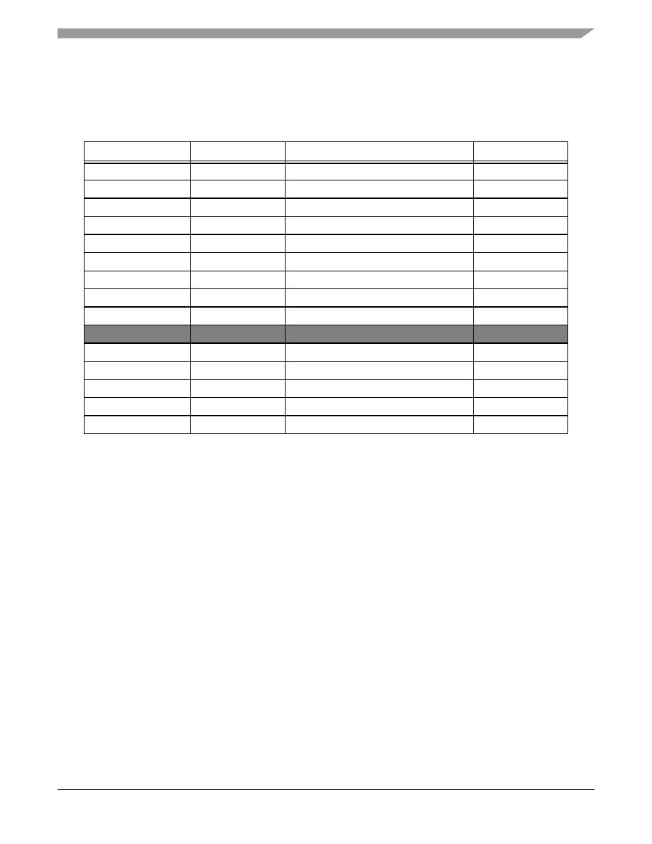
Register Descriptions
56F8013 Technical Data, Rev. 2
Freescale Semiconductor
63
Preliminary
6.3 Register Descriptions
Table 6-1 SIM Registers (SIM_BASE = $00 F140)
Address Offset
Address Acronym
Register Name
Section Location
Base + $0
SIM_CTRL
Control Register
6.3.1
Base + $1
SIM_RSTAT
Reset Status Register
6.3.2
Base + $2
SIM_SWC0
Software Control Register 0
6.3.3
Base + $3
SIM_SWC1
Software Control Register 1
6.3.3
Base + $4
SIM_SWC2
Software Control Register 2
6.3.3
Base + $5
SIM_SWC3
Software Control Register 3
6.3.3
Base + $6
SIM_MSHID
Most Significant Half of JTAG ID
6.3.4
Base + $7
SIM_LSHID
Least Significant Half of JTAG ID
6.3.5
Base + $8
SIM_PWR
Power Control Register
6.3.6
Reserved
Base + $A
SIM_CLKOUT
CLKO Select Register
6.3.7
Base + $B
SIM_GPS
GPIO Peripheral Select Register
6.3.8
Base + $C
SIM_PCE
Peripheral Clock Enable Register
6.3.9
Base + $D
SIM_IOSAHI
I/O Short Address Location High Register
6.3.10
Base + $E
SIM_IOSALO
I/O Short Address Location Low Register
6.3.10
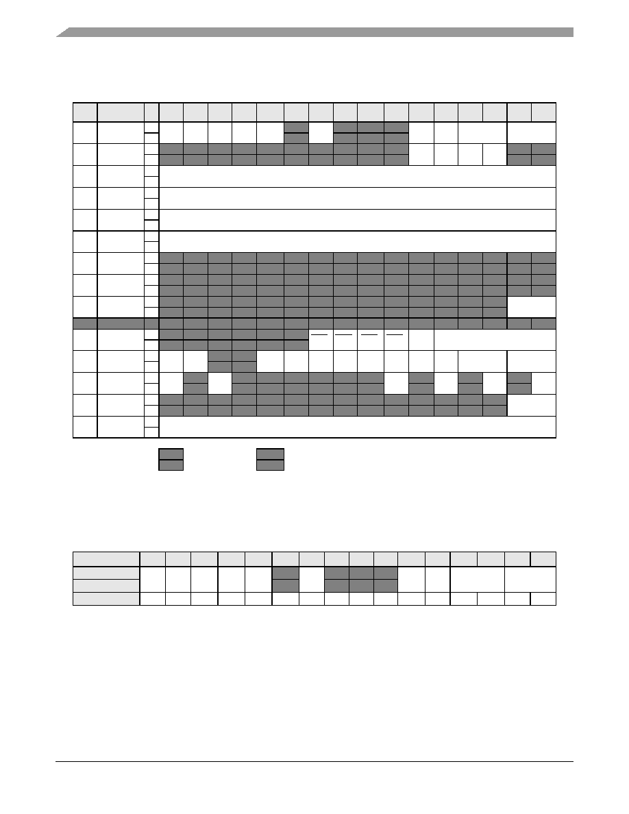
56F8013 Technical Data, Rev. 2
64
Freescale Semiconductor
Preliminary
Figure 6-1 SIM Register Map Summary
6.3.1
SIM Control Register (SIM_CTRL)
Figure 6-2 SIM Control Register (SIM_CTRL)
Add.
Offset
Address
Acronym
15
14
13
12
11
10
9
8
7
6
5
4
3
2
1
0
$0
SIM_
CTRL
R
TC3_
SD
TC2_
SD
TC1_
SD
TC0_
SD
SCI_
SD
0
TC3_
INP
0
0
0
ONCE
EBL
0
SW
RST
STOP_
DISABLE
WAIT_
DISABLE
W
$1
SIM_
RSTAT
R
0
0
0
0
0
0
0
0
0
0
SWR COPR EXTR
POR
0
0
W
$2
SIM_SWC0
R
Software Control Data 0
W
$3
SIM_SWC1
R
Software Control Data 1
W
$4
SIM_SWC2
R
Software Control Data 2
W
$5
SIM_SWC3
R
Software Control Data 3
W
$6
SIM_MSHID
R
0
0
0
0
0
0
0
1
1
1
1
1
0
0
1
0
W
$7
SIM_LSHID
R
0
1
0
0
0
0
0
0
0
0
0
1
1
1
0
1
W
$8
SIM_PWR
R
0
0
0
0
0
0
0
0
0
0
0
0
0
0
LRSTDBY
W
Reserved
$A
SIM_
CLKOUT
R
0
0
0
0
0
0
PWM3 PWM2 PWM1 PWM0
CLK
DIS
CLKOSEL
W
$B
SIM_GPS
R
TCR
PCR
0
0
CFG_
B7
CFG_
B6
CFG_
B5
CFG_
B4
CFG_
B3
CFG_
B2
CFG_
B1
CFG_
B0
CFG_A5
CFG_A4
W
$C
SIM_PCE
R
I2C
0
ADC
0
0
0
0
0
0
TMR
0
SCI
0
SPI
0
PWM
W
$D
SIM_IOSAHI
R
0
0
0
0
0
0
0
0
0
0
0
0
0
0
ISAL[23:22]
W
$E
SIM_IOSALO
R
ISAL[21:6]
W
0
= Read as 0
1
=
Read as 1
= Reserved
= Reserved
Base + $0
15
14
13
12
11
10
9
8
7
6
5
4
3
2
1
0
Read
TC3_
SD
TC2_
SD
TC1_
SD
TC0_
SD
SCI_
SD
0
TC3_
INP
0
0
0
ONCE
EBL
SW
RST
STOP_
DISABLE
WAIT_
DISABLE
Write
RESET
0
0
0
0
0
0
0
0
0
0
0
0
0
0
0
0

Register Descriptions
56F8013 Technical Data, Rev. 2
Freescale Semiconductor
65
Preliminary
6.3.1.1 Timer Channel 3 Stop Disable (TC3_SD)--Bit 15
This bit enables the operation of the Timer Channel 3 peripheral clock in Stop mode.
∑
0 = Timer Channel 3 disabled in Stop mode
∑
1 = Timer Channel 3 enabled in Stop mode
6.3.1.2 Timer Channel 2 Stop Disable (TC2_SD)--Bit 14
This bit enables the operation of the Timer Channel 2 peripheral clock in Stop mode.
∑
0 = Timer Channel 2 disabled in Stop mode
∑
1 = Timer Channel 2 enabled in Stop mode
6.3.1.3 Timer Channel 1 Stop Disable (TC1_SD)--Bit 13
This bit enables the operation of the Timer Channel 1 peripheral clock in Stop mode.
∑
0 = Timer Channel 1 disabled in Stop mode
∑
1 = Timer Channel 1 enabled in Stop mode
6.3.1.4 Timer Channel 0 Stop Disable (TC0_SD)--Bit 12
This bit enables the operation of the Timer Channel 0 peripheral clock in Stop mode.
∑
0 = Timer Channel 0 disabled in Stop mode
∑
1 = Timer Channel 0 enabled in Stop mode
6.3.1.5 SCI Stop Disable (SCI_SD)--Bit 11
This bit enables the operation of the SCI peripheral clock in Stop mode. This is recommended for use in
LIN mode so that the SCI can generate interrupts and recover from Stop mode while the LIN interface is
in Sleep mode and using Stop mode to reduce power consumption.
∑
0 = SCI disabled in Stop mode
∑
1 = SCI enabled in Stop mode
6.3.1.6 Reserved--Bit 10
This bit field is reserved or not implemented. It is read as 0 and cannot be modified by writing.
6.3.1.7 Timer Channel 3 Input (TC3_INP)--Bit 9
This bit selects the input of Timer Channel 3 to be from the PWM or GPIO.
∑
0 = Timer Channel 3 Input from PWM reload_sync signal
∑
1 = Timer Channel 3 Input controlled by SIM_GPS register CFG_B3 and CFG_A5 fields

56F8013 Technical Data, Rev. 2
66
Freescale Semiconductor
Preliminary
6.3.1.8 Reserved--Bits 8≠6
This bit field is reserved or not implemented. It is read as 0 and cannot be modified by writing.
6.3.1.9 OnCE Enable (ONCEEBL)--Bit 5
∑
0 = OnCE clock to 56800E core enabled when core TAP is enabled
∑
1 = OnCE clock to 56800E core is always enabled
6.3.1.10 Software Reset (SWRST)--Bit 4
Writing 1 to this field will cause the part to reset.
6.3.1.11 Stop Disable (STOP_DISABLE[1:0])--Bits 3≠2
∑
00 = Stop mode will be entered when the 56800E core executes a STOP instruction
∑
01 = The 56800E STOP instruction will not cause entry into Stop mode
∑
10 = Stop mode will be entered when the 56800E core executes a STOP instruction and the
STOP_DISABLE field is write-protected until the next reset
∑
11 = The 56800E STOP instruction will not cause entry into Stop mode and the STOP_DISABLE field is
write-protected until the next reset
6.3.1.12 Wait Disable (WAIT_DISABLE[1:0])--Bits 1≠0
∑
00 = Wait mode will be entered when the 56800E core executes a WAIT instruction
∑
01 = The 56800E WAIT instruction will not cause entry into Wait mode
∑
10 = Wait mode will be entered when the 56800E core executes a WAIT instruction and the
WAIT_DISABLE field is write-protected until the next reset
∑
11 = The 56800E WAIT instruction will not cause entry into Wait mode and the WAIT_DISABLE field is
write-protected until the next reset
6.3.2
SIM Reset Status Register (SIM_RSTAT)
This register is updated upon any system reset and indicates the cause of the most recent reset. It also
controls whether the COP reset vector or regular reset vector in the vector table is used. This register is
asynchronously reset during Power-On Reset (see power supervisor module) and subsequently is
synchronously updated based on the level of the external reset, software reset, or cop reset inputs. Only
one source will ever be indicated. In the event that multiple reset sources assert simultaneously, the
highest-precedence source will be indicated. The precedence from highest to lowest is POR, EXTR,
COPR, and SWR. While POR is always set during a Power-On Reset, EXTR will become set if the
external reset pin is asserted or remains asserted after the Power-On Reset (POR) has deasserted.
Figure 6-3 SIM Reset Status Register (SIM_RSTAT)
Base + $1
15
14
13
12
11
10
9
8
7
6
5
4
3
2
1
0
Read
0
0
0
0
0
0
0
0
0
0
SWR
COPR
EXTR
POR
0
0
Write
RESET
0
0
0
0
0
0
0
0
0
0
0
0
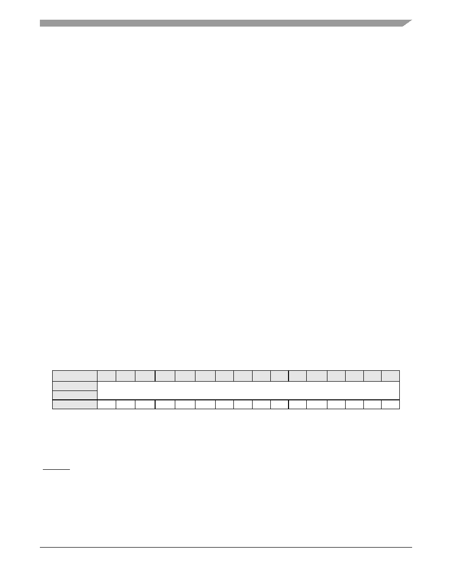
Register Descriptions
56F8013 Technical Data, Rev. 2
Freescale Semiconductor
67
Preliminary
6.3.2.1 Reserved--Bits 15≠6
This bit field is reserved or not implemented. It is read as zero and cannot be modified by writing.
6.3.2.2 Software Reset (SWR)--Bit 5
When set, this bit indicates that the previous system reset occurred as a result of a software reset (written
1 to SWRST bit in the SIM_CTRL register). It will not be set if a COP, external, or POR reset also
occurred.
6.3.2.3 COP Reset (COPR)--Bit 4
When set, this bit indicates that the previous system reset was caused by the Computer Operating Properly
(COP) timer. It will not be set if an external or POR reset also occurred. If COPR is set as code starts
executing, the COP reset vector in the vector table will be used. Otherwise, the normal reset vector is used.
6.3.2.4 External Reset (EXTR)--Bit 3
When set, this bit indicates that the previous system reset was caused by an external reset. It will only be
set if the external reset pin was asserted or remained asserted after the Power-On Reset deasserted.
6.3.2.5 Power-On Reset (POR)--Bit 2
This bit is set during a Power-On Reset.
6.3.2.6 Reserved--Bits 1≠0
This bit field is reserved or not implemented. It is read as 0 and cannot be modified by writing.
6.3.3
SIM Software Control Registers (SIM_SWC0, SIM_SWC1,
SIM_SWC2, and SIM_SWC3)
Only SIM_SWC0 is shown in this section. SIM_SWC1, SIM_SWC2, and SIM_SWC3 are identical in
functionality.
Figure 6-4 SIM Software Control Register 0 (SIM_SWC0)
6.3.3.1 Software Control Data 0 (FIELD)--Bits 15≠0
This register is reset only by the Power-On Reset (POR). It has no part-specific functionality and is
intended for use by a software developer to contain data that will be unaffected by the other reset sources
(RESET pin, software reset, and COP reset).
Base + $2
15
14
13
12
11
10
9
8
7
6
5
4
3
2
1
0
Read
Software Control Data 0
Write
RESET
0
0
0
0
0
0
0
0
0
0
0
0
0
0
0
0

56F8013 Technical Data, Rev. 2
68
Freescale Semiconductor
Preliminary
6.3.4
Most Significant Half of JTAG ID (SIM_MSHID)
This read-only register displays the most significant half of the JTAG ID for the chip. This register reads
$01F2.
Figure 6-5 Most Significant Half of JTAG ID (SIM_MSHID)
6.3.5
Least Significant Half of JTAG ID (SIM_LSHID)
This read-only register displays the least significant half of the JTAG ID for the chip. This register reads
$401D.
Figure 6-6 Least Significant Half of JTAG ID (SIM_LSHID)
6.3.6
SIM Power Control Register (SIM_PWR)
This register controls the Standby mode of the large regulator. The large regulator derives the core digital
logic power supply from the IO power supply. In some circumstances, the large regulator may be put in a
reduced-power Standby mode without interfering with part operation. Refer to the overview of
power-down modes and the overview of clock generation for more information on the use of large
regulator standby.
Figure 6-7 SIM Power Control Register (SIM_PWR)
6.3.6.1 Reserved--Bits 15≠2
This bit field is reserved or not implemented. It is read as 0 and cannot be modified by writing.
Base + $6
15
14
13
12
11
10
9
8
7
6
5
4
3
2
1
0
Read
0
0
0
0
0
0
0
1
1
1
1
1
0
0
1
0
Write
RESET
0
0
0
0
0
0
0
1
1
1
1
1
0
0
1
0
Base + $7
15
14
13
12
11
10
9
8
7
6
5
4
3
2
1
0
Read
0
1
0
0
0
0
0
0
0
0
0
1
1
1
0
1
Write
RESET
0
1
0
0
0
0
0
0
0
0
0
1
1
1
0
1
Base + $8
15
14
13
12
11
10
9
8
7
6
5
4
3
2
1
0
Read
0
0
0
0
0
0
0
0
0
0
0
0
0
0
LRSTDBY
Write
RESET
0
0
0
0
0
0
0
0
0
0
0
0
0
0
0
0

Register Descriptions
56F8013 Technical Data, Rev. 2
Freescale Semiconductor
69
Preliminary
6.3.6.2 Large Regulator Standby Mode[1:0] (LRSTDBY)--Bits 1≠0
This bit controls the pull-up resistors on the IRQA pin.
∑
00 = Large regulator is in Normal mode
∑
01 = Large regulator is in Standby (reduced-power) mode
∑
10 = Large regulator is in Normal mode and the LRSTDBY field is write-protected until the next reset
∑
11 = Large regulator is in Standby mode and the LRSTDBY field is write-protected until the next reset
6.3.7
CLKO Select Register (SIM_CLKOUT)
The CLKO select register can be used to multiplex out selected clocks generated inside the clock
generation and SIM modules. All functionality is for test purposes only and is subject to
unspecified latencies. Glitches may be produced when the clock is enabled or switched.
The lower four bits of the GPIO A register can function as GPIO, PWM, or as additional clock output
signals. GPIO has priority and is enabled/disabled via the GPIOA_PEREN. If GPIOA[3:0] are
programmed to operate as peripheral outputs, then the choice between PWM and additional clock outputs
is done here in the CLKOUT. The default state is for the peripheral function of GPIOA[3:0] to be
programmed as PWM. This can be changed by altering PWM3 through PWM0.
Figure 6-8 CLKO Select Register (SIM_CLKOUT)
6.3.7.1 Reserved--Bits 15≠10
This bit field is reserved or not implemented. It is read as 0 and cannot be modified by writing.
6.3.7.2 PWM3--Bit 9
∑
0 = Peripheral output function of GPIOA[3] is defined to be PWM3
∑
1 = Peripheral output function of GPIOA[3] is defined to be the Relaxation Oscillator Clock
6.3.7.3 PWM2--Bit 8
∑
0 = Peripheral output function of GPIOA[2] is defined to be PWM2
∑
1 = Peripheral output function of GPIOA[2] is defined to be the system clock
6.3.7.4 PWM1--Bit 7
∑
0 = Peripheral output function of GPIOA[1] is defined to be PWM1
∑
1 = Peripheral output function of GPIOA[1] is defined to be two times the rate of the system clock
Base + $A
15
14
13
12
11
10
9
8
7
6
5
4
3
2
1
0
Read
0
0
0
0
0
0
PWM3
PWM2 PWM1 PWM0
CLK
DIS
CLKOSEL
Write
RESET
0
0
0
0
0
0
0
0
0
0
1
0
0
0
0
0

56F8013 Technical Data, Rev. 2
70
Freescale Semiconductor
Preliminary
6.3.7.5 PWM0--Bit 6
∑
0 = Peripheral output function of GPIOA[0] is defined to be PWM0
∑
1 = Peripheral output function of GPIOA[0] is defined to be three times the rate of the system clock
6.3.7.6 Clockout Disable (CLKDIS)--Bit 5
∑
0 = CLKOUT output is enabled and will output the signal indicated by CLKOSEL
∑
1 = CLKOUT is 0
6.3.7.7 Clockout Select (CLKOSEL)--Bits 4≠0
Selects clock to be muxed out on the CLKO pin.
∑
00000 = Reserved for factory test--Continuous system clock
∑
01001 = Reserved for factory test--OCCS MSTR OSC clock
∑
01011 = Reserved for factory test--ADC clock
∑
01100 = Reserved for factory test--JTAG TCLK
∑
01101 = Reserved for factory test--Continuous peripheral clock
∑
01110 = Reserved for factory test--Continuous inverted peripheral clock
∑
01111 = Reserved for factory test--Continuous high-speed peripheral clock
6.3.8
SIM GPIO Peripheral Select Register (SIM_GPS)
All of the peripheral pins on the 56F8013 share their Input/Output (I/O) with GPIO ports. In order to select
peripheral or GPIO control, program the GPIOx_PEREN register. In some cases, there are two possible
peripherals as well as the GPIO functionality available for control of the I/O. In these cases, the SIM_GPS
register is used to determine which peripheral has control.
As shown in
Figure 6-9
, the GPIO Peripheral Enable Register (PEREN) has the final control over which
pin controls the I/O. SIM_GPS simply decides which peripheral will be routed to the I/O when
PEREN = 1.
Figure 6-9 Overall Control of Pads Using SIM_GPS Control
GPIOB_PEREN Register
GPIO Controlled
I/O
Pad Control
SIM_GPS Register
Quad Timer Controlled
SCI Controlled
0
1
0
1

Register Descriptions
56F8013 Technical Data, Rev. 2
Freescale Semiconductor
71
Preliminary
Figure 6-10 GPIO Peripheral Select Register (SIM_GPS)
6.3.8.1 TMR Clock Rate (TCR)--Bit 15
This bit selects the clock speed for the TMR module.
∑
0 = TMR module clock rate equals core clock rate, typically 32MHz (default)
∑
1 = TMR module clock rate equals three times core clock rate
Note: This bit should only be changed while the TMR module's clock is disabled. See
Section 6.3.9
.
Note: High-speed clocking is only available when the PLL is being used.
Note: If the PWM reload pulse is used as input to Timer 3 (See SIM_CTRL: TC3_INP,
Section 6.3.1.7
),
then the clocks of the Quad Timer and PWM must be related, as shown in
Table 6-2
.
6.3.8.2 PWM Clock Rate (PCR)--Bit 14
This bit selects the clock speed for the PWM module.
∑
0 = PWM module clock rate equals core clock rate, typically 32MHz (default)
∑
1 = PWM module clock rate equals three times core clock rate
Note: This bit should only be changed while the
PWM
module's clock is disabled. See
Section 6.3.9
.
Note: High-speed clocking is only available when the PLL is being used.
Note: If the PWM reload pulse is used as input to Timer 3 (See SIM_CTRL: TC3_INP,
Section 6.3.1.7
),
then the clocks of the Quad Timer and PWM must be related, as shown in
Table 6-2
.
Base + $B
15
14
13
12
11
10
9
8
7
6
5
4
3
2
1
0
Read
TCR
PCR
0
0
CFG_
B7
CFG_
B6
CFG_
B5
CFG_
B4
CFG_
B3
CFG_
B2
CFG_
B1
CFG_
B0
CFG_A5
CFG_A4
Write
RESET
0
0
0
0
0
0
0
0
0
0
0
0
0
0
0
0
Table 6-2 Allowable Quad Timer and PWM Clock Rates
when Using PWM Reload Pulse
Quad Timer
Clock Speed
1X
3X
PWM
1X
OK
OK
3X
NO
OK

56F8013 Technical Data, Rev. 2
72
Freescale Semiconductor
Preliminary
6.3.8.3 Reserved--Bits 13≠12
This bit field is reserved or not implemented. It is read as 0 and cannot be modified by writing.
Note: Take care when programming the following CFG_* signals so as not to connect two
different I/O pads to the same peripheral input. For example, do not set CFG_B7 to select
SCL and also set CFG_B0 to select SCL. If this occurs for an output signal, then the signal
will be routed to two I/O pads. For input signals, the values on the two I/O pads will be
ORed together before reaching the peripheral.
6.3.8.4 Configure GPIOB7 (CFG_B7)--Bit 11
This bit selects the alternate function for GPIOB7.
∑
0 = TXD (default)
∑
1 = SCL
6.3.8.5 Configure GPIOB6 (CFG_B6)--Bit 10
This bit selects the alternate function for GPIOB6.
∑
0 = RXD (default)
∑
1 = SDA
Note: The CLKMODE bit in the OCCS Oscillator Control register can enable this pin as the
source clock to the chip. In this mode, make sure that no on-chip peripheral (including the
GPIO) is driving this pin.
6.3.8.6 Configure GPIOB5 (CFG_B5)--Bit 9
This bit selects the alternate function for GPIOB5.
∑
0 = T1 (default)
∑
1 = FAULT3
6.3.8.7 Configure GPIOB4 (CFG_B4)--Bit 8
This bit selects the alternate function for GPIOB4.
∑
0 = T0 (default)
∑
1 = CLKO
6.3.8.8 Configure GPIOB3 (CFG_B3)--Bit 7
This bit selects the alternate function for GPIOB3.
∑
0 = MOSI (default)
∑
1 = T3

Register Descriptions
56F8013 Technical Data, Rev. 2
Freescale Semiconductor
73
Preliminary
6.3.8.9 Configure GPIOB2 (CFG_B2)--Bit 6
This bit selects the alternate function for GPIOB2.
∑
0 = MISO (default)
∑
1 = T2
6.3.8.10 Configure GPIOB1 (CFG_B1)--Bit 5
This bit selects the alternate function for GPIOB1.
∑
0 = SS (default)
∑
1 = SDA
6.3.8.11 Configure GPIOB0 (CFG_B0)--Bit 4
This bit selects the alternate function for GPIOB0.
∑
0 = SCLK (default)
∑
1 = SCL
6.3.8.12 Configure GPIOA5[1:0] (CFG_A5)--Bits 3≠2
These bits select the alternate function for GPIOA5.
∑
00 = Select PWM5 when peripheral mode is enabled in GPIOA5 (default)
∑
01 = Select PWM5 when peripheral mode is enabled in GPIOA5
∑
10 = Select FAULT2 when peripheral mode is enabled in GPIOA5
∑
11 = Select T3 when peripheral mode is enabled in GPIOA5
6.3.8.13 Configure GPIOA4[1:0] (CFG_A4)--Bits 1≠0
These bits select the alternate function for GPIOA4.
∑
00 = Select PWM4 when peripheral mode is enabled in GPIOA4 (default)
∑
01 = Select PWM4 when peripheral mode is enabled in GPIOA4
∑
10 = Select FAULT1 when peripheral mode is enabled in GPIOA4
∑
11 = Select T2 when peripheral mode is enabled in GPIOA4
6.3.9
Peripheral Clock Enable Register (SIM_PCE)
The Peripheral Clock Enable register is used to enable or disable clocks to the peripherals as a power
savings feature. The clocks can be individually controlled for each peripheral on the chip. The
corresponding peripheral should itself be disabled while its clock is shut off. IPBus writes cannot be made
to a module that has its clock disabled.
Figure 6-11 Peripheral Clock Enable Register (SIM_PCE)
Base + $C
15
14
13
12
11
10
9
8
7
6
5
4
3
2
1
0
Read
I2C
0
ADC
0
0
0
0
0
0
TMR
0
SCI
0
SPI
0
PWM
Write
RESET
0
0
0
0
0
0
0
0
0
0
0
0
0
0
0
0

56F8013 Technical Data, Rev. 2
74
Freescale Semiconductor
Preliminary
6.3.9.1 I
2
C IPBus Clock Enable (I2C)--Bit 15
Each bit controls clocks to the indicated peripheral.
∑
0 = The clock is not provided to the peripheral (the peripheral is disabled)
∑
1 = Clocks are enabled
6.3.9.2 Reserved--Bit 14
This bit field is reserved or not implemented. It is read as 0 and cannot be modified by writing.
6.3.9.3 Analog-to-Digital Converter IPBus Clock Enable (ADC)--Bit 13
Each bit controls clocks to the indicated peripheral.
∑
0 = The clock is not provided to the peripheral (the peripheral is disabled)
∑
1 = Clocks are enabled
6.3.9.4 Reserved--Bits 12≠7
This bit field is reserved or not implemented. It is read as 0 and cannot be modified by writing.
6.3.9.5 Timer IPBus Clock Enable (TMR)--Bit 6
Each bit controls clocks to the indicated peripheral.
∑
0 = The clock is not provided to the peripheral (the peripheral is disabled)
∑
1 = Clocks are enabled
6.3.9.6 Reserved--Bit 5
This bit field is reserved or not implemented. It is read as 0 and cannot be modified by writing.
6.3.9.7 SCI IPBus Clock Enable (SCI)--Bit 4
Each bit controls clocks to the indicated peripheral.
∑
0 = The clock is not provided to the peripheral (the peripheral is disabled)
∑
1 = Clocks are enabled
6.3.9.8 Reserved--Bit 3
This bit field is reserved or not implemented. It is read as 0 and cannot be modified by writing.
6.3.9.9 SPI IPBus Clock Enable (SPI)--Bit 2
Each bit controls clocks to the indicated peripheral.
∑
0 = The clock is not provided to the peripheral (the peripheral is disabled)
∑
1 = Clocks are enabled
6.3.9.10 Reserved--Bit 1
This bit field is reserved or not implemented. It is read as 0 and cannot be modified by writing.
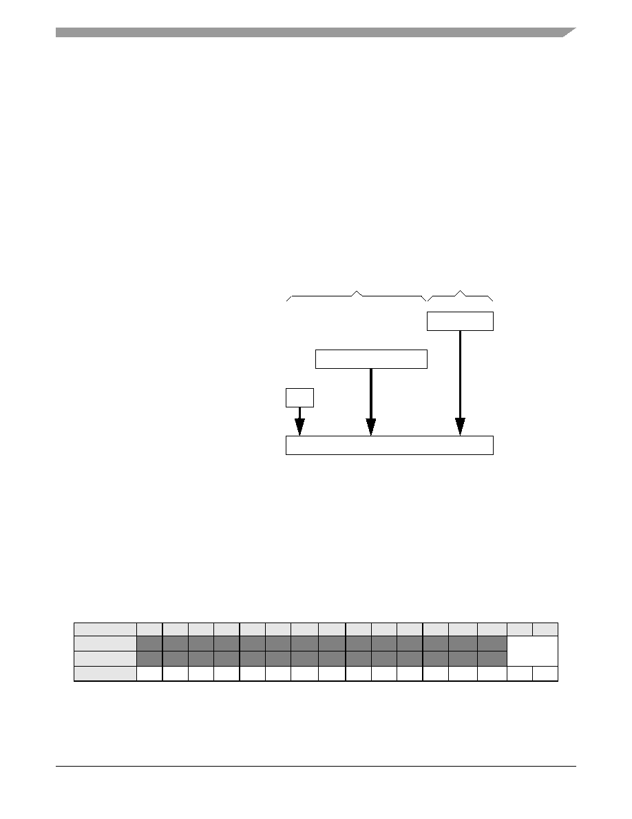
Register Descriptions
56F8013 Technical Data, Rev. 2
Freescale Semiconductor
75
Preliminary
6.3.9.11 PWM IPBus Clock Enable (PWM)--Bit 0
Each bit controls clocks to the indicated peripheral.
∑
0 = The clock is not provided to the peripheral (the peripheral is disabled)
∑
1 = Clocks are enabled
6.3.10 I/O Short Address Location Register (SIM_IOSAHI and
SIM_IOSALO)
The I/O Short Address Location registers are used to specify the memory referenced via the I/O short
address mode. The I/O short address mode allows the instruction to specify the lower six bits of address;
the upper address bits are not directly controllable. This register set allows limited control of the full
address, as shown in
Figure 6-12
.
Figure 6-12 I/O Short Address Determination
With this register set, an interrupt driver can set the SIM_IOSALO register pair to point to its peripheral
registers and then use the I/O Short addressing mode to reference them. The ISR should restore this register
to its previous contents prior to returning from interrupt.
Note:
The default value of this register set points to the EOnCE registers.
Note:
The pipeline delay between setting this register set and using short I/O addressing with the new value
is five instruction cycles.
Figure 6-13 I/O Short Address Location High Register (SIM_IOSAHI)
Base + $D
15
14
13
12
11
10
9
8
7
6
5
4
3
2
1
0
Read
0
0
0
0
0
0
0
0
0
0
0
0
0
0
ISAL[23:22]
Write
RESET
0
0
0
0
0
0
0
0
0
0
0
0
0
0
1
1
Instruction Portion
"
Hard Coded" Address Portion
6 Bits from I/O Short Address Mode Instruction
16 Bits from SIM_IOSALO Register
2 bits from SIM_IOSAHI Register
Full 24-Bit for Short I/O Address
56F8013 Technical Data, Rev. 2
76
Freescale Semiconductor
Preliminary
6.3.10.1 Reserved--Bits 15--2
This bit field is reserved or not implemented. It is read as 0 and cannot be modified by writing.
6.3.10.2 Input/Output Short Address Location (ISAL[23:22])--Bits 1≠0
This field represents the upper two address bits of the "hard coded" I/O short address.
Figure 6-14 I/O Short Address Location Low Register (SIM_IOSALO)
6.3.10.3 Input/Output Short Address Location (ISAL[21:6])--Bits 15≠0
This field represents the lower 16 address bits of the "hard coded" I/O short address.
6.4 Clock Generation Overview
The SIM uses master clocks from the OCCS module to produce the peripheral and system (core and
memory) clocks. The HS_PERF clock input from OCCS operates at three times the system and peripheral
bus rate, or a maximum of 96MHz. The SYS_CLK_x2 clock input from OCCS operates at two times the
system and peripheral bus rate, or a maximum of 64MHz. Peripheral and system clocks are generated at a
maximum of 32MHz by dividing the SYS_CLK_x2 clock by two and gating it with appropriate power
mode and clock gating controls. The PWM and TIMER peripheral clocks can optionally be generated at
three times the normal rate at a maximum of 96MHz. These clocks are generated by gating the HS_PERF
clock with appropriate power mode and clock gating controls.
The OCCS configuration controls the operating frequency of the SIM's master clocks. In the OCCS, either
an external clock or the relaxation oscillator can be selected as the master clock source (MSTR_OSC).
When selected, the relaxation oscillator can be operated at full speed (8MHz), standby speed (400kHz
using ROSB), or powered down (using ROPD). An 8MHz MSTR_OSC can be multiplied to 196MHz
using the PLL and postscaled to provide a variety of high speed clock rates. Either the postscaled PLL
output or MSTR_OSC signal can be selected to produce the master clocks to the SIM. When the PLL is
not selected, the HS_PERF clock is disabled and the SYS_CLK_x2 clock is MSTR_OSC.
In combination with the OCCS module, the SIM provides power modes (see
Section 6.5
), clock enables
(SIM_PCE register, CLK_DIS, ONCE_EBL), and clock rate controls (TCR, PCR) to
provide flexible
control of clocking and power utilization. The SIM's clock enable controls can be used to disable
individual clocks when not needed. The clock rate controls enable the high speed clocking option for the
Timer channels and PWM but require the PLL to be on and selected. Refer to the 56F8300 Peripheral
User Manual for further details.
Base + $E
15
14
13
12
11
10
9
8
7
6
5
4
3
2
1
0
Read
ISAL[21:6]
Write
RESET
1
1
1
1
1
1
1
1
1
1
1
1
1
1
1
1

Power-Down Modes
56F8013 Technical Data, Rev. 2
Freescale Semiconductor
77
Preliminary
6.5 Power-Down Modes
The 56F8013 operates in one of five Power-Down modes, as shown in
Table 6-3
.
The power modes provide additional means to disable clock domains, configure the voltage regulator, and
configure clock generation to manage power utilization, as shown in
Table 6-3
. Run, Wait, and Stop
modes provide means of enabling/disabling the peripheral and/or core clocking as a group. Stop disable
controls are provided for selected peripherals in the control register (SCI and TMR channels) so that these
Table 6-3 Clock Operation in Power-Down Modes
Mode
Core Clocks
Peripheral Clocks
Description
Run
Core and memory
clocks disabled
Peripheral clocks
enabled
Device is fully functional
Wait
Core and memory
clocks disabled
Peripheral clocks
enabled
Core executes WAIT instruction to enter this
mode.
Typically used for power-conscious applications.
Possible recoveries from Wait mode to Run
mode are:
1. Any interrupt
2. Executing a Debug mode entry command
during the 56800E core JTAG interface
2. Any reset (POR, external, software, COP)
Stop
Master clock generation in the OCCS
remains operational, but the SIM disables
the generation of system and peripheral
clocks.
Core executes STOP instruction to enter this
mode. Possible recoveries from Stop mode to
Run mode are:
1. Interrupt from TMR channels that have been
configured to operate in Stop mode (TCx_SD)
2. Interrupt for SCI configured to operate in Stop
mode (SCI_SD)
3. Low-voltage interrupt
4. Executing a Debug mode entry command
using the 56800E core JTAG interface
5. Any reset (POR, external, software, COP)
Standby
The OCCS generates the SYS_CLK_x2
clock at a reduced frequency (400kHz). The
PLL and HS_PERF clocks are disabled and
the high-speed peripheral option is not
available. System and peripheral clocks
operate at 200kHz.
The user configures the OCCS and SIM to select
the relaxation oscillator clock source (PRECS),
shut down the PLL (PLLPD), put the relaxation
oscillator in Standby mode (ROSB), and put the
large regulator in Standby (LRSTDBY). The part
is fully operational, but operating at a minimum
frequency and power configuration. Recovery
requires reversing the sequence used to enter
this mode (allowing for PLL lock time).
Power-Down
Master clock generation in the OCCS is
completely shut down. All system and
peripheral clocks are disabled.
The user configures the OCCS and SIM to enter
Standby mode as shown in the previous
description, followed by powering down the
oscillator (ROPD). The only possible recoveries
from this mode are:
1. External Reset
2. Power-On Reset

56F8013 Technical Data, Rev. 2
78
Freescale Semiconductor
Preliminary
peripheral clocks can optionally continue to operate in Stop mode and generate interrupts which will return
the part from Stop to Run mode. Standby mode provides normal operation but at very low speed and power
utilization. It is possible to invoke Stop or Wait mode while in Standby mode for even greater levels of
power reduction. A 400kHz clock external clock can optionally be used in Standby mode to produce the
required Standby 200kHz system bus rate. Power-down mode, which selects the ROSC clock source but
shuts it off, fully disables the part and minimizes its power utilization but is only recoverable via reset.
When the PLL is not selected and the system bus is operating at 200kHz or less, the large regulator can be
put into its Standby mode (LRSTDBY) to reduce the power utilization of that regulator.
All peripherals, except the COP/watchdog timer, run at the IPBus clock (peripheral bus) frequency
1
, which
is the same as the main processor frequency in this architecture. The COP timer runs at
MSTR_OSC / 1024. The maximum frequency of operation is SYS_CLK = 32MHz. The only exception is
the TMR and PWM, which can be configured to operate at three times the system bus rate using TCR and
PCR controls, provided the PLL is active and selected.
6.6 Resets
The SIM supports four sources of reset, as shown in
Figure 6-15
. The two asynchronous sources are the
external reset pin and the Power-On Reset (POR). The two synchronous sources are the software reset,
which is generated within the SIM itself by writing the SIM_CTRL register in
Section 6.3.1
, and the COP
reset. The SIM uses these to generate resets for the internal logic. These are outlined in
Table 6-4
. The
first column lists the four primary resets which are calculated. The JTAG circuitry is reset by the Power-On
Reset. Columns two through five indicate which reset sources trigger these reset signals. The last column
provides additional detail.
1. The TMR ans PWM modules can be operated at three times the IPBus clock frequency.
Table 6-4 Primary System Resets
Reset Sources
Reset Signal
POR
External
Software
COP
Comments
EXTENDED_POR
X
Stretched version of POR. Relevant 64
Relaxation Oscillator Clock cycles after
POR deasserts.
CLKGEN_RST
X
X
X
X
Released 32 Relaxation Oscillator Clock
cycles after all reset sources have
released.
PERIP_RST
X
X
X
X
Releases 32 Relaxation Oscillator Clock
cycles after the CLKGEN_RST is
released.
CORE_RST
X
X
X
X
Releases 32 SYS_CLK periods after
PERIP_RST is released .

Resets
56F8013 Technical Data, Rev. 2
Freescale Semiconductor
79
Preliminary
Figure 6-15
provides a graphic illustration of the details in
Table 6-4
. Note that the POR_Delay blocks
use the Relaxation Oscillator Clock as their time base since other system clocks are inactive during this
phase of reset.
Figure 6-15 Sources of RESET Functional Diagram (Test modes not included)
POR resets are extended 64 MSTR_OSC clocks to stabilize the power supply. All resets are subsequently
extended for an additional 32 MSTR_OSC clocks and 64 system clocks as the various internal reset
controls are released. Given the normal relaxation oscillator rate of 8MHz, the duration of a POR reset
from when power comes on to when code is running is 28
µS. An external reset generation chip may also
be used. Resets may be asserted asynchronously, but they are always released internally on a rising edge
of the system clock.
EXTENDED_POR
JTAG
Memory
Subsystem
Peripherals
56800E
CORE_RST
Delay 32
sys clocks
OCCS
CLKGEN_RST
PERIP_RST
Delay 32
sys clocks
pulse shaper
pulse shaper
SW Reset
pulse shaper
Delay 32
MSTR_OSC
Clocks
pulse shaper
POR
Power-On
Reset
(active
low)
External
RESET IN
(active
low)
COP
(active
low)
RESET
Delay 64
MSTR_OSC
Clocks
Delay blocks assert immediately and
deassert only after the programmed
number of clock cycles.
COMBINED_RST

56F8013 Technical Data, Rev. 2
80
Freescale Semiconductor
Preliminary
6.7 Clocks
The memory, peripheral and core clocks all operate at the same frequency (32MHz max) with the
exception of the TMR and PWM peripheral clocks, which have the option (using TCR and PCR) to operate
three times faster. The SIM is responsible for stalling individual clocks as a response to various hold-off
requests, low power modes, and other configuration parameters. The SIM has access to the following
signals from the OCCS module:
While the SIM generates the ADC peripheral clock in the same way it generates all other peripheral clocks,
the ADC standby and conversion clocks are generated by a direct interface between the ADC and the
OCCS module.
Figure 6-16
illustrates clock relationships to one another and to the various resets as the device comes out
of reset. RST is assumed to be the logical AND of all active-low system resets (for example, POR, external
reset, COP and Software reset). In the 56F8013 architecture, this signal will be stretched by the SIM for a
period of time (up to 96 MSTR_OSC clock cycles, depending upon the status of the POR) to create the
clock generation reset signal (CLKGEN_RST). The SIM should deassert CLKGEN_RST synchronously
with the negative edge of OSC_CLK in order to avoid skew problems. CLKGEN_RST is delayed 32
SYS_CLK cycles to create the peripheral reset signal (PERIP_RST). PERIP_RST is then delayed by 32
SYS_CLK cycles to create CORE_RST. Both PERIP_RST and CORE_RST should be released on the
negative edge of SYS_CLK_D as shown. This phased releasing of system resets is necessary to give some
peripherals (for example, the Flash interface unit) set-up time prior to the 56800E core becoming active.
MSTR_OSC
This comes from the input clock source mux of the OCCS. It is the output of the
relaxation oscillator or the external clock source, depending on PRECS. It is not
guaranteed to be at 50% duty cycle (+ or - 10% can probably be assumed for design
purposes). This clock runs continuously, even during resetm and is used for reset
generation.
HS_PERF
The PLL multiplies the MSTR_OSC by 24, to a maximum of 192MHz. The ZSRC
field in OCCS selects the active source to be the PLL. This is divided by 2 and
postscaled to produce this maximum 96MHz clock. It is used without further division
to produce the high-speed (3x system bus rate) variants of the TMR and PWM
peripheral clocks. This clock is disabled when ZSRC is selecting MSTR_OSC.
SYS_CLK_x2
The PLL can multiply the MSTR_OSC by 24, to a maximum of 192MHz. When the
PLL is selected by the OCCS ZSRC field, the PLL is divided by three and postscaled
to produce this maximum 64MHz clock. When MSTR_OSC is selected by the OCCS
ZSRC field, MSTR_OSC feeds SYS_CLK_x2 directly. The SIM takes this clock and
divides it by two to generate all the normal (1x system bus rate) peripheral and system
clocks.
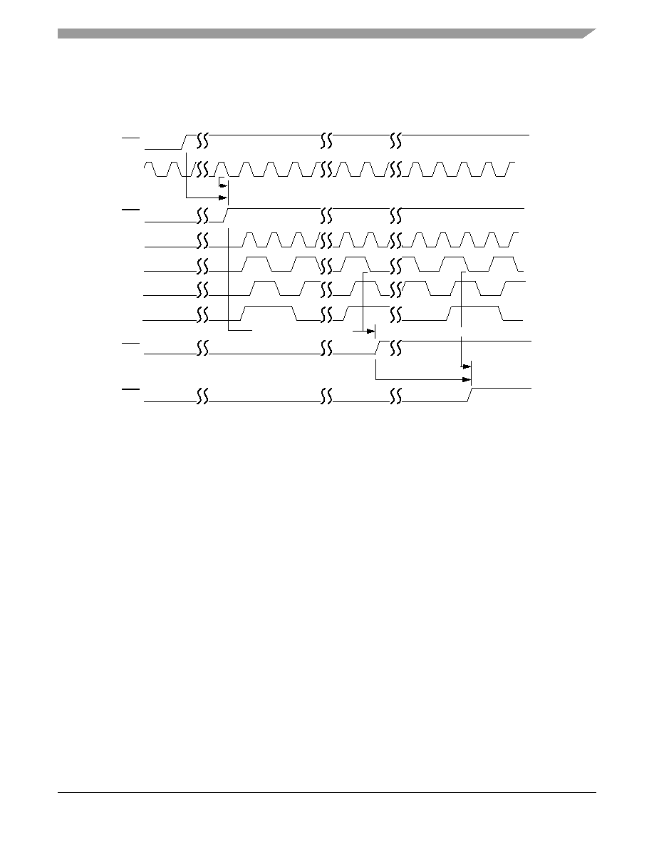
Interrupts
56F8013 Technical Data, Rev. 2
Freescale Semiconductor
81
Preliminary
Figure 6-16 Timing Relationships of Reset Signal to Clocks
6.8 Interrupts
The SIM generates no interrupts.
RST
MSTR_OSC
CKGEN_RST
SYS_CLK_x2
SYS_CLK
SYS_CLK_D
SYS_CLK_DIV2
PERIP_RST
CORE_RST
Switch on falling OSC_CLK
96 MSTR_OSC cycles
Switch on falling SYS_CLK
32 SYS_CLK cycles delay
32 SYS_CLK cycles delay
Maximum Delay = 64 MSTR_OSC cycles for POR reset extension and 32 MSTR_OSC cycles
for combined reset extension
Switch on falling SYS_CLK

56F8013 Technical Data, Rev. 2
82
Freescale Semiconductor
Preliminary
Part 7 Security Features
The 56F8013 offers security features intended to prevent unauthorized users from reading the contents of
the Flash Memory (FM) array. The 56F8013's Flash security consists of several hardware interlocks that
prevent unauthorized users from gaining access to the Flash array.
Note, however, that part of the security must lie with the user's code. An extreme example would be user's
code that includes a subroutine to read and transfer the contents of the internal program to SCI, SPI or
another peripheral, as this code would defeat the purpose of security. At the same time, the user may also
wish to put a "backdoor" in his program. As an example, the user downloads a security key through the
SCI, allowing access to a programming routine that updates parameters stored in another section of the
Flash.
7.1 Operation with Security Enabled
Once the user has programmed the Flash with his application code, the 56F8013 can be secured by
programming the security bytes located in the FM configuration field, which are located at the last 9 words
of Program Flash. These non-volatile bytes will keep the part secured through reset and through
power-down of the device. Only two bytes within this field are used to enable or disable security. Refer to
the Flash Memory chapter in the 56F8000 Peripheral User Manual for the state of the security bytes and
the resulting state of security. When Flash security mode is enabled in accordance with the method
described in the Flash Memory module chapter, the 56F8013 will disable the core EOnCE debug
capabilities. Normal program execution is otherwise unaffected.
7.2 Flash Access Lock and Unlock Mechanisms
The 56F8013 has several operating functional and debug modes. Effective Flash security must address
operating mode selection and anticipate modes in which the on-chip Flash can be read without explicit user
permission.
7.2.1
Disabling EOnCE Access
On-chip Flash can be read by issuing commands across the EOnCE port, which is the debug interface for
the 56800E CPU. The TCLK, TMS, TDO, and TDI pins comprise a JTAG interface onto which the
EOnCE port functionality is mapped. When the 56F8013 boots, the chip-level JTAG TAP (Test Access
Port) is active and provides the chip's boundary scan capability and access to the ID register, but proper
implementation of Flash security will block any attempt to access the internal Flash memory via the
EOnCE port when security is enabled.
7.2.2
Flash Lockout Recovery Using JTAG
If a user inadvertently enables security on the 56F8013, the only lockout recovery mechanism is the
complete erasure of the internal Flash contents, including the configuration field, and thus disables security
(the protection register is cleared). This does not compromise security, as the entire contents of the user's
secured code stored in Flash are erased before security is disabled on the 56F8013 on the next reset or
power-up sequence.

Flash Access Lock and Unlock Mechanisms
56F8013 Technical Data, Rev. 2
Freescale Semiconductor
83
Preliminary
To start the lockout recovery sequence, the JTAG public instruction (LOCKOUT_RECOVERY) must
first be shifted into the chip-level TAP controller's instruction register. Once the
LOCKOUT_RECOVERY instruction has been shifted into the instruction register, the clock divider value
must be shifted into the corresponding 7-bit data register. After the data register has been updated, the user
must transition the TAP controller into the RUN-TEST/IDLE state for the lockout sequence to commence.
The controller must remain in this state until the erase sequence has completed. Refer to the 56F8000
Peripheral User Manual for more details, or contact Freescale.
Note:
Once the lockout recovery sequence has completed, the user must reset both the JTAG TAP controller
(by advancing the TAP state machine to the reset state) and the 56F8013 (by asserting external chip
reset) to return to normal unsecured operation.
7.2.3
Flash Lockout Recovery using CodeWarrior
CodeWarrior can unlock a device using the command sequence described in Section 7.2.2 by selecting the
Debug menu, then selecting DSP56800E, followed by Unlock Flash.
Another mechanism is also built into CodeWarrior using the device's memory configuration file. The
command "Unlock_Flash_on_Connect1" in the .cfg file accomplishes the same task as using the Debug
menu.
7.2.4
Product Analysis
The recommended method of unsecuring a programmed 56F8013 for product analysis of field failures is
via the backdoor key access. The customer would need to supply Technical Support
with the backdoor key
and the protocol to access the backdoor routine in the Flash. Additionally, the KEYEN bit that allows
backdoor key access must be set.
An alternative method for performing analysis on a secured microcontroller would be to mass-erase and
reprogram the Flash with the original code, but modify the security bytes.
To insure that a customer does not inadvertently lock himself out of the 56F8013 during programming, it
is recommended that the user program the backdoor access key first, the application code second and the
security bytes within the FM configuration field last.

56F8013 Technical Data, Rev. 2
84
Freescale Semiconductor
Preliminary
Part 8 General Purpose Input/Output (GPIO)
8.1 Introduction
This section is intended to supplement the GPIO information found in the 56F8000 Peripheral User
Manual and contains only chip-specific information. This information supercedes the generic information
in the 56F8000 Peripheral User Manual.
8.2 Configuration
There are four GPIO ports defined on the 56F8013. The width of each port, the associated peripheral and
reset functions are shown in
Table 8-1
. The specific mapping of GPIO port pins is shown in
Table 8-2
.
Table 8-1 GPIO Ports Configuration
GPIO Port
Available
Pins in
56F8013
Peripheral Function
Reset Function
A
8
PWM, Reset
GPIO, except GPIOA7
B
8
SPI, SCI, Timer
GPIO
C
6
XTAL, EXTAL, CAN, TMRC (GPIOC5 and
GPIOC7 are not bonded out on the
56F8013)
Analog
D
4
JTAG
JTAG

Configuration
56F8013 Technical Data, Rev. 2
Freescale Semiconductor
85
Preliminary
Table 8-2 GPIO External Signals Map
Pins in shaded rows are not available in 56F8013
GPIO Function
Peripheral Function
LQFP
Package Pin
Notes
GPIOA0
PWM0
29
Defaults to A0
GPIOA1
PWM1
28
Defaults toA1
GPIOA2
PWM2
23
Defaults to A2
GPIOA3
PWM3
24
Defaults to A3
GPIOA4
PWM4 / FAULT1 / T2
22
SIM register SIM_GPS is used to
select between PWM4, FAULT1, and
T2
Defaults to A4
GPIOA5
PWM5 / FAULT2 / T3
20
SIM register SIM_GPS is used to
select between PWM5, FAULT2, and
T3
Defaults to A5
GPIOA6
FAULT0
18
Defaults to A6
GPIOA7
RESET
15
Defaults to RESET
GPIOB0
SCLK / SCL
21
SIM register SIM_GPS is used to
select between SCLK and SCL
Defaults to B0
GPIOB1
SS / SDA
2
SIM register SIM_GPS is used to
select between SS and SDA
Defaults to B1
GPIOB2
MISO / T2
17
SIM register SIM_GPS is used to
select between MISO and T2
Defaults to B2
GPIOB3
MOSI / T3
16
SIM register SIM_GPS is used to
select between MOSI and T3
Defaults to B3
GPIOB4
T0 / CLKO
19
SIM register SIM_GPS is used to
select between T0 and CLKO
Defaults to B4
GPIOB5
T1 / FAULT3
4
SIM register SIM_GPS is used to
select between T1 and FAULT3
Defaults to B5

56F8013 Technical Data, Rev. 2
86
Freescale Semiconductor
Preliminary
8.3 Reset Values
Tables
4-16
through
4-19
detail registers for the 56F8013; Figures
8-1
through
8-4
summarize register
maps and reset values.
GPIOB6
RXD / SDA / CLKIN
1
SIM register SIM_GPS is used to
select between RXD and SDA.
CLKIN functionality is enabled using
the PLL Control Register within the
OCCS block.
Defaults to B6
GPIOB7
TXD / SCL
3
SIM register SIM_GPS is used to
select between TXD and SCL
Defaults to B7
GPIOC0
ANA0
12
Defaults to ANA0
GPIOC1
ANA1
11
Defaults to ANA1
GPIOC2
ANA2 / V
REFH
10
Defaults to ANA2
GPIOC3
ANA3
Not bonded out in 56F8013
Defaults to ANA3
GPIOC4
ANB0
5
Defaults to ANB0
GPIOC5
ANB1
6
Defaults to ANB1
GPIOC6
ANB2 / V
REFL
7
Defaults to ANB2
GPIOC7
ANB3
Not bonded out in 56F8013
Defaults to ANB3
GPIOD0
TDI
30
Defaults to TDI
GPIOD1
TDO
32
Defaults to TDO
GPIOD2
TCK
14
Defaults to TCK
GPIOD3
TMS
31
Defaults to TMS
Table 8-2 GPIO External Signals Map (Continued)
Pins in shaded rows are not available in 56F8013
GPIO Function
Peripheral Function
LQFP
Package Pin
Notes

Reset Values
56F8013 Technical Data, Rev. 2
Freescale Semiconductor
87
Preliminary
Figure 8-1 GPIOA Register Map Summary
Add.
Offset
Register Acronym
15
14
13
12
11
10
9
8
7
6
5
4
3
2
1
0
$0
GPIOA_PUPEN
R
0
0
0
0
0
0
0
0
PU
W
RS
0
0
0
0
0
0
0
0
1
1
1
1
1
1
1
1
$1
GPIOA_DATA
R
0
0
0
0
0
0
0
0
D
W
RS
0
0
0
0
0
0
0
0
0
1
1
1
1
1
1
1
$2
GPIOA_DDIR
R
0
0
0
0
0
0
0
0
DD
W
RS
0
0
0
0
0
0
0
0
0
0
0
0
0
0
0
0
$3
GPIOA_PEREN
R
0
0
0
0
0
0
0
0
PE
W
RS
0
0
0
0
0
0
0
0
1
0
0
0
0
0
0
0
$4
GPIOA_IASSRT
R
0
0
0
0
0
0
0
0
IA
W
RS
0
0
0
0
0
0
0
0
0
0
0
0
0
0
0
0
$5
GPIOA_IEN
R
0
0
0
0
0
0
0
0
IEN
W
RS
0
0
0
0
0
0
0
0
0
0
0
0
0
0
0
0
$6
GPIOA_IEPOL
R
0
0
0
0
0
0
0
0
IEPOL
W
RS
0
0
0
0
0
0
0
0
0
0
0
0
0
0
0
0
$7
GPIOA_IPEND
R
0
0
0
0
0
0
0
0
IPR
W
RS
0
0
0
0
0
0
0
0
0
0
0
0
0
0
0
0
$8
GPIOA_IEDGE
R
0
0
0
0
0
0
0
0
IES
W
RS
0
0
0
0
0
0
0
0
0
0
0
0
0
0
0
0
$9
GPIOA_PPOUTM
R
0
0
0
0
0
0
0
0
OEN
W
RS
0
0
0
0
0
0
0
0
1
1
1
1
1
1
1
1
$A
GPIOA_RDATA
R
0
0
0
0
0
0
0
0
RAW DATA
W
RS
X
X
X
X
X
X
X
X
X
X
X
X
X
X
X
X
$B
GPIOA_DRIVE
R
0
0
0
0
0
0
0
0
DRIVE
W
RS
0
0
0
0
0
0
0
0
0
0
0
0
0
0
0
0
R
0
Read as 0
W
Reserved
RS
Reset

56F8013 Technical Data, Rev. 2
88
Freescale Semiconductor
Preliminary
Figure 8-2 GPIOB Register Map Summary
Add.
Offset
Register Acronym
15
14
13
12
11
10
9
8
7
6
5
4
3
2
1
0
$0
GPIOB_PUPEN
R
0
0
0
0
0
0
0
0
PU
W
RS
0
0
0
0
0
0
0
0
1
1
1
1
1
1
1
1
$1
GPIOB_DATA
R
0
0
0
0
0
0
0
0
D
W
RS
0
0
0
0
0
0
0
0
1
1
1
1
1
1
1
1
$2
GPIOB_DDIR
R
0
0
0
0
0
0
0
0
DD
W
RS
0
0
0
0
0
0
0
0
0
0
0
0
0
0
0
0
$3
GPIOB_PEREN
R
0
0
0
0
0
0
0
0
PE
W
RS
0
0
0
0
0
0
0
0
0
0
0
0
0
0
0
0
$4
GPIOB_IASSRT
R
0
0
0
0
0
0
0
0
IA
W
RS
0
0
0
0
0
0
0
0
0
0
0
0
0
0
0
0
$5
GPIOB_IEN
R
0
0
0
0
0
0
0
0
IEN
W
RS
0
0
0
0
0
0
0
0
0
0
0
0
0
0
0
0
$6
GPIOB_IEPOL
R
0
0
0
0
0
0
0
0
IEPOL
W
RS
0
0
0
0
0
0
0
0
0
0
0
0
0
0
0
0
$7
GPIOB_IPEND
R
0
0
0
0
0
0
0
0
IPR
W
RS
0
0
0
0
0
0
0
0
0
0
0
0
0
0
0
0
$8
GPIOB_IEDGE
R
0
0
0
0
0
0
0
0
IES
W
RS
0
0
0
0
0
0
0
0
0
0
0
0
0
0
0
0
$9
GPIOB_PPOUTM
R
0
0
0
0
0
0
0
0
OEN
W
RS
0
0
0
0
0
0
0
0
1
1
1
1
1
1
1
1
$A
GPIOB_RDATA
R
0
0
0
0
0
0
0
0
RAW DATA
W
RS
X
X
X
X
X
X
X
X
X
X
X
X
X
X
X
X
$B
GPIOB_DRIVE
R
0
0
0
0
0
0
0
0
DRIVE
W
RS
0
0
0
0
0
0
0
0
0
0
0
0
0
0
0
0
R
0
Read as 0
W
Reserved
RS
Reset
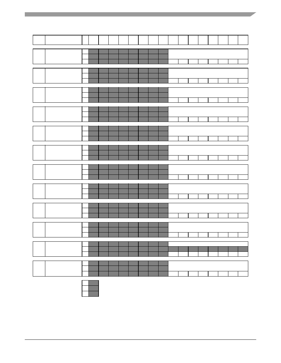
Reset Values
56F8013 Technical Data, Rev. 2
Freescale Semiconductor
89
Preliminary
Figure 8-3 GPIOC Register Map Summary
Add.
Offset
Register Acronym
15
14
13
12
11
10
9
8
7
6
5
4
3
2
1
0
$0
GPIOC_PUPEN
R
0
0
0
0
0
0
0
0
PU
W
RS
0
0
0
0
0
0
0
0
1
1
1
1
1
1
1
1
$1
GPIOC_DATA
R
0
0
0
0
0
0
0
0
D
W
RS
0
0
0
0
0
0
0
0
0
0
0
0
0
0
0
0
$2
GPIOC_DDIR
R
0
0
0
0
0
0
0
0
DD
W
RS
0
0
0
0
0
0
0
0
0
0
0
0
0
0
0
0
$3
GPIOC_PEREN
R
0
0
0
0
0
0
0
0
PE
W
RS
0
0
0
0
0
0
0
0
1
1
1
1
1
1
1
1
$4
GPIOC_IASSRT
R
0
0
0
0
0
0
0
0
IA
W
RS
0
0
0
0
0
0
0
0
0
0
0
0
0
0
0
0
$5
GPIOC_IEN
R
0
0
0
0
0
0
0
0
IEN
W
RS
0
0
0
0
0
0
0
0
0
0
0
0
0
0
0
0
$6
GPIOC_IEPOL
R
0
0
0
0
0
0
0
0
IEPOL
W
RS
0
0
0
0
0
0
0
0
0
0
0
0
0
0
0
0
$7
GPIOC_IPEND
R
0
0
0
0
0
0
0
0
IPR
W
RS
0
0
0
0
0
0
0
0
0
0
0
0
0
0
0
0
$8
GPIOC_IEDGE
R
0
0
0
0
0
0
0
0
IES
W
RS
0
0
0
0
0
0
0
0
0
0
0
0
0
0
0
0
$9
GPIOC_PPOUTM
R
0
0
0
0
0
0
0
0
OEN
W
RS
0
0
0
0
0
0
0
0
1
1
1
1
1
1
1
1
$A
GPIOC_RDATA
R
0
0
0
0
0
0
0
0
RAW DATA
W
RS
X
X
X
X
X
X
X
X
X
X
X
X
X
X
X
X
$B
GPIOC_DRIVE
R
0
0
0
0
0
0
0
0
DRIVE
W
RS
0
0
0
0
0
0
0
0
0
0
0
0
0
0
0
0
R
0
Read as 0
W
Reserved
RS
Reset

56F8013 Technical Data, Rev. 2
90
Freescale Semiconductor
Preliminary
Figure 8-4 GPIOD Register Map Summary
Add.
Offset
Register Acronym
15
14
13
12
11
10
9
8
7
6
5
4
3
2
1
0
$0
GPIOD_PUPEN
R
0
0
0
0
0
0
0
0
0
0
0
0
PU
W
RS
0
0
0
0
0
0
0
0
0
0
0
0
1
1
1
1
$1
GPIOD_DATA
R
0
0
0
0
0
0
0
0
0
0
0
0
D
W
RS
0
0
0
0
0
0
0
0
0
0
0
0
0
0
0
0
$2
GPIOD_DDIR
R
0
0
0
0
0
0
0
0
0
0
0
0
DD
W
RS
0
0
0
0
0
0
0
0
0
0
0
0
0
0
0
0
$3
GPIOD_PEREN
R
0
0
0
0
0
0
0
0
0
0
0
0
PE
W
RS
0
0
0
0
0
0
0
0
0
0
0
0
1
1
1
1
$4
GPIOD_IASSRT
R
0
0
0
0
0
0
0
0
0
0
0
0
IA
W
RS
0
0
0
0
0
0
0
0
0
0
0
0
0
0
0
0
$5
GPIOD_IEN
R
0
0
0
0
0
0
0
0
0
0
0
0
IEN
W
RS
0
0
0
0
0
0
0
0
0
0
0
0
0
0
0
0
$6
GPIOD_IEPOL
R
0
0
0
0
0
0
0
0
0
0
0
0
IEPOL
W
RS
0
0
0
0
0
0
0
0
0
0
0
0
0
0
0
0
$7
GPIOD_IPEND
R
0
0
0
0
0
0
0
0
0
0
0
0
IPR
W
RS
0
0
0
0
0
0
0
0
0
0
0
0
0
0
0
0
$8
GPIOD_IEDGE
R
0
0
0
0
0
0
0
0
0
0
0
0
IES
W
RS
0
0
0
0
0
0
0
0
0
0
0
0
0
0
0
0
$9
GPIOD_PPOUTM
R
0
0
0
0
0
0
0
0
0
0
0
0
OEN
W
RS
0
0
0
0
0
0
0
0
0
0
0
0
1
1
1
1
$A
GPIOD_RDATA
R
0
0
0
0
0
0
0
0
0
0
0
0
RAW DATA
W
RS
X
X
X
X
X
X
X
X
X
X
X
X
X
X
X
X
$B
GPIOD_DRIVE
R
0
0
0
0
0
0
0
0
0
0
0
0
DRIVE
W
RS
0
0
0
0
0
0
0
0
0
0
0
0
0
0
0
0
R
0
Read as 0
W
Reserved
RS
Reset

56F8013 Information
56F8013 Technical Data, Rev. 2
Freescale Semiconductor
91
Preliminary
Part 9 Joint Test Action Group (JTAG)
9.1 56F8013 Information
Please contact your Freescale sales representative or authorized distributor for device/package-specific
BSDL information.
The TRST pin is not available in this package. The pin is tied to V
DD
in the package.
The JTAG state machine is reset during POR and can also be reset via a soft reset by holding TMS high
for five rising edges of TCK, as described in the 56F8000 Peripheral User Manual.
Part 10 Specifications
10.1 General Characteristics
The 56F8013 is fabricated in high-density CMOS with 5V-tolerant TTL-compatible digital inputs. The
term "5V-tolerant" refers to the capability of an I/O pin, built on a 3.3V-compatible process technology,
to withstand a voltage up to 5.5V without damaging the device. Many systems have a mixture of devices
designed for 3.3V and 5V power supplies. In such systems, a bus may carry both 3.3V- and 5V-compatible
I/O voltage levels (a standard 3.3V I/O is designed to receive a maximum voltage of 3.3V
± 10% during
normal operation without causing damage). This 5V-tolerant capability therefore offers the power savings
of 3.3V I/O levels, combined with the ability to receive 5V levels without damage.
Absolute maximum ratings in
Table 10-1
are stress ratings only, and functional operation at the maximum
is not guaranteed. Stress beyond these ratings may affect device reliability or cause permanent damage to
the device.
Unless otherwise stated, all specifications within this chapter apply over the temperature range of -40∫C to
105∫C ambient temperature over the following supply ranges:
V
SS
= V
SS
A = 0V, V
DD
= V
DDA
= 3.0≠3.6V, CL < 50pF, f
OP
= 32MHz
CAUTION
This device contains protective circuitry to guard
against damage due to high static voltage or electrical
fields. However, normal precautions are advised to
avoid application of any voltages higher than
maximum-rated voltages to this high-impedance circuit.
Reliability of operation is enhanced if unused inputs are
tied to an appropriate voltage level.

56F8013 Technical Data, Rev. 2
92
Freescale Semiconductor
Preliminary
Default Mode
Pin Group 1: GPIO, TDI, TDO, TMS, TCK
Pin Group 2: RESET, GPIOA7
Pin Group 3: ADC Analog Inputs
Table 10-1 Absolute Maximum Ratings
(V
SS
= 0V, V
SSA
= 0V)
Characteristic
Symbol
Notes
Min
Max
Unit
Supply Voltage Range
V
DD
-0.3
4.0
V
Analog Supply Voltage Range
V
DDA
- 0.3
4.0
V
ADC High Voltage Reference
V
REFH
- 0.3
4.0
V
Input Voltage Range (Digital inputs)
V
IN
Pin Groups 1, 2
- 0.3
6.0
V
Input Voltage Range (ADC inputs)
V
INA
Pin Group 3
- 0.3
4.0
V
Input clamp current, per pin (V
IN
< 0)
1
1. Continuous input current per pin is -2 mA
V
IC
-
-20
mA
Output clamp current, per pin (V
O
< 0)
1
V
OC
-
-20
mA
Output Voltage Range
(Normal Push-Pull mode)
V
OUT
Pin Group 1
-0.3
4.0
V
Output Voltage Range
(Open Drain mode)
V
OUTOD
Pin Groups 1, 2
-0.3
6.0
V
Ambient Temperature
T
A
-40
105
∞C
Storage Temperature Range
T
S
-55
150
∞C

General Characteristics
56F8013 Technical Data, Rev. 2
Freescale Semiconductor
93
Preliminary
10.1.1 ElectroStatic Discharge (ESD) Model
1. Junction temperature is a function of die size, on-chip power dissipation, package thermal resistance, mounting site (board)
temperature, ambient temperature, air flow, power dissipation of other components on the board, and board thermal resistance.
2. Per SEMI G38-87 and JEDEC JESD51-2 with the single layer board horizontal.
3. Per JEDEC JESC51-6 with the board horizontal.
4. Thermal resistance between the die and the printed circuit board per JEDEC JESD51-8. Board temperature is
measured on the top surface of the board near the package.
5. Thermal resistance between the die and the case top surface as measured by the cold plate method (MIL SPEC-883 Method
1012.1).
6. Thermal characterization parameter indicating the temperature difference between package top and the junction temperature per
JEDEC JESD51-2. When Greek letters are not available, the thermal characterization parameter is written as Psi-JT.
7. See
Section 12.1
for more details on thermal design considerations.
Table 10-2 56F8013 ESD Protection
Characteristic
Min
Typ
Max
Unit
ESD for Human Body Model (HBM)
2000
--
--
V
ESD for Machine Model (MM)
200
--
--
V
ESD for Charge Device Model (CDM)
750
--
--
V
Table 10-3 LQFP Package Thermal Characteristics
6
Characteristic
Comments
Symbol
Value
(LQFP)
Unit
Notes
Junction to ambient
Natural convection
Single layer board
(1s)
R
JA
74
∞C/W
1,2
Junction to ambient
Natural convection
Four layer board
(2s2p)
R
JMA
50
∞C/W
1,3
Junction to ambient
(@200 ft/min)
Single layer board
(1s)
R
JMA
67
∞C/W
1,3
Junction to ambient
(@200 ft/min)
Four layer board
(2s2p)
R
JMA
46
∞C/W
1,3
Junction to board
R
JB
23
∞C/W
4
Junction to case
R
JC
20
∞C/W
5
Junction to package top
Natural Convection
JT
4
∞C/W
6

56F8013 Technical Data, Rev. 2
94
Freescale Semiconductor
Preliminary
Note: Total chip source or sink current cannot exceed 50mA
Default Mode
Pin Group 1: GPIO, TDI, TDO, TMS, TCK
Pin Group 2: RESET, GPIOA7
Pin Group 3: ADC analog inputs
Table 10-4 Recommended Operating Conditions
(V
REFL
= 0V, V
SSA
= 0V, V
SS
= 0V
)
Characteristic
Symbol
Notes
Min
Typ
Max
Unit
Supply voltage
V
DD
3
3.3
3.6
V
ADC Supply voltage
V
DDA
3
3.3
3.6
V
ADC High Voltage Reference
V
REFH
3
--
V
DDA
V
Device Clock Frequency
Using relaxation oscillator
Using external clock source
FSYSCLK
8
0
--
32
32
MHz
Input Voltage High (digital inputs)
V
IH
Pin Groups 1, 2
2
--
5.5
V
Input Voltage Low (digital inputs)
V
IL
Pin Groups 1, 2
-0.3
--
0.8
V
Output Source Current High
(at V
OH
min.)
When programmed for low drive
strength
When programmed for high drive
strength
I
OH
Pin Group 1
Pin Group 1
--
--
--
--
-4
-8
mA
Output Source Current Low
(at V
OL
max.)
When programmed for low drive
strength
When programmed for high drive
strength
I
OL
Pin Groups 1, 2
Pin Groups 1, 2
--
--
--
--
4
8
mA
Ambient Operating Temperature
T
A
-40
--
105 -
(R
JA
X P
D
)
∞C
Flash Endurance
(Program Erase Cycles)
N
F
T
A
= -40∞C
to 105∞C
10,000
--
--
Cycles
Flash Data Retention
T
R
T
J
<= 70∞C
avg
15
--
--
Years

DC Electrical Characteristics
56F8013 Technical Data, Rev. 2
Freescale Semiconductor
95
Preliminary
10.2 DC Electrical Characteristics
(a) See
Figure 10-1
Default Mode
Pin Group 1: GPIO, TDI, TDO, TMS, TCK
Pin Group 2: RESET, GPIOA7
Pin Group 3: ADC Analog Inputs
Figure 10-1 I
IN
/I
OZ
vs. Voltage (Typical)
Table 10-5 DC Electrical Characteristics
At Recommended Operating Conditions
Characteristic
Symbol
Notes
Min
Typ
Max
Unit
Test
Conditions
Output Voltage High
V
OH
Pin Group 1
2.4
--
--
V
I
OH
= I
OHmax
Output Voltage Low
V
OL
Pin Groups 1, 2
--
--
0.4
V
I
OL
= I
OLmax
Digital Input Current High (a)
pull-up enabled or disabled
I
IH
Pin Groups 1, 2
--
0
+/- 2.5
µ
A
V
IN
= 2.4V
to 5.5V
ADC Input Current High
I
IHA
Pin Group 3
--
0
+/- 10
µ
A
V
INA
= V
DDA
Digital Input Current Low (a)
pull-up enabled
pull-up disabled
I
IL
Pin Groups 1, 2
-15
--
-30
-60
+/- 2.5
µ
A
V
IN
= 0V
ADC Input Current Low
I
ILA
Pin Group 3
--
0
+/- 10
µ
A
V
INA
= 0V
Output Current
High Impedance State (a)
I
OZ
Pin Groups 1, 2
--
0
+/- 2.5
µ
A
V
OUT
= 2.4V
to 5.5V or
0V
Schmitt Trigger Input Hysteresis
V
HYS
Pin Groups 1, 2
--
0.35
--
V
--
Input Capacitance
C
IN
--
10
--
pF
--
Output Capacitance
C
OUT
--
10
--
pF
--
2.0
0.0
- 2.0
- 4.0
- 6.0
- 8.0
- 10.0
0.0
0.5
1.0
1.5
2.0
2.5
3.0
6.0
3.5
4.0
4.5
5.0
5.5
µA
Volt

56F8013 Technical Data, Rev. 2
96
Freescale Semiconductor
Preliminary
Table 10-6 Current Consumption per Power Supply Pin (Typical)
Mode
Conditions
I
DD
1
1. No Output Switching
All ports configured as inputs
All inputs Low
No DC Loads
I
DDA
RUN
32MHz Device Clock
Relaxation Oscillator on
PLL powered on
Continuous MAC instructions with fetches from Program Flash
All peripheral modules enabled. TMR and PWM using 1x Clock
ADC powered on and clocked
42mA
13.5mA
WAIT
32MHz Device Clock
Relaxation Oscillator on
PLL powered on
Core halted
All Peripheral modules enabled. TMR and PWM using 1x Clock
ADC powered off
17mA
0
µ
A
STOP
8MHz Device Clock
Relaxation Oscillator on
PLL powered off
All peripheral module and core clocks are off
ADC powered off
5mA
0µ
A
STANDBY
100KHz Device Clock
Relaxation Oscillator in Standby mode
PLL powered off
All peripheral module and core clocks are off
ADC in Standby mode
Voltage Regulator in Standby mode
210
µ
A
400
µ
A
STANDBY > STOP
100KHz Device Clock
Relaxation Oscillator in Standby mode
PLL powered off
All peripheral module and core clocks are off
ADC powered off
Voltage regulator in Standby mode
210
µ
A
0
µ
A
POWERDOWN
Device Clock is off
Relaxation Oscillator powered off
PLL powered off
All peripheral module and core clocks are off
ADC powered off
Voltage Regulator in Standby mode
160
µ
A
0
µ
A
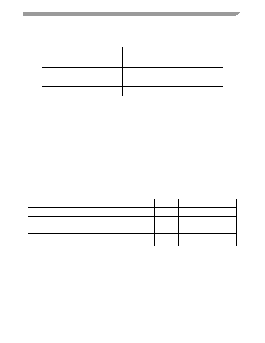
DC Electrical Characteristics
56F8013 Technical Data, Rev. 2
Freescale Semiconductor
97
Preliminary
10.2.1 Voltage Regulator Specifications
The 56F8013 has two on-chip regulators. One supplies the PLL and relaxation oscillator. It has no external
pins and therefore has no external characteristics which must be guaranteed (other than proper operation
of the device). The second regulator supplies approximately 2.5V to the 56F8013's core logic. This
regulator requires an external 4.4
µ
F, or greater, capacitor for proper operation. Ceramic and tantalum
capacitors tend to provide better performance tolerances. The output voltage can be measured directly on
the V
CAP
pin. The specifications for this regulator are shown in
Table 10-8
.
Table 10-7 Power-On Reset Low-Voltage Parameters
Characteristic
Symbol
Min
Typ
Max
Unit
Low-Voltage Interrupt for 3.3V supply
1
1. When V
DD
drops below V
EI3.3
maximum value, an interrupt is generated.
V
EI3.3
2.65
2.7
--
V
Low-Voltage Interrupt for 2.5V supply
2
2. When V
DD
drops below V
EI32.5
maximum value, an interrupt is generated.
V
E12.5
2.05
2.15
--
V
Low-Voltage Interrupt Recovery Hysteresis
V
EIH
--
50
--
mV
Power-On Reset
3
3. Power-On Reset occurs whenever the internally regulated 2.5V digital supply drops below 1.8V. While
power is ramping up, this signal remains active for as long as the internal 2.5V is below 2.15V or the 3.3V
1/O voltage is below 2.7V, no matter how long the ramp-up rate is. The internally regulated voltage is
typically 100mV less than V
DD
during ramp-up until 2.5V is reached, at which time it self-regulates.
POR
--
1.8
1.9
V
Table 10-8. Regulator Parameters
Characteristic
Symbol
Min
Typical
Max
Unit
Input Voltage
V
IN
3.0
--
3.6
V
Output Voltage
V
OUT
2.25
2.5
2.75
V
Short Circuit Current
I
SS
--
450
650
mA
Short Circuit Tolerance
(output shorted to ground)
T
RSC
--
--
30
Minutes

56F8013 Technical Data, Rev. 2
98
Freescale Semiconductor
Preliminary
10.3 AC Electrical Characteristics
Tests are conducted using the input levels specified in
Table 10-5
. Unless otherwise specified,
propagation delays are measured from the 50% to the 50% point, and rise and fall times are measured
between the 10% and 90% points, as shown in
Figure 10-2
.
Figure 10-2 Input Signal Measurement References
Figure 10-3
shows the definitions of the following signal states:
∑
Active state, when a bus or signal is driven, and enters a low impedance state
∑
Tri-stated, when a bus or signal is placed in a high impedance state
∑
Data Valid state, when a signal level has reached V
OL
or V
OH
∑
Data Invalid state, when a signal level is in transition between V
OL
and V
OH
Figure 10-3 Signal States
10.4 Flash Memory Characteristics
Table 10-9 Flash Timing Parameters
Characteristic
Symbol
Min Typ
Max Unit
Program time
1
1. There is additional overhead which is part of the programming sequence. See the 56F8000 Peripheral User Manual
for details. Program time is per 16-bit word in Flash memory. Two words at a time can be programmed within the Pro-
gram Flash Module, as it contains two interleaved memories.
T
prog
20
--
40
µ
s
Erase time
2
2. Specifies page erase time. There are 512 bytes per page in the Program Flash memory. The Program Flash Module
uses two interleaved Flash memories, increasing the effective page size to 1024 bytes.
T
erase
20
--
--
ms
Mass erase time
T
me
100
--
--
ms
V
IH
V
IL
Fall Time
Input Signal
Note: The midpoint is V
IL
+ (V
IH
≠ V
IL
)/2.
Midpoint1
Low
High
90%
50%
10%
Rise Time
Data Invalid State
Data1
Data2 Valid
Data
Tri-stated
Data3 Valid
Data2
Data3
Data1 Valid
Data Active
Data Active
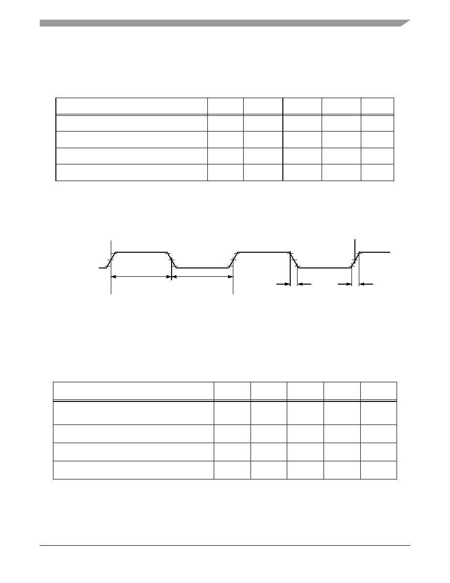
External Clock Operation Timing
56F8013 Technical Data, Rev. 2
Freescale Semiconductor
99
Preliminary
10.5 External Clock Operation Timing
Figure 10-4 External Clock Timing
10.6 Phase Locked Loop Timing
Table 10-10 External Clock Operation Timing Requirements
1
1. Parameters listed are guaranteed by design.
Characteristic
Symbol
Min
Typ
Max
Unit
Frequency of operation (external clock driver)
2
2. See
Figure 10-4
for details on using the recommended connection of an external clock driver.
f
osc
4
8
8
MHz
Clock Pulse Width
3
3. The high or low pulse width must be no smaller than 6.25ns or the chip may not function.
t
PW
6.25
--
--
ns
External Clock Input Rise Time
4
4. External clock input rise time is measured from 10% to 90%.
t
rise
--
--
3
ns
External Clock Input Fall Time
5
5. External clock input fall time is measured from 90% to 10%.
t
fall
--
--
3
ns
Table 10-11 PLL Timing
Characteristic
Symbol
Min
Typ
Max
Unit
Internal reference relaxation oscillator frequency for
the PLL
f
rosc
--
8
--
MHz
PLL output frequency
1
(24 x reference frequency)
1. The core system clock will operate at 1/6 of the PLL output frequency.
f
op
--
192
--
MHz
PLL lock time
2
2. This is the time required after the PLL is enabled to ensure reliable operation.
t
lock
--
.1
1
ms
Cycle-to-cycle jitter
t
jitterpll
350
ps
External
Clock
V
IH
V
IL
Note: The midpoint is V
IL
+ (V
IH
≠ V
IL
)/2.
90%
50%
10%
90%
50%
10%
t
PW
t
PW
t
fall
t
rise

56F8013 Technical Data, Rev. 2
100
Freescale Semiconductor
Preliminary
10.7 Relaxation Oscillator Timing
Figure 10-5 Relaxation Oscillator Temperature Variation (Typical)
Table 10-12 Relaxation Oscillator Timing
Characteristic
Symbol
Minimum
Typical
Maximum
Unit
Relaxation Oscillator output frequency
1
Normal Mode
Standby Mode
1. Output frequency after application of trim value, at 25∞C.
f
op
--
8
400
--
MHz
kHz
Relaxation Oscillator stabilization time
2
2. This is the time required from standby to normal mode transition.
t
roscs
--
1
3
µs
Cycle-to-cycle jitter. This is measured on the
CLKO signal (programmed prescaler_clock)
over 264 clocks
3
3. J
A
is required to meet SCI requirements.
t
jitterrosc
--
400
ps
Minimum tuning step size
.08
%
Maximum tuning step size
40
%
Variation over temperature -40
∞
C to 105
∞
C
4
4. See
Figure 10-5
.
--
+3.0 to -3.0
%
8.05
8
7.95
7.9
7.85
7.8
175
-25
-50
0
50
75
100
125
150
25
Degrees C (Junction)
MHz

Reset, Stop, Wait, Mode Select, and Interrupt Timing
56F8013 Technical Data, Rev. 2
Freescale Semiconductor
101
Preliminary
10.8 Reset, Stop, Wait, Mode Select, and Interrupt Timing
Note: All the address and data buses described here are internal.
Figure 10-6 GPIO Interrupt Timing (Negative Edge-Sensitive)
Table 10-13 Reset, Stop, Wait, Mode Select, and Interrupt Timing
1,2
1. In the formulas, T = clock cycle and T
osc
= oscillator clock cycle. For an operating frequency of 32MHz, T = 31.25ns. At 8MHz
(used during Reset and Stop modes), T = 125ns.
2. Parameters listed are guaranteed by design.
Characteristic
Symbol
Typical Min
Typical Max
Unit
See Figure
Minimum RESET Assertion Duration
t
RA
4T
--
ns
Minimum GPIO pin Assertion for Interrupt
t
IW
2T
--
ns
10-6
RESET deassertion to First Address Fetch
3
3. During Power-On Reset, it is possible to use the 56F8013 internal reset stretching circuitry to extend this period to 2^21T.
t
RDA
96T
OSC
+ 64T
97T
OSC
+ 65T
ns
Delay from Interrupt Assertion to Fetch of first
instruction (exiting Stop)
t
IF
--
6T
ns
GPIO pin
(Input)
T
IW

56F8013 Technical Data, Rev. 2
102
Freescale Semiconductor
Preliminary
10.9 Serial Peripheral Interface (SPI) Timing
Table 10-14 SPI Timing
1
1. Parameters listed are guaranteed by design.
Characteristic
Symbol
Min
Max
Unit
See Figure
Cycle time
Master
Slave
t
C
125
62.5
--
--
ns
ns
10-7
,
10-8
,
10-9
,
10-10
Enable lead time
Master
Slave
t
ELD
--
31
--
--
ns
ns
10-10
Enable lag time
Master
Slave
t
ELG
--
125
--
--
ns
ns
10-10
Clock (SCK) high time
Master
Slave
t
CH
50
31
--
--
ns
ns
10-7
,
10-8
,
10-9
,
10-10
Clock (SCK) low time
Master
Slave
t
CL
50
31
--
--
ns
ns
10-10
Data set-up time required for inputs
Master
Slave
t
DS
20
0
--
--
ns
ns
10-7
,
10-8
,
10-9
,
10-10
Data hold time required for inputs
Master
Slave
t
DH
0
2
--
--
ns
ns
10-7
,
10-8
,
10-9
,
10-10
Access time (time to data active from
high-impedance state)
Slave
t
A
4.8
15
ns
10-10
Disable time (hold time to high-impedance state)
Slave
t
D
3.7
15.2
ns
10-10
Data Valid for outputs
Master
Slave (after enable edge)
t
DV
--
--
4.5
20.4
ns
ns
10-7
,
10-8
,
10-9
,
10-10
Data invalid
Master
Slave
t
DI
0
0
--
--
ns
ns
10-7
,
10-8
,
10-9
,
10-10
Rise time
Master
Slave
t
R
--
--
11.5
10.0
ns
ns
10-7
,
10-8
,
10-9
,
10-10
Fall time
Master
Slave
t
F
--
--
9.7
9.0
ns
ns
10-7
,
10-8
,
10-9
,
10-10

Serial Peripheral Interface (SPI) Timing
56F8013 Technical Data, Rev. 2
Freescale Semiconductor
103
Preliminary
1
Figure 10-7 SPI Master Timing (CPHA = 0)
Figure 10-8 SPI Master Timing (CPHA = 1)
SCLK (CPOL = 0)
(Output)
SCLK (CPOL = 1)
(Output)
MISO
(Input)
MOSI
(Output)
MSB in
Bits 14≠1
LSB in
t
F
t
C
t
CL
t
CL
t
R
t
R
t
F
t
DS
t
DH
t
CH
t
DI
t
DV
t
DI
(ref)
t
R
Master MSB out
Bits 14≠1
Master LSB out
SS
(Input)
t
CH
SS is held High on master
t
F
SCLK (CPOL = 0)
(Output)
SCLK (CPOL = 1)
(Output)
MISO
(Input)
MOSI
(Output)
MSB in
Bits 14≠1
LSB in
t
R
t
C
t
CL
t
CL
t
F
t
CH
t
DV
(ref)
t
DV
t
DI
(ref)
t
R
t
F
Master MSB out
Bits 14≠ 1
Master LSB out
SS
(Input)
t
CH
SS is held High on master
t
DS
t
DH
t
DI
t
R
t
F
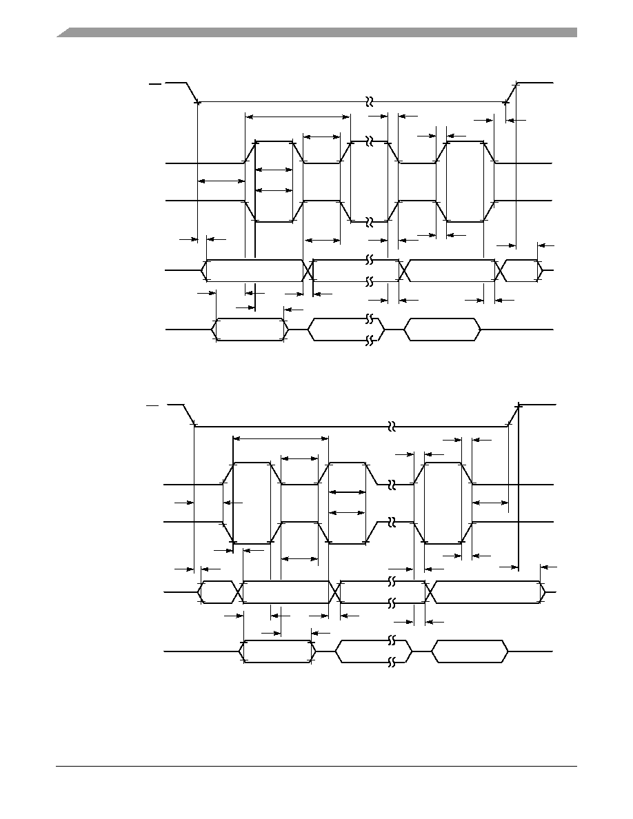
56F8013 Technical Data, Rev. 2
104
Freescale Semiconductor
Preliminary
Figure 10-9 SPI Slave Timing (CPHA = 0)
Figure 10-10 SPI Slave Timing (CPHA = 1)
SCLK (CPOL = 0)
(Input)
SCLK (CPOL = 1)
(Input)
MISO
(Output)
MOSI
(Input)
Slave MSB out
Bits 14≠1
t
C
t
CL
t
CL
t
F
t
CH
t
DI
MSB in
Bits 14≠1
LSB in
SS
(Input)
t
CH
t
DH
t
R
t
ELG
t
ELD
t
F
Slave LSB out
t
D
t
A
t
DS
t
DV
t
DI
t
R
SCLK (CPOL = 0)
(Input)
SCLK (CPOL = 1)
(Input)
MISO
(Output)
MOSI
(Input)
Slave MSB out
Bits 14≠1
t
C
t
CL
t
CL
t
CH
t
DI
MSB in
Bits 14≠1
LSB in
SS
(Input)
t
CH
t
DH
t
F
t
R
Slave LSB out
t
D
t
A
t
ELD
t
DV
t
F
t
R
t
ELG
t
DV
t
DS

Quad Timer Timing
56F8013 Technical Data, Rev. 2
Freescale Semiconductor
105
Preliminary
10.10 Quad Timer Timing
Figure 10-11 Timer Timing
Table 10-15 Timer Timing
1, 2
1. In the formulas listed, T = the clock cycle. For 32MHz operation, T = 31.25ns.
2. Parameters listed are guaranteed by design.
Characteristic
Symbol
Min
Max
Unit
See Figure
Timer input period
P
IN
2T + 6
--
ns
10-11
Timer input high / low period
P
INHL
1T + 3
--
ns
10-11
Timer output period
P
OUT
125
--
ns
10-11
Timer output high / low period
P
OUTHL
50
--
ns
10-11
P
OUT
P
OUTHL
P
OUTHL
P
IN
P
INHL
P
INHL
Timer Inputs
Timer Outputs
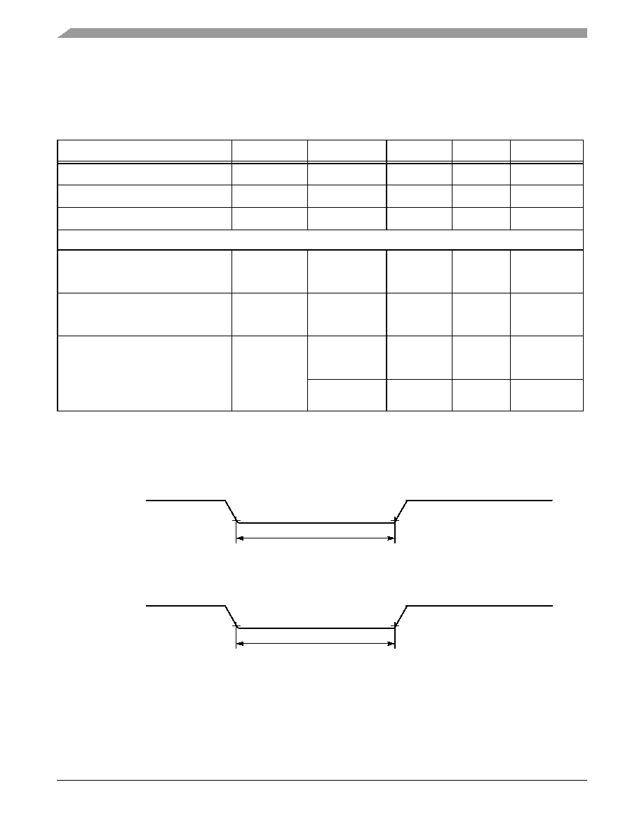
56F8013 Technical Data, Rev. 2
106
Freescale Semiconductor
Preliminary
10.11 Serial Communication Interface (SCI) Timing
Figure 10-12 RXD Pulse Width
Figure 10-13 TXD Pulse Width
Table 10-16 SCI Timing
1
1. Parameters listed are guaranteed by design.
Characteristic
Symbol
Min
Max
Unit
See Figure
Baud Rate
2
2. f
MAX
is the frequency of operation of the system clock in MHz, which is 32MHz for the 56F8013 device.
BR
--
(f
MAX
/16)
Mbps
--
RXD
3
Pulse Width
3. The RXD pin in SCI0 is named RXD0 and the RXD pin in SCI1 is named RXD1.
RXD
PW
0.965/BR
1.04/BR
ns
10-12
TXD
4
Pulse Width
4. The TXD pin in SCI0 is named TXD0 and the TXD pin in SCI1 is named TXD1.
TXD
PW
0.965/BR
1.04/BR
ns
10-13
LIN Slave Mode
Deviation of slave node clock from
nominal clock rate before
synchronization
F
TOL_UNSYNCH
-14
14
%
Deviation of slave node clock relative
to the master node clock after
synchronization
F
TOL_SYNCH
-2
2
%
Minimum break character length
T
BREAK
13
Master
node bit
periods
11
Slave node
bit periods
RXD
PW
RXD
Receive
data pin
(Input)
TXD
PW
TXD
Receive
data pin
(Input)

Inter-Integrated Circuit Interface (I2C) Timing
56F8013 Technical Data, Rev. 2
Freescale Semiconductor
107
Preliminary
10.12 Inter-Integrated Circuit Interface (I
2
C) Timing
Table 10-17 I
2
C Timing
Characteristic
Symbol
Standard Mode
Fast Mode
Unit
Minimum
Maximum
Minimum
Maximum
SCL Clock Frequency
f
SCL
0
100
0
400
kHz
Hold time (repeated )
START condition. After
this period, the first clock
pulse is generated.
t
HD; STA
4.0
0.6
µ
s
LOW period of the SCL
clock
t
LOW
4.7
1.25
µ
s
HIGH period of the SCL
clock
t
HIGH
4.0
0.6
µ
s
Set-up time for a repeated
START condition
t
SU; STA
4.7
0.6
µ
s
Data hold time for I
2
C bus
devices
t
HD; DAT
0
1
1. A device must internally provide a hold time of at least 300ns for the SDA signal (referred to the V
IH
min of the SCL
signal) to bridge the undefined region of the falling edge of SCL.
3.45
2
2. The maximum t
HD;
DAT
has only to be met if the device does not stretch the LOW period (t
LOW
) of the SCL signal.
0
1
0.9
2
µ
s
Data set-up time
t
SU; DAT
250
100
3
3. A Fast mode I
2
C bus device can be used in a Standard mode I
2
C bus system, but the requirement t
SU; DAT
> = 250ns
must then be met. This will automatically be the case if the device does not stretch the LOW period of the SCL signal.
If such a device does stretch the LOW period of the SCL signal, it must output the next data bit to the SDA line
t
rmax
+ t
SU; DAT
= 1000 + 250 = 1250ns (according to the Standard mode I
2
C bus specification) before the SCL line is
released.
ns
Rise time of both SDA and
SCL signals
t
r
1000
2 +0.1C
b
4
4. C
b
= total capacitance of the one bus line in pF.
300
ns
Fall time of both SDA and
SCL signals
t
f
300
2 +0.1C
b
4
300
ns
Set-up time for STOP
condition
t
SU; STO
4.0
0.6
µ
s
Bus free time between
STOP and START
condition
t
BUF
4.7
1.3
µ
s
Pulse width of spikes that
must be suppressed by
the input filter
t
SP
N/A
N/A
0.0
50
ns
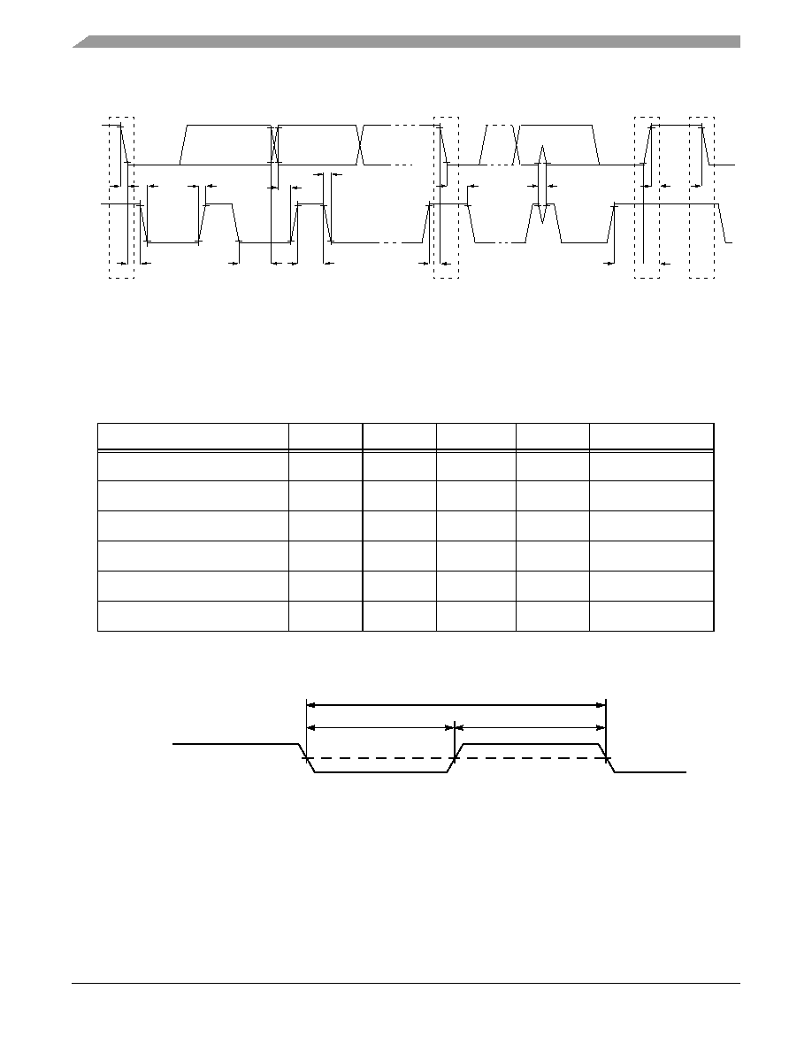
56F8013 Technical Data, Rev. 2
108
Freescale Semiconductor
Preliminary
Figure 10-14 Timing Definition for Fast and Standard Mode Devices on the I
2
C Bus
10.13 JTAG Timing
Figure 10-15 Test Clock Input Timing Diagram
Table 10-18 JTAG Timing
Characteristic
Symbol
Min
Max
Unit
See Figure
TCK frequency of operation
1
1. TCK frequency of operation must be less than 1/8 the processor rate.
f
OP
DC
SYS_CLK/8
MHz
10-15
TCK clock pulse width
t
PW
50
--
ns
10-15
TMS, TDI data set-up time
t
DS
5
--
ns
10-16
TMS, TDI data hold time
t
DH
5
--
ns
10-16
TCK low to TDO data valid
t
DV
--
30
ns
10-16
TCK low to TDO tri-state
t
TS
--
30
ns
10-16
SDA
SCL
t
HD; STA
t
HD; DAT
t
LOW
t
SU; DAT
t
HIGH
t
SU; STA
BR
P
S
S
t
HD; STA
t
SP
t
SU; STO
t
BUF
TCK
(Input)
V
M
V
IL
V
M
= V
IL
+ (V
IH
≠ V
IL
)/2
t
PW
1/f
OP
t
PW
V
M
V
IH

Analog-to-Digital Converter (ADC) Parameters
56F8013 Technical Data, Rev. 2
Freescale Semiconductor
109
Preliminary
Figure 10-16 Test Access Port Timing Diagram
10.14 Analog-to-Digital Converter (ADC) Parameters
Table 10-19 ADC Parameters
1
Characteristic
Symbol
Min
Typ
Max
Unit
Input voltages
V
ADIN
V
REFL
--
V
REFH
V
Resolution
R
ES
12
--
12
Bits
Integral Non-Linearity
2
(Full input signal range)
INL
--
+/- 3
+/- 4
LSB
3
Integral Non-Linearity
4
(10% to 90% input signal range)
INL
--
+/- 2
+/- 3
LSB
3
Differential Non-Linearity
DNL
--
-1 < DNL < +1
< +1
LSB
3
Monotonicity
GUARANTEED
ADC internal clock
f
ADIC
0.1
--
5.33
MHz
Conversion range
R
AD
V
REFL
--
V
REFH
V
ADC power-up time
5
t
ADPU
--
6
13
t
AIC
cycles
6
Recovery from auto standby
t
REC
--
0
1
t
AIC
cycles
6
Conversion time
t
ADC
--
6
--
t
AIC
cycles
6
Sample time
t
ADS
--
1
--
t
AIC
cycles
6
Input capacitance
C
ADI
--
See
Figure 10-17
--
pF
Input impedance
X
IN
See
Figure 10-17
--
Ohms
Input injection current
7
, per pin
I
ADI
--
--
3
mA
Input Data Valid
Output Data Valid
t
DS
t
DH
t
DV
t
TS
TCK
(Input)
TDI
(Input)
TDO
(Output)
TDO
(Output
)
TMS

56F8013 Technical Data, Rev. 2
110
Freescale Semiconductor
Preliminary
V
REFH
current
I
VREFH
--
0
--
µ
A
Offset Voltage Internal Ref
V
OFFSET
--
+/- 8
+/- 15
mV
Gain Error (transfer gain)
E
GAIN
.99
1
1.01
--
Offset Voltage External Ref
V
OFFSET
--
+/- 3
TBD
mV
Signal-to-noise ratio
SNR
TBD
62 to 65.7
dB
Total Harmonic Distortion
THD
TBD
63 to 68
dB
Spurious Free Dynamic Range
SFDR
TBD
67 to 70.3
dB
Signal-to-noise plus distortion
SINAD
TBD
61 to 63.9
dB
Effective Number Of Bits
ENOB
9.1
9.6 to 10.4
Bits
1. All measurements were made at V
DD
= 3.3V, V
REFH
= 3.3V, and V
REFL
= ground
2. INL measured from V
IN
= V
REFL
to V
IN
= V
REFH
3. LSB = Least Significant Bit
4. INL measure from V
IN
= 0.1 V
REFH
to V
IN
= 0.9V
REFH
5. Includes power-up of ADC and V
REF
6. ADC clock cycles
7. The current that can be injected or sourced from an unselected ADC signal input without impacting the performance
of the ADC.
Table 10-19 ADC Parameters
1
(Continued)
Characteristic
Symbol
Min
Typ
Max
Unit
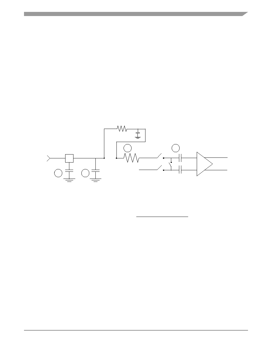
Equivalent Circuit for ADC Inputs
56F8013 Technical Data, Rev. 2
Freescale Semiconductor
111
Preliminary
10.15 Equivalent Circuit for ADC Inputs
Figure 10-17
illustrates the ADC input circuit during sample and hold. S1 and S2 are always open/closed
at the same time that S3 is closed/open. When S1/S2 are closed & S3 is open, one input of the sample and
hold circuit moves to (V
REFH
-V
REFL
)/2, while the other charges to the analog input voltage. When the
switches are flipped, the charge on C1 and C2 are averaged via S3, with the result that a single-ended
analog input is switched to a differential voltage centered about (V
REFH
-V
REFL
)/2. The switches switch
on every cycle of the ADC clock (open one-half ADC clock, closed one-half ADC clock). Note that there
are additional capacitances associated with the analog input pad, routing, etc., but these do not filter into
the S/H output voltage, as S1 provides isolation during the charge-sharing phase.
One aspect of this circuit is that there is an on-going input current, which is a function of the analog input
voltage, V
REF
and the ADC clock frequency.
1.
Parasitic capacitance due to package, pin-to-pin and pin-to-package base coupling; 1.8pF
2.
Parasitic capacitance due to the chip bond pad, ESD protection devices and signal routing; 2.04pF
3.
Equivalent resistance for the channel select mux; 100 ohms
4.
Sampling capacitor at the sample and hold circuit. Capacitor C1 is normally disconnected from the input and is only
connected to it at sampling time; 1.4pF
5.
Equivalent input impedance, when the the input is selected =
Figure 10-17 Equivalent Circuit for A/D Loading
1
2
3
Analog Input
4
S1
S2
S3
C1
C2
S/H
C1 = C2 = 1pF
(V
REFH
- V
REFL )
/ 2
125
ESD Resistor
8pF noise damping capacitor
1
(ADC Clock Rate) x 1.4 x 10
-12

56F8013 Technical Data, Rev. 2
112
Freescale Semiconductor
Preliminary
10.16 Power Consumption
See
Section 10.1
for a list of IDD requirements for the 56F8013. This section provides additional detail
which can be used to optimize power consumption for a given application.
Power consumption is given by the following equation:
A, the internal [static component], is comprised of the DC bias currents for the oscillator, leakage currents,
PLL, and voltage references. These sources operate independently of processor state or operating
frequency.
B, the internal [state-dependent component], reflects the supply current required by certain on-chip
resources only when those resources are in use. These include RAM, Flash memory and the ADCs.
C, the internal [dynamic component], is classic C*V
2
*F CMOS power dissipation corresponding to the
56800E core and standard cell logic.
D, the external [dynamic component], reflects power dissipated on-chip as a result of capacitive loading
on the external pins of the chip. This is also commonly described as C*V
2
*F, although simulations on two
of the I/O cell types used on the 56800E reveal that the power-versus-load curve does have a non-zero
Y-intercept.
Power due to capacitive loading on output pins is (first order) a function of the capacitive load and
frequency at which the outputs change.
Table 10-20
provides coefficients for calculating power dissipated
in the I/O cells as a function of capacitive load. In these cases:
TotalPower =
((Intercept + Slope*Cload)*frequency/10MHz)
Total power =
A: internal [static component]
+B: internal [state-dependent component]
+C: internal [dynamic component]
+D: external [dynamic component]
+E: external [static]
Table 10-20 I/O Loading Coefficients at 10MHz
Intercept
Slope
8mA drive
1.3
0.11mW / pF
4mA drive
1.15mW
0.11mW / pF

Power Consumption
56F8013 Technical Data, Rev. 2
Freescale Semiconductor
113
Preliminary
where:
∑
Summation is performed over all output pins with capacitive loads
∑
TotalPower is expressed in mW
∑
Cload is expressed in pF
Because of the low duty cycle on most device pins, power dissipation due to capacitive loads was found
to be fairly low when averaged over a period of time.
E, the external [static component], reflects the effects of placing resistive loads on the outputs of the
device. Sum the total of all V
2
/R or IV to arrive at the resistive load contribution to power. Assume V = 0.5
for the purposes of these rough calculations. For instance, if there is a total of eight PWM outputs driving
10mA into LEDs, then P = 8*.5*.01 = 40mW.
In previous discussions, power consumption due to parasitics associated with pure input pins is ignored,
as it is assumed to be negligible.
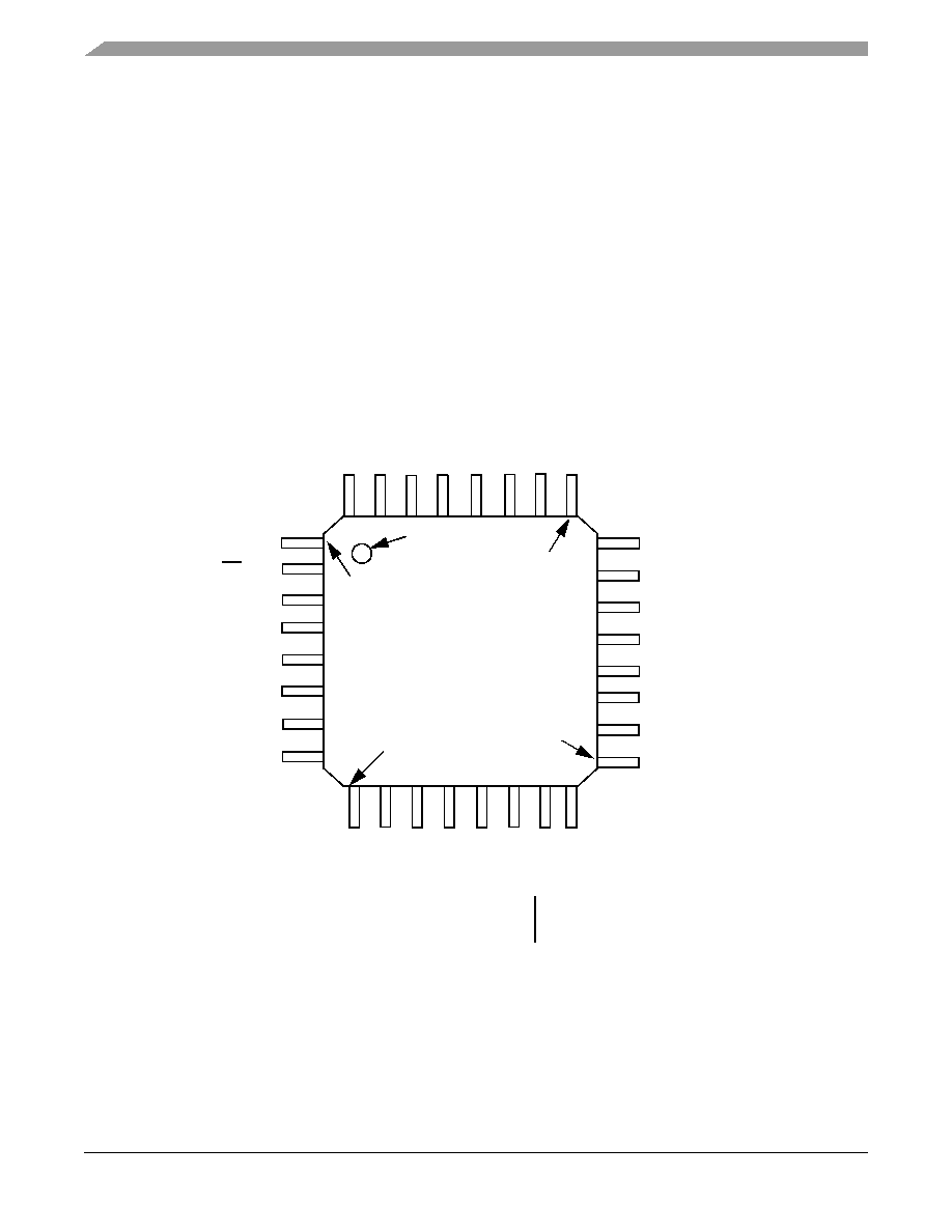
56F8013 Technical Data, Rev. 2
114
Freescale Semiconductor
Preliminary
Part 11 Packaging
11.1 56F8013 Package and Pin-Out Information
This section contains package and pin-out information for the 56F8013. This device comes in a 32-pin
Low-profile Quad Flat Pack (LQFP).
Figure 11-1
shows the package outline for the 32-pin LQFP,
Figure 11-2
shows the mechanical parameters for this package, and
Table 11-1
lists the pin-out for the
32-pin LQFP.
Figure 11-1 Top View, 56F8013 32-Pin LQFP Package
PIN 1
ORIENTATION
MARK
PIN 25
PIN 1
7
56F8013
PIN 9
GPIOB6/RXD/SDA/CLKIN
GPIOB1/SS/SDA
GPIOB7/TXD/SCL
GPIOB5/T1/FAULT3
ANB0/GPIOC4
ANB1/GPIOC5
ANB2/V
REFL
/GPIOC6
V
DDA
GPIOB2/MISO/T2
GPIOA6/FAULT0
GPIOB4/T0/CLKO
GPIOA5/PWM5/FAULT2/T3
GPIOB0/SCLK/SCL
GPIOA4/PWM4/FAULT1/T2
GPIOA2/PWM2
GPIOA3/PWM3
GPI
O
A1
/
PWM
1
V
CAP
V
SS_
I
O
V
DD_
I
O
GPI
O
A0
/
PWM
0
TDI
/
GP
I
O
D
0
TM
S
/
GPI
O
D3
TDO
/
GPI
O
D1
V
SSA
ANA
2
/
V
RE
F
H
/
GPI
O
C2
ANA1
/
GPI
O
C1
ANA0
/
GPI
O
C0
V
SS_
I
O
TCK
/
GPI
O
D2
RESET
/
GPI
O
A7
GP
I
O
B
3
/
MO
S
I
/
T
3
Note: Alternate signals are in iltalic

56F8013 Package and Pin-Out Information
56F8013 Technical Data, Rev. 2
Freescale Semiconductor
115
Preliminary
Table 11-1 56F8013 32-Pin LQFP Package Identification by Pin Number
1
1.Alternate signals are in iltalic
Pin
No.
Signal Name
Pin
No.
Signal Name
Pin
No.
Signal Name
Pin
No.
Signal Name
1
GPIOB6
RXD,SDA,CLKIN
9
V
SSA
17
GPIOB2
MISO,T2
25
V
CAP
2
GPIOB1
SS,SDA
10
ANA2
V
REFH
,GPIOC2
18
GPIOA6
FAULT0
26
V
DD_IO
3
GPIOB7
TXD,SCL
11
ANA1
GPIOC1
19
GPIOB4
T0,CLKO
27
V
SS_IO
4
GPIOB5
T1,FAULT3
12
ANA0
GPIOC0
20
GPIOA5
PWM5,FAULT2,T3
28
GPIOA1
PWM1
5
ANB0
GPIOC4
13
V
SS_IO
21
GPIOB0
SCLK,SCL
28
GPIOA0
PWM0
6
ANB1
GPIOC5
14
TCK
GPIOD2
22
GPIOA4
PWM4,FAULT1,T2
30
TDI
GPIOD0
7
ANB2
V
REFL
,GPIOC6
15
RESET
GPIOA7
23
GPIOA2
PWM2
31
TMS
GPIOD3
8
V
DDA
16
GPIOB3
MOSI,T3
24
GPIOA3
PWM3
32
TDO
GPIOD1
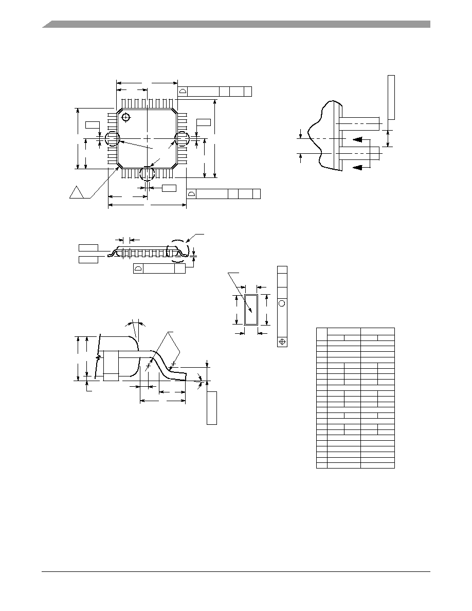
56F8013 Technical Data, Rev. 2
116
Freescale Semiconductor
Preliminary
Figure 11-2 56F8013 32-Pin LQFP Mechanical Information
……
……
……
……
DETAIL Y
A
S1
V
B
1
8
9
17
25
32
AE
AE
P
DETAIL Y
BASE
N
J
D
F
METAL
SECTION AE≠AE
G
SEATING
PLANE
R
Q
_
W
K
X
0.250 (0.010)
GAUGE PLANE
E
C
H
DETAIL AD
NOTES:
1. DIMENSIONING AND TOLERANCING PER ANSI
Y14.5M, 1982.
2. CONTROLLING DIMENSION: MILLIMETER.
3. DATUM PLANE ≠AB≠ IS LOCATED AT BOTTOM
OF LEAD AND IS COINCIDENT WITH THE LEAD
WHERE THE LEAD EXITS THE PLASTIC BODY AT
THE BOTTOM OF THE PARTING LINE.
4. DATUMS ≠T≠, ≠U≠, AND ≠Z≠ TO BE DETERMINED
AT DATUM PLANE ≠AB≠.
5. DIMENSIONS S AND V TO BE DETERMINED AT
SEATING PLANE ≠AC≠.
6. DIMENSIONS A AND B DO NOT INCLUDE MOLD
PROTRUSION. ALLOWABLE PROTRUSION IS
0.250 (0.010) PER SIDE. DIMENSIONS A AND B
DO INCLUDE MOLD MISMATCH AND ARE
DETERMINED AT DATUM PLANE ≠AB≠.
7. DIMENSION D DOES NOT INCLUDE DAMBAR
PROTRUSION. DAMBAR PROTRUSION SHALL
NOT CAUSE THE D DIMENSION TO EXCEED
0.520 (0.020).
8. MINIMUM SOLDER PLATE THICKNESS SHALL BE
0.0076 (0.0003).
9. EXACT SHAPE OF EACH CORNER MAY VARY
FROM DEPICTION.
DIM
A
MIN
MAX
MIN
MAX
INCHES
7.000 BSC
0.276 BSC
MILLIMETERS
B
7.000 BSC
0.276 BSC
C
1.400
1.600
0.055
0.063
D
0.300
0.450
0.012
0.018
E
1.350
1.450
0.053
0.057
F
0.300
0.400
0.012
0.016
G
0.800 BSC
0.031 BSC
H
0.050
0.150
0.002
0.006
J
0.090
0.200
0.004
0.008
K
0.500
0.700
0.020
0.028
M
12 REF
12 REF
N
0.090
0.160
0.004
0.006
P
0.400 BSC
0.016 BSC
Q
1
5
1
5
R
0.150
0.250
0.006
0.010
V
9.000 BSC
0.354 BSC
V1
4.500 BSC
0.177 BSC
_
_
_
_
_
_
DETAIL AD
A1
B1
V1
4X
S
4X
B1
3.500 BSC
0.138 BSC
A1
3.500 BSC
0.138 BSC
S
9.000 BSC
0.354 BSC
S1
4.500 BSC
0.177 BSC
W
0.200 REF
0.008 REF
X
1.000 REF
0.039 REF
9
≠T≠
≠Z≠
≠U≠
T≠U
0.20 (0.008)
Z
AC
T≠U
0.20 (0.008)
Z
AB
0.10 (0.004) AC
≠AC≠
≠AB≠
M
_
8X
≠T≠, ≠U≠, ≠Z≠
T≠U
M
0.20 (0.008)
Z
AC

Thermal Design Considerations
56F8013 Technical Data, Rev. 2
Freescale Semiconductor
117
Preliminary
Part 12 Design Considerations
12.1 Thermal Design Considerations
An estimation of the chip junction temperature, T
J
, can be obtained from the equation:
T
J
= T
A
+ (R
J
x
P
D
)
where:
The junction-to-ambient thermal resistance is an industry-standard value that provides a quick and easy
estimation of thermal performance. Unfortunately, there are two values in common usage: the value
determined on a single-layer board and the value obtained on a board with two planes. For packages such
as the PBGA, these values can be different by a factor of two. Which value is closer to the application
depends on the power dissipated by other components on the board. The value obtained on a single layer
board is appropriate for the tightly packed printed circuit board. The value obtained on the board with the
internal planes is usually appropriate if the board has low-power dissipation and the components are well
separated.
When a heat sink is used, the thermal resistance is expressed as the sum of a junction-to-case thermal
resistance and a case-to-ambient thermal resistance:
R
JA
= R
JC
+ R
CA
where:
R
JC
is device related and cannot be influenced by the user. The user controls the thermal environment to
change the case to ambient thermal resistance, R
CA
. For instance, the user can change the size of the heat
sink, the air flow around the device, the interface material, the mounting arrangement on printed circuit
board, or change the thermal dissipation on the printed circuit board surrounding the device.
To determine the junction temperature of the device in the application when heat sinks are not used, the
Thermal Characterization Parameter (
JT
) can be used to determine the junction temperature with a
measurement of the temperature at the top center of the package case using the following equation:
T
J
= T
T
+ (
JT
x P
D
)
where:
T
A
= Ambient temperature for the package (
o
C)
R
J
= Junction-to-ambient thermal resistance (
o
C/W)
P
D
= Power dissipation in the package (W)
R
JA
= Package junction-to-ambient thermal resistance (∞C/W)
R
JC
= Package junction-to-case thermal resistance (∞C/W)
R
CA
= Package case-to-ambient thermal resistance (∞C/W)
T
T
= Thermocouple temperature on top of package (
o
C)
JT
= Thermal characterization parameter (
o
C/W)
P
D
= Power dissipation in package (W)

56F8013 Technical Data, Rev. 2
118
Freescale Semiconductor
Preliminary
The thermal characterization parameter is measured per JESD51-2 specification using a 40-gauge type T
thermocouple epoxied to the top center of the package case. The thermocouple should be positioned so
that the thermocouple junction rests on the package. A small amount of epoxy is placed over the
thermocouple junction and over about 1mm of wire extending from the junction. The thermocouple wire
is placed flat against the package case to avoid measurement errors caused by cooling effects of the
thermocouple wire.
When heat sink is used, the junction temperature is determined from a thermocouple inserted at the
interface between the case of the package and the interface material. A clearance slot or hole is normally
required in the heat sink. Minimizing the size of the clearance is important to minimize the change in
thermal performance caused by removing part of the thermal interface to the heat sink. Because of the
experimental difficulties with this technique, many engineers measure the heat sink temperature and then
back-calculate the case temperature using a separate measurement of the thermal resistance of the
interface. From this case temperature, the junction temperature is determined from the junction-to-case
thermal resistance.
12.2 Electrical Design Considerations
Use the following list of considerations to assure correct operation of the 56F8013:
∑
Provide a low-impedance path from the board power supply to each V
DD
pin on the 56F8013 and from the
board ground to each V
SS
(GND) pin
∑
The minimum bypass requirement is to place 0.01≠0.1
µF capacitors positioned as close as possible to the
package supply pins. The recommended bypass configuration is to place one bypass capacitor on each of
the V
DD
/V
SS
pairs, including V
DDA
/V
SSA.
Ceramic and tantalum capacitors tend to provide better
tolerances.
∑
Ensure that capacitor leads and associated printed circuit traces that connect to the chip V
DD
and V
SS
(GND)
pins are as short as possible
∑
Bypass the V
DD
and V
SS
with approximately 100
µF, plus the number of 0.1µF ceramic capacitors
∑
PCB trace lengths should be minimal for high-frequency signals
∑
Consider all device loads as well as parasitic capacitance due to PCB traces when calculating capacitance.
This is especially critical in systems with higher capacitive loads that could create higher transient currents
in the V
DD
and V
SS
circuits.
CAUTION
This device contains protective circuitry to guard
against damage due to high static voltage or electrical
fields. However, normal precautions are advised to
avoid application of any voltages higher than
maximum-rated voltages to this high-impedance circuit.
Reliability of operation is enhanced if unused inputs are
tied to an appropriate voltage level.

Electrical Design Considerations
56F8013 Technical Data, Rev. 2
Freescale Semiconductor
119
Preliminary
∑
Take special care to minimize noise levels on the V
REF
, V
DDA
and V
SSA
pins
∑
Using separate power planes for V
DD
and V
DDA
and separate ground planes for V
SS
and V
SSA
is
recommended. Connect the separate analog and digital power and ground planes as close as possible to
power supply outputs. If both analog circuit and digital circuit are powered by the same power supply, it is
advisable to connect a small inductor or ferrite bead in serial with both V
DDA
and V
SSA
traces.
∑
It is highly desirable to physically separate analog components from noisy digital components by ground
planes. Do not place an analog trace in parallel with digital traces. It is also desirable to place an analog
ground trace around an analog signal trace to isolate it from digital traces.
∑
Because the Flash memory is programmed through the JTAG/EOnCE port, SPI, SCI or I
2
C, the designer
should provide an interface to this port if in-circuit Flash programming is desired.
Part 13 Ordering Information
Table 13-1
lists the pertinent information needed to place an order. Consult a Freescale Semiconductor
sales office or authorized distributor to determine availability and to order parts.
Table 13-1 56F8013 Ordering Information
Part
Supply
Voltage
Package Type
Pin
Count
Frequency
(MHz)
Temperature
Range
Order Number
MC56F8013
3.0≠3.6 V
Low-Profile Quad Flat Pack (LQFP)
32
32
-40∞ to + 105∞ C
MC56F8013VFAE

56F8013 Technical Data, Rev. 2
120
Freescale Semiconductor
Preliminary
Part 14 Appendix
Register acronyms are revised from previous device data sheets to provide a cleaner register description.
A cross reference to legacy and revised acronyms are provided in the following table.
Module
Register Name
Peripheral Reference
Manual
Data Sheet
Processor
Expert
Acronym
Memory
Address
New
Acronym
Legacy
Acronym
New Acronym Legacy Acronym
Start
End
ADC
Control Register 1
CTRL1
ADCR1
ADC_CTRL1
ADC_ADCR1
ADC_ADCR1
0xF080
Control Register 2
CTRL2
ADCR2
ADC_CTRL2
ADC_ADCR2
ADC_ADCR2
0xF081
Zero Crossing Control Register
ZXCTRL
ADZCC
ADC_ZXCTRL
ADC_ADZCC
ADC_ADZCC
0xF082
Channel List Register 1
CLIST1
ADLST1
ADC_CLIST1
ADC_ADLST1
ADC_ADLST1
0xF083
Channel List Register 2
CLIST2
ADLST2
ADC_CLIST2
ADC_ADLST2
ADC_ADLST2
0xF084
Sample Disable Register
SDIS
ADSDIS
ADC_SDIS
ADC_ADSDIS
ADC_ADSDIS
0xF085
Status Register
STAT
ADSTAT
ADC_STAT
ADC_ADSTAT
ADC_ADSTAT
0xF086
Limit Status Register
LIMSTAT
ADLSTAT
ADC_LIMSTAT
ADC_ADLSTAT
ADC_ADLSTAT
0xF087
Zero Crossing Status Register
ZXSTAT
ADZCSTAT
ADC_ZXSTAT ADC_ADZCSTAT ADC_ADZCSTAT
0xF088
Result Registers 0-7
RSLT0-7
ADRSLT0-7
ADC_RSLT0-7 ADC_ADRSLT0-7 ADC_ADRSLT0-7 0xF089 0XF090
Low Limit Registers 0-7
LOLIM0-7
ADLLMT0-7
ADC_LOLIM0-7 ADC_ADLLMT0-7 ADC_ADLLMT0-7 0XF091 0XF098
High Limit Registers 0-7
HILIM0-7
ADHLMT0-7
ADC_HILIM0-7 ADC_ADHLMT0-7 ADC_ADHLMT0-7 0XF099 0XF0A0
Offset Registers 0-7
OFFST0-7
ADOFS0-7
ADC_OFFST0-7 ADC_ADOFS0-7
ADC_ADOFS0-7 0XF0A1 0XF0A8
Power Control Register
PWR
ADPOWER
ADC_PWR
ADC_ADPOWER ADC_ADPOWER
0XF0A9
Voltage Reference Register
CAL
ADCAL
ADC_VREF
ADC_ADCAL
ADC_CAL
0XF0AA
COP
Control Register
CTRL
COPCTL
COP_CTRL
COPCTL
COPCTL
0XF0E0
Time-Out Register
TOUT
COPTO
COP_TOUT
COPTO
COPTO
0XF0E1
Counter Register
CNTR
COPCTR
COP_CNTR
COPCTR
COPCTR
0XF0E2
I
2
C
Address Register
ADDR
IBAD
I2C_ADDR
I2C_IBAD
IBAD
0xF0D0
Frequency Divider Register
FDIV
IBFD
I2C_FDIV
I2C_IBFD
IBFD
0xF0D1
Control Register
CTRL
IBCR
I2C_CTRL
I2C_IBCR
IBCR
0xF0D2
Status Register
STAT
IBSR
I2C_STAT
I2C_IBSR
IBSR
0xF0D3
Data I./O Register
DATA
IBDR
I2C_DATA
I2C_IBDR
IBDR
0xF0D4
Noise Filter Register
NFILT
IBNR
I2C_NFILT
I2C_IBNR
IBNR
0xF0D5
ITCN Interrupt Priority Register 0-4
N/A
N/A
ITCN_IPR0-4
ITCN_IPR0-4
INTC_IPR0-4
0XF060 0XF064
Vector Base Address Register
N/A
N/A
ITCN_VBA
ITCN_VBA
INTC_VBA
0XF065
Fast Interrupt Match 0 Register
N/A
N/A
ITCN_FIM0
ITCN_FIM0
INTC_FIM0
0XF066
Fast Interrupt Vector Address Low 0
N/A
N/A
ITCN_FIVAL0
ITCN_FIVAL0
INTC_FIVAL0
0XF067
Fast Interrupt Vector Address High 0
N/A
N/A
ITCN_FIVAH0
ITCN_FIVAH0
INTC_FIVAH0
0XF068
Fast Interrupt Match 1 Register
N/A
N/A
ITCN_FIM1
ITCN_FIM1
INTC_FIM1
0xF069
Fast Interrupt Vector Address Low 1
N/A
N/A
ITCN_FIVAL1
ITCN_FIVAL1
INTC_FIVAL1
0xF06A
Fast Interrupt Vector Address High 1
N/A
N/A
ITCN_FIVAH1
ITCN_FIVAH1
INTC_FIVAH1
0xF06B
Interrupt Pending Register 0
N/A
N/A
ITCN_IRQP0
ITCN_IRQP0
INTC_IRQP0
0xF06C
Interrupt Pending Register 1
N/A
N/A
ITCN_IRQP1
ITCN_IRQP1
INTC_IRQP1
0xF06D
Interrupt Pending Register 2
N/A
N/A
ITCN_IRQP2
ITCN_IRQP2
INTC_IRQP2
0xF06E
Interrupt Control Register
N/A
N/A
ITCN_ICTRL
ITCN_ICTL
INTC_ICTL
0xF072
Electrical Design Considerations
56F8013 Technical Data, Rev. 2
Freescale Semiconductor
121
Preliminary
Module
Register Name
Peripheral Reference
Manual
Data Sheet
Processor
Expert
Acronym
Memory
Address
New
Acronym
Legacy
Acronym
New Acronym Legacy Acronym
Start
End
OCCS Control Register
CTRL
PLLCR
OCCS_CTRL
PLLCR
PLLCR
0xF0F0
Divide-By Register
DIVBY
PLLDB
OCCS_DIVBY
PLLDB
PLLDB
0xF0F1
Status Register
STAT
PLLSR
OCCS_STAT
PLLSR
PLLSR
0xF0F2
Shutdown Register
SHUTDN
SHUTDOWN OCCS_SHUTDN
SHUTDOWN
SHUTDOWN
0xF0F4
Oscillator Control Register
OCTRL
OSCTL
OCCS_OCTRL
OSCTL
OSCTL
0xF0F5
FM
Clock Divider Register
CLKDIV
FMCLKD
FM_CLKDIV
FMCLKD
FMCLKD
0xF400
Configuration Register
CNFG
FMCR
FM_CNFG
FMCR
FMCR
0xF401
Security High Half Register
SECHI
FMSECH
FM_SECHI
FMSECH
FMSECH
0xF403
Security Low Half Register
SECLO
FMSECL
FM_SECLO
FMSECL
FMSECL
0xF404
Protection Register
PROT
FMPROT
FM_PROT
FMPROT
FMPROT
0xF410
User Status Register
USTAT
FMUSTAT
FM_USTAT
FMUSTAT
FMUSTAT
0xF413
Command Register
CMD
FMCMD
FM_CMD
FMCMD
FMCMD
0xF414
Address Register
ADDR
FMADDR
FM_ADDR
FMADDR
0xF416
Data Buffer Register
DATA
FMDATA
FM_DATA
FMDATA
0xF418
Optional Data 1 Register
OPT1
FMOPT1
FM_OPT1
FMOPT1
FMOPT1
0xF41B
Test Array Signature Register
TSTSIG
FMTST_SIG
FM_TSTSIG
FMTST_SIG
0xF41D
x = A (n=0) B (n=1) C (n=2) D (n=3)
GPIO Pull-Up Enable Register
PUPEN
PUR
GPIOx_PUPEN
GPIOx_PUR
GPIO_x_PUR
0xF1n0
Data Register
DATA
DR
GPIOx_DATA
GPIOx_DR
GPIO_x_DR
0xF1n1
Data Direction Register
DDIR
DDR
GPIOx_DDIR
GPIOx_DDR
GPIO_x_DDR
0xF1n2
Peripheral Enable Register
PEREN
PER
GPIOx_PEREN
GPIOx_PER
GPIO_x_PER
0xF1n3
Interrupt Assert Register
IASSRT
IAR
GPIOx_IASSRT
GPIOx_IAR
GPIO_x_IAR
0xF1n4
Interrupt Enable Register
IEN
IENR
GPIOx_IEN
GPIOx_IENR
GPIO_x_IENR
0xF1n5
Interrupt Edge Polarity Register
IEPOL
IPOLR
GPIOx_IEPOL
GPIOx_IPOLR
GPIO_x_IPOLR
0xF1n6
Interrupt Pending Register
IPEND
IPR
GPIOx_IPEND
GPIOx_IPR
GPIO_x_IPR
0xF1n7
Interrupt Edge Sensitive Register
IEDGE
IESR
GPIOx_IEDGE
GPIOx_IESR
GPIO_x_IESR
0xF1n8
Push-Pull Output Mode Control Register
PPOUTM
PPMODE
GPIOx_PPOUTM
GPIOx_PPMODE GPIO_x_PPMODE
0xF1n9
Raw Data Register
RDATA
RAWDATA
GPIOx_RDATA GPIOx_RAWDATA GPIO_x_RAWDATA
0xF1nA
Drive Strength Control Register
DRIVE
DRIVE
GPIOx_DRIVE
GPIOx_DRIVE
GPIO_x_DRIVE
0xF1nB
PS
Control Register
CTRL
LVICONTROL
PS_CTRL
LVICONTROL
LVICTRL
0xF160
Status Register
STAT
LVISTATUS
PS_STAT
LVISTATUS
LVISR
0xF161
56F8013 Technical Data, Rev. 2
122
Freescale Semiconductor
Preliminary
Module
Register Name
Peripheral Reference
Manual
Data Sheet
Processor
Expert
Acronym
Memory
Address
New
Acronym
Legacy
Acronym
New Acronym Legacy Acronym
Start
End
PWM Control Register
CTRL
PMCTL
PWM_CTRL
PWM_PMCTL
PWM_PMCTL
0xF040
Fault Control Register
FCTRL
PMFCTL
PWM_FCTRL
PWM_PMFCTL
PWM_PMFCTL
0xF041
Fault Status/Acknowledge Regis.
FLTACK
PMFSA
PWM_FLTACK
PWM_PMFSA
PWM_PMFSA
0xF042
Output Control Register
OUT
PMOUT
PWM_OUT
PWM_PMOUT
PWM_PMOUT
0xF043
Counter Register
CNTR
PMCNT
PWM_CNTR
PWM_PMCNT
PWM_PMCNT
0xF044
Counter Modulo Register
CMOD
MCM
PWM_CMOD
PWM_MCM
PWM_PWMCM
0xF045
Value Register 0-5
VAL0-5
PMVAL0-5
PWM_VAL0-5
PWM_PMVAL0-5 PWM_PWMVAL0-5 0xF046 0xF04B
Deadtime Register 0-1
DTIM0-1
PMDEADTM0-1
PWM_DTIM0-1
PWM_PMDEADTM0-1 PWM_PMDEADTM0-1
0xF04C 0xF04D
Disable Mapping Register 1-2
DMAP1-2
PMDISMAP1-2 PWM_DMAP1-2
PWM_PMDISMAP1-2
PWM_PMDISMAP1-2
0xF04E 0xF04F
Configure Register
CNFG
PMCFG
PWM_CNFG
PWM_PMCFG
PWM_PMCFG
0xF050
Channel Control Register
CCTRL
PMCCR
PWM_CCTRL
PWM_PMCCR
PWM_PMCCR
0xF051
Port Register
PORT
PMPORT
PWM_PORT
PWM_PMPORT
PWM_PMPORT
0xF052
Internal Correction Control Regis.
ICCTRL
PMICCR
PWM_ICCTRL
PWM_PMICCR
PWM_PMICCR
0xF053
Source Control Register
SCTRL
PMSRC
PWM_SCTRL
PWM_PMSRC
PWM_PMSRC
0xF054
SCI
Baud Rate Register
RATE
SCIBR
SCI_RATE
SCI_SCIBR
SCI_SCIBR
0xF0B0
Control Register 1
CTRL1
SCICR
SCI_CTRL1
SCI_SCICR
SCI_SCICR
0xF0B1
Control Register 2
CTRL2
SCICR2
SCI_CTRL2
SCI_SCICR2
SCI_SCICR2
0xF0B2
Status Register
STAT
SCISR
SCI_STAT
SCI_SCISR
SCI_SCISR
0xF0B3
Data Register
DATA
SCIDR
SCI_DATA
SCI_SCIDR
SCI_SCIDR
0xF0B4
SIM
Control Register
N/A
N/A
SIM_CTRL
SIM_CONTROL
SIM_CONTROL
0xF140
Reset Status Register
N/A
N/A
SIM_RSTAT
SIM_RSTSTS
SIM_RSTSTS
0xF141
Software Control Register 0-3
N/A
N/A
SIM_SWC0-3
SIM_SCR0-3
SIM_SCR0-3
0xF142 0xF145
Most Significant Half JTAG ID
N/A
N/A
SIM_MSHID
SIM_MSH_ID
SIM_MSH_ID
0xF146
Least Significant Half JTAG ID
N/A
N/A
SIM_LSHID
SIM_LSH_ID
SIM_LSH_ID
0xF147
Power Control Register
N/A
N/A
SIM_PWR
SIM_POWER
0xF148
Clock Out Select Register
N/A
N/A
SIM_CLKOUT
SIM_CLKOSR
SIM_CLKOSR
0xF14A
GPIO Peripheral Select Register
N/A
N/A
SIM_GPS
SIM_GPS
SIM_GPS
0xF14B
Peripheral Clock Enable Register
N/A
N/A
SIM_PCE
SIM_PCE
SIM_PCE
0xF14C
I/O Short Address Location High
N/A
N/A
SIM_IOSAHI
SIM_ISALH
SIM_ISALH
0xF14D
I/O Short Address Location Low
N/A
N/A
SIM_IOSALO
SIM_ISALL
SIM_ISALL
0xF14E
SPI
Status and Control Register
SCTRL
SPSCR
SPI_SCTRL
SPI_SPSCR
SPI_SCR
0xF0C0
Data Size and Control Register
DSCTRL
SPDSR
SPI_DSCTRL
SPI_SPDSR
SPI_DSR
0xF0C1
Data Receive Register
DRCV
SPDRR
SPI_DRCV
SPI_SPDRR
SPI_DRR
0xF0C2
Data Transmit Register
DXMIT
SPDTR
SPI_DXMIT
SPI_SPDTR
SPI_DTR
0xF0C3
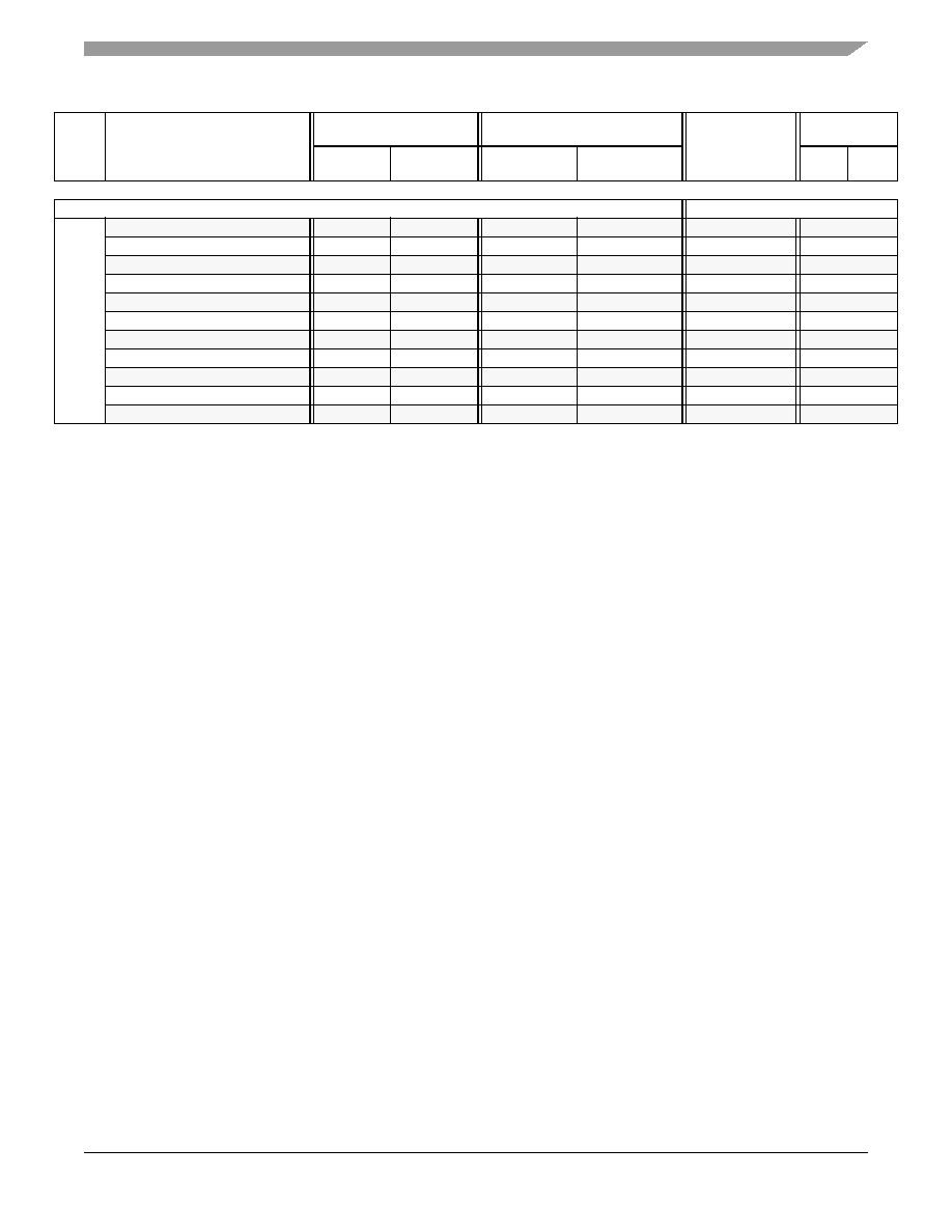
Electrical Design Considerations
56F8013 Technical Data, Rev. 2
Freescale Semiconductor
123
Preliminary
Module
Register Name
Peripheral Reference
Manual
Data Sheet
Processor
Expert
Acronym
Memory
Address
New
Acronym
Legacy
Acronym
New Acronym Legacy Acronym
Start
End
n = 0, 1, 2, 3
TMR
Compare Register 1
COMP1
TMRCMP1
TMRn_COMP1
TMRn_CMP1
TMRn_CMP1
0xF0n0
Compare Register 2
COMP2
TMRCMP2
TMRn_COMP2
TMRn_CMP2
TMRn_CMP2
0xF0n1
Capture Register
CAPT
TMRCAP
TMRn_CAPT
TMRn_CAP
TMRn_CAP
0xF0n2
Load Register
LOAD
TMRLOAD
TMRn_LOAD
TMRn_LOAD
TMRn_LOAD
0xF0n3
Hold Register
HOLD
TMRHOLD
TMRn_HOLD
TMRn_HOLD
TMRn_HOLD
0xF0n4
Counter Register
CNTR
TMRCNTR
TMRn_CNTR
TMRn_CNTR
TMRn_CNTR
0xF0n5
Control Register
CTRL
TMRCTRL
TMRn_CTRL
TMRn_CTRL
TMRn_CTRL
0xF0n6
Status and Control Register
SCTRL
TMRSCR
TMRn_SCTRL
TMRn_SCR
TMRn_SCR
0xF0n7
Comparator Load Register 1
CMPLD1
TMRCMPLD1 TMRn_CMPLD1 TMRn_CMPLD1
TMRn_CMPLD1
0xF0n8
Comparator Load Register 2
CMPLD2
TMRCMPLD2 TMRn_CMPLD2 TMRn_CMPLD2
TMRn_CMPLD2
0xF0n9
Comparator Status/Control Register
CSCTRL
TMRCOMSCR TMRn_CSCTRL TMRn_COMSCR
TMRn_COMSCR
0xF0nA

How to Reach Us:
Home Page:
www.freescale.com
E-mail:
support@freescale.com
USA/Europe or Locations Not Listed:
Freescale Semiconductor
Technical Information Center, CH370
1300 N. Alma School Road
Chandler, Arizona 85224
+1-800-521-6274 or +1-480-768-2130
support@freescale.com
Europe, Middle East, and Africa:
Freescale Halbleiter Deutschland GmbH
Technical Information Center
Schatzbogen 7
81829 Muenchen, Germany
+44 1296 380 456 (English)
+46 8 52200080 (English)
+49 89 92103 559 (German)
+33 1 69 35 48 48 (French)
support@freescale.com
Japan:
Freescale Semiconductor Japan Ltd.
Headquarters
ARCO Tower 15F
1-8-1, Shimo-Meguro, Meguro-ku,
Tokyo 153-0064, Japan
0120 191014 or +81 3 5437 9125
support.japan@freescale.com
Asia/Pacific:
Freescale Semiconductor Hong Kong Ltd.
Technical Information Center
2 Dai King Street
Tai Po Industrial Estate
Tai Po, N.T., Hong Kong
+800 2666 8080
support.asia@freescale.com
For Literature Requests Only:
Freescale Semiconductor Literature Distribution Center
P.O. Box 5405
Denver, Colorado 80217
1-800-441-2447 or 303-675-2140
Fax: 303-675-2150
LDCForFreescaleSemiconductor@hibbertgroup.com
FreescaleTM and the Freescale logo are trademarks of Freescale Semiconductor,
Inc. All other product or service names are the property of their respective owners.
This product incorporates SuperFlashÆ technology licensed from SST.
© Freescale Semiconductor, Inc. 2005. All rights reserved.
MC56F8013
Rev. 2
4/2005
Information in this document is provided solely to enable system and
software implementers to use Freescale Semiconductor products. There are
no express or implied copyright licenses granted hereunder to design or
fabricate any integrated circuits or integrated circuits based on the
information in this document.
Freescale Semiconductor reserves the right to make changes without further
notice to any products herein. Freescale Semiconductor makes no warranty,
representation or guarantee regarding the suitability of its products for any
particular purpose, nor does Freescale Semiconductor assume any liability
arising out of the application or use of any product or circuit, and specifically
disclaims any and all liability, including without limitation consequential or
incidental damages. "Typical" parameters that may be provided in Freescale
Semiconductor data sheets and/or specifications can and do vary in different
applications and actual performance may vary over time. All operating
parameters, including "Typicals", must be validated for each customer
application by customer's technical experts. Freescale Semiconductor does
not convey any license under its patent rights nor the rights of others.
Freescale Semiconductor products are not designed, intended, or authorized
for use as components in systems intended for surgical implant into the body,
or other applications intended to support or sustain life, or for any other
application in which the failure of the Freescale Semiconductor product could
create a situation where personal injury or death may occur. Should Buyer
purchase or use Freescale Semiconductor products for any such unintended
or unauthorized application, Buyer shall indemnify and hold Freescale
Semiconductor and its officers, employees, subsidiaries, affiliates, and
distributors harmless against all claims, costs, damages, and expenses, and
reasonable attorney fees arising out of, directly or indirectly, any claim of
personal injury or death associated with such unintended or unauthorized
use, even if such claim alleges that Freescale Semiconductor was negligent
regarding the design or manufacture of the part.