
M68HC08M68H C08M68HC08M 68HC08M68HC
MC68HC
05PV8A
Technical Data
HCMOS
Microcontroller Unit
MC68HC05PV8/D
REV 1.9
F
r
e
e
s
c
a
l
e
S
e
m
i
c
o
n
d
u
c
t
o
r
,
I
Freescale Semiconductor, Inc.
For More Information On This Product,
Go to: www.freescale.com
n
c
.
.
.
MC68HC05PV8
MC68HC805PV8

F
r
e
e
s
c
a
l
e
S
e
m
i
c
o
n
d
u
c
t
o
r
,
I
Freescale Semiconductor, Inc.
For More Information On This Product,
Go to: www.freescale.com
n
c
.
.
.

MC68HC(8)05PV8/A -- Rev. 1.9
Technical Data
NO
NDI
S
CLO
S
URE AG
REEMENT
REQ
U
IRED
MC68HC05PV8
MC68HC805PV8
MC68HC05PV8A
Technical Data -- Rev 1.9
Motorola reserves the right to make changes without further notice to any products
herein. Motorola makes no warranty, representation or guarantee regarding the
suitability of its products for any particular purpose, nor does Motorola assume any
liability arising out of the application or use of any product or circuit, and specifically
disclaims any and all liability, including without limitation consequential or incidental
damages. "Typical" parameters which may be provided in Motorola data sheets and/or
specifications can and do vary in different applications and actual performance may
vary over time. All operating parameters, including "Typicals" must be validated for
each customer application by customer's technical experts. Motorola does not convey
any license under its patent rights nor the rights of others. Motorola products are not
designed, intended, or authorized for use as components in systems intended for
surgical implant into the body, or other applications intended to support or sustain life,
or for any other application in which the failure of the Motorola product could create a
situation where personal injury or death may occur. Should Buyer purchase or use
Motorola products for any such unintended or unauthorized application, Buyer shall
indemnify and hold Motorola and its officers, employees, subsidiaries, affiliates, and
distributors harmless against all claims, costs, damages, and expenses, and
reasonable attorney fees arising out of, directly or indirectly, any claim of personal
injury or death associated with such unintended or unauthorized use, even if such claim
alleges that Motorola was negligent regarding the design or manufacture of the part.
Motorola, Inc. is an Equal Opportunity/Affirmative Action Employer.
Motorola and
are registered trademarks of Motorola, Inc.
DigitalDNA is a trademark of Motorola, Inc.
� Motorola, Inc., 2001
Freescale
Semiconductor,
I
Freescale Semiconductor, Inc.
For More Information On This Product,
Go to: www.freescale.com
nc.
..

Technical Data
Technical Data
MC68HC(8)05PV8/A -- Rev. 1.9
NO
NDISCLOSURE AGREEMENT REQUIRED
Freescale
Semiconductor,
I
Freescale Semiconductor, Inc.
For More Information On This Product,
Go to: www.freescale.com
nc.
..

MC68HC(8)05PV8/A -- Rev. 1.9
Technical Data
Revision History
NO
NDI
S
CLO
S
URE AG
REEMENT
REQ
U
IRED
Technical Data -- MC68HC(8)05PV8/A
Revision History
Contents
Introduction
. . . . . . . . . . . . . . . . . . . . . . . . . . . . . . . . . . . . . . . . . . . . .
5
Changes from Rev 1.5 published on September 9th, 1999 to Rev 1.6
published on May 4th, 2000
. . . . . . . . . . . . . . . . . . . . . . . . . . . . . . . .
6
Changes from Rev 1.6 published on May 4th, 2000 to Rev 1.7 pub-
lished on December 1st, 2000
. . . . . . . . . . . . . . . . . . . . . . . . . . . . . .
6
Changes from Rev 1.7 published on December 1st, 2000 to Rev 1.8
published on February 20th, 2001
. . . . . . . . . . . . . . . . . . . . . . . . . . .
6
Changes from Rev 1.8 published on February 20th, 2001 to Rev 1.9
published on September 3th, 2001
. . . . . . . . . . . . . . . . . . . . . . . . . .
6
Introduction
This section contains the revision history for the MC68HC(8)05PV8/A
data book.
Freescale
Semiconductor,
I
Freescale Semiconductor, Inc.
For More Information On This Product,
Go to: www.freescale.com
nc.
..
Technical Data
Technical Data
MC68HC(8)05PV8/A -- Rev. 1.9
Revision History
NO
NDISCLOSURE AGREEMENT REQUIRED
Changes from Rev 1.5 published on September 9th, 1999 to Rev 1.6
published on May 4th, 2000
Changes from Rev 1.6 published on May 4th, 2000 to Rev 1.7 published on
December 1st, 2000
Changes from Rev 1.7 published on December 1st, 2000 to Rev 1.8
published on February 20th, 2001
Changes from Rev 1.8 published on February 20th, 2001 to Rev 1.9
published on September 3th, 2001
Section
Page (in Rev 1.6)
Description of change
added PV8A functionality, initial release
Section
Page (in Rev 1.7)
Description of change
2
33
added note 3
Section
Page (in Rev 1.8)
Description of change
16.15.1
185
removed PC4 input hysteresis for PV8A
16.15.1
185
added PC4 input debounce time for PV8A
Section
Page (in Rev 1.9)
Description of change
1.5
30
added mechanical specification
1.7
33
added ordering information
16.5
176
filled in typical value for I
SUP12
16.5
176
added I
SUP4A
16.12
185
added rise time specification on VDD
Freescale
Semiconductor,
I
Freescale Semiconductor, Inc.
For More Information On This Product,
Go to: www.freescale.com
nc.
..

List of Sections
MC68HC(8)05PV8/A -- Rev. 1.9
Technical Data
List of Sections
NO
NDI
S
CLO
S
URE AG
REEMENT
REQ
U
IRED
Revision History . . . . . . . . . . . . . . . . . . . . . . . . . . . . . . . . . 5
List of Sections . . . . . . . . . . . . . . . . . . . . . . . . . . . . . . . . . . 7
Table of Contents. . . . . . . . . . . . . . . . . . . . . . . . . . . . . . . . 9
List of Figures . . . . . . . . . . . . . . . . . . . . . . . . . . . . . . . . . . 19
List of Tables . . . . . . . . . . . . . . . . . . . . . . . . . . . . . . . . . . . 23
General Description . . . . . . . . . . . . . . . . . . . . . . . . . . . . 25
Memory . . . . . . . . . . . . . . . . . . . . . . . . . . . . . . . . . . . . . . 35
CPU and Instruction Set. . . . . . . . . . . . . . . . . . . . . . . . . . 43
Interrupts. . . . . . . . . . . . . . . . . . . . . . . . . . . . . . . . . . . . . . 65
Resets . . . . . . . . . . . . . . . . . . . . . . . . . . . . . . . . . . . . . . . . 77
Operating Modes . . . . . . . . . . . . . . . . . . . . . . . . . . . . . . 87
Input/Output Ports . . . . . . . . . . . . . . . . . . . . . . . . . . . . . . 93
Core Timer . . . . . . . . . . . . . . . . . . . . . . . . . . . . . . . . . . . 117
16-Bit Programmable Timer . . . . . . . . . . . . . . . . . . . . . 123
Analog to Digital Converter . . . . . . . . . . . . . . . . . . . . . 137
Pulse Width Modulator . . . . . . . . . . . . . . . . . . . . . . . . . 147
Voltage Regulator . . . . . . . . . . . . . . . . . . . . . . . . . . . . . 155
Technical Data -- MC68HC(8)05PV8/A
List of Sections
Freescale
Semiconductor,
I
Freescale Semiconductor, Inc.
For More Information On This Product,
Go to: www.freescale.com
nc.
..

Technical Data
Technical Data
MC68HC(8)05PV8/A -- Rev. 1.9
List of Sections
NO
NDISCLOSURE AGREEMENT REQUIRED
EEPROM. . . . . . . . . . . . . . . . . . . . . . . . . . . . . . . . . . . . . . 157
Program EEPROM . . . . . . . . . . . . . . . . . . . . . . . . . . . . . . 163
Fast Parallel Interface . . . . . . . . . . . . . . . . . . . . . . . . . . 169
Electrical Specifications . . . . . . . . . . . . . . . . . . . . . . . . 173
Freescale
Semiconductor,
I
Freescale Semiconductor, Inc.
For More Information On This Product,
Go to: www.freescale.com
nc.
..

Table of Contents
MC68HC(8)05PV8/A -- Rev. 1.9
Technical Data
Table of Contents
NO
NDI
S
CLO
S
URE AG
REEMENT
REQ
U
IRED
Section 1. General Description
1.1
Contents . . . . . . . . . . . . . . . . . . . . . . . . . . . . . . . . . . . . . . . . . . 25
1.2
Introduction . . . . . . . . . . . . . . . . . . . . . . . . . . . . . . . . . . . . . . . . 26
1.3
Features . . . . . . . . . . . . . . . . . . . . . . . . . . . . . . . . . . . . . . . . . . 26
1.4
Mask Options . . . . . . . . . . . . . . . . . . . . . . . . . . . . . . . . . . . . . . 29
1.5
Pin Assignments . . . . . . . . . . . . . . . . . . . . . . . . . . . . . . . . . . . . 29
1.6
Mechanical Specifications . . . . . . . . . . . . . . . . . . . . . . . . . . . . 30
1.7
Functional Pin Descriptions . . . . . . . . . . . . . . . . . . . . . . . . . . .31
1.7.1
VSUP, VSS and PVSS . . . . . . . . . . . . . . . . . . . . . . . . . . . . 31
1.7.2
VDD. . . . . . . . . . . . . . . . . . . . . . . . . . . . . . . . . . . . . . . . . . . 31
1.7.3
OSC1, OSC2. . . . . . . . . . . . . . . . . . . . . . . . . . . . . . . . . . . . 31
1.7.4
RESET . . . . . . . . . . . . . . . . . . . . . . . . . . . . . . . . . . . . . . . . 31
1.7.5
IRQ . . . . . . . . . . . . . . . . . . . . . . . . . . . . . . . . . . . . . . . . . . . 32
1.7.6
PA0�PA7/VREFH, VREFL, AN1�6, IN, IIN, OUT . . . . . . . . 32
1.7.7
PB0�PB4/TCMP1, TCMP2, TCAP1, TCAP2, PWM . . . . . . 32
1.7.8
PTC0�PTC6/TCMP1, TCMP2, TCAP1, TCAP2, PWM. . . . 33
1.8
Ordering Information. . . . . . . . . . . . . . . . . . . . . . . . . . . . . . . . . 33
Section 2. Memory
2.1
Contents . . . . . . . . . . . . . . . . . . . . . . . . . . . . . . . . . . . . . . . . . . 35
2.2
Introduction . . . . . . . . . . . . . . . . . . . . . . . . . . . . . . . . . . . . . . . . 36
2.3
Registers. . . . . . . . . . . . . . . . . . . . . . . . . . . . . . . . . . . . . . . . . . 37
2.4
RAM . . . . . . . . . . . . . . . . . . . . . . . . . . . . . . . . . . . . . . . . . . . . . 42
2.5
Monitor ROM . . . . . . . . . . . . . . . . . . . . . . . . . . . . . . . . . . . . . . 42
Technical Data -- MC68HC(8)05PV8/A
Table of Contents
Freescale
Semiconductor,
I
Freescale Semiconductor, Inc.
For More Information On This Product,
Go to: www.freescale.com
nc.
..

Technical Data
Technical Data
MC68HC(8)05PV8/A -- Rev. 1.9
Table of Contents
NO
NDISCLOSURE AGREEMENT REQUIRED
2.6
Program EEPROM/ROM . . . . . . . . . . . . . . . . . . . . . . . . . . . . . 42
2.7
EEPROM . . . . . . . . . . . . . . . . . . . . . . . . . . . . . . . . . . . . . . . . .42
Section 3. CPU and Instruction Set
3.1
Contents . . . . . . . . . . . . . . . . . . . . . . . . . . . . . . . . . . . . . . . . . . 43
3.2
CPU Registers . . . . . . . . . . . . . . . . . . . . . . . . . . . . . . . . . . . . . 44
3.2.1
Accumulator . . . . . . . . . . . . . . . . . . . . . . . . . . . . . . . . . . . . 44
3.2.2
Index Register . . . . . . . . . . . . . . . . . . . . . . . . . . . . . . . . . . . 45
3.2.3
Stack Pointer . . . . . . . . . . . . . . . . . . . . . . . . . . . . . . . . . . . . 45
3.2.4
Program Counter. . . . . . . . . . . . . . . . . . . . . . . . . . . . . . . . . 46
3.2.5
Condition Code Register . . . . . . . . . . . . . . . . . . . . . . . . . . . 46
3.3
Arithmetic/Logic Unit (ALU) . . . . . . . . . . . . . . . . . . . . . . . . . . .47
3.4
Instruction Set Overview. . . . . . . . . . . . . . . . . . . . . . . . . . . . . .48
3.5
Addressing Modes . . . . . . . . . . . . . . . . . . . . . . . . . . . . . . . . . .48
3.5.1
Inherent . . . . . . . . . . . . . . . . . . . . . . . . . . . . . . . . . . . . . . . . 48
3.5.2
Immediate . . . . . . . . . . . . . . . . . . . . . . . . . . . . . . . . . . . . . . 49
3.5.3
Direct . . . . . . . . . . . . . . . . . . . . . . . . . . . . . . . . . . . . . . . . . . 49
3.5.4
Extended . . . . . . . . . . . . . . . . . . . . . . . . . . . . . . . . . . . . . . . 49
3.5.5
Indexed, No Offset . . . . . . . . . . . . . . . . . . . . . . . . . . . . . . . 49
3.5.6
Indexed, 8-Bit Offset . . . . . . . . . . . . . . . . . . . . . . . . . . . . . . 50
3.5.7
Indexed,16-Bit Offset. . . . . . . . . . . . . . . . . . . . . . . . . . . . . .50
3.5.8
Relative . . . . . . . . . . . . . . . . . . . . . . . . . . . . . . . . . . . . . . . . 50
3.6
Instruction Types . . . . . . . . . . . . . . . . . . . . . . . . . . . . . . . . . . . 51
3.6.1
Register/Memory Instructions . . . . . . . . . . . . . . . . . . . . . . . 52
3.6.2
Read-Modify-Write Instructions . . . . . . . . . . . . . . . . . . . . . . 53
3.6.3
Jump/Branch Instructions . . . . . . . . . . . . . . . . . . . . . . . . . . 54
3.6.4
Bit Manipulation Instructions . . . . . . . . . . . . . . . . . . . . . . . . 56
3.6.5
Control Instructions . . . . . . . . . . . . . . . . . . . . . . . . . . . . . . . 57
3.7
Instruction Set Summary . . . . . . . . . . . . . . . . . . . . . . . . . . . . . 58
Freescale
Semiconductor,
I
Freescale Semiconductor, Inc.
For More Information On This Product,
Go to: www.freescale.com
nc.
..

Table of Contents
MC68HC(8)05PV8/A -- Rev. 1.9
Technical Data
Table of Contents
NO
NDI
S
CLO
S
URE AG
REEMENT
REQ
U
IRED
Section 4. Interrupts
4.1
Contents . . . . . . . . . . . . . . . . . . . . . . . . . . . . . . . . . . . . . . . . . . 65
4.2
Introduction . . . . . . . . . . . . . . . . . . . . . . . . . . . . . . . . . . . . . . . . 66
4.3
CPU Interrupt Processing . . . . . . . . . . . . . . . . . . . . . . . . . . . . . 66
4.4
Reset Interrupt Sequence. . . . . . . . . . . . . . . . . . . . . . . . . . . . . 70
4.5
Software Interrupt (SWI) . . . . . . . . . . . . . . . . . . . . . . . . . . . . . .70
4.6
Hardware Interrupts . . . . . . . . . . . . . . . . . . . . . . . . . . . . . . . . . 70
4.7
External Interrupt (IRQ) . . . . . . . . . . . . . . . . . . . . . . . . . . . . . . 70
4.8
8-Bit Timer Interrupt . . . . . . . . . . . . . . . . . . . . . . . . . . . . . . . . . 72
4.8.1
16-Bit Timer Interrupt . . . . . . . . . . . . . . . . . . . . . . . . . . . . . 72
4.9
Ambient Exception Interrupts . . . . . . . . . . . . . . . . . . . . . . . . . . 73
4.10
High Temperature Interrupt . . . . . . . . . . . . . . . . . . . . . . . . . . .73
4.10.1
High Voltage Interrupt . . . . . . . . . . . . . . . . . . . . . . . . . . . . . 74
4.10.2
Low Voltage Interrupt . . . . . . . . . . . . . . . . . . . . . . . . . . . . . 74
4.10.3
Power Driver Short Circuit Interrupt . . . . . . . . . . . . . . . . . . 75
4.11
Keyboard Interrupts . . . . . . . . . . . . . . . . . . . . . . . . . . . . . . . . . 75
4.12
Port C Contact Sense Interrupt. . . . . . . . . . . . . . . . . . . . . . . . . 75
4.13
STOP and WAIT Modes . . . . . . . . . . . . . . . . . . . . . . . . . . . . . .76
Section 5. Resets
5.1
Contents . . . . . . . . . . . . . . . . . . . . . . . . . . . . . . . . . . . . . . . . . . 77
5.2
Introduction . . . . . . . . . . . . . . . . . . . . . . . . . . . . . . . . . . . . . . . . 77
5.3
Reset status register (RSR) . . . . . . . . . . . . . . . . . . . . . . . . . . .78
5.4
External Reset (RESET). . . . . . . . . . . . . . . . . . . . . . . . . . . . . .79
5.5
Internal Resets . . . . . . . . . . . . . . . . . . . . . . . . . . . . . . . . . . . . . 80
5.6
Power-On Reset (POR) . . . . . . . . . . . . . . . . . . . . . . . . . . . . . . 80
5.7
Computer Operating Properly Reset (COPR). . . . . . . . . . . . . . 82
Freescale
Semiconductor,
I
Freescale Semiconductor, Inc.
For More Information On This Product,
Go to: www.freescale.com
nc.
..

Technical Data
Technical Data
MC68HC(8)05PV8/A -- Rev. 1.9
Table of Contents
NO
NDISCLOSURE AGREEMENT REQUIRED
5.7.1
Resetting the COP . . . . . . . . . . . . . . . . . . . . . . . . . . . . . . . 82
5.7.2
COP During WAIT Mode . . . . . . . . . . . . . . . . . . . . . . . . . . . 82
5.7.3
COP During STOP Mode . . . . . . . . . . . . . . . . . . . . . . . . . . 83
5.7.4
COP Watchdog Timer Considerations . . . . . . . . . . . . . . . . 83
5.7.5
COP Register . . . . . . . . . . . . . . . . . . . . . . . . . . . . . . . . . . . 83
5.8
Illegal Address Reset . . . . . . . . . . . . . . . . . . . . . . . . . . . . . . . . 84
5.9
Disabled STOP Instruction Reset . . . . . . . . . . . . . . . . . . . . . . .84
5.10
High Temperature Reset . . . . . . . . . . . . . . . . . . . . . . . . . . . . . 84
5.11
High Voltage Reset. . . . . . . . . . . . . . . . . . . . . . . . . . . . . . . . . . 85
5.12
Low Voltage Reset . . . . . . . . . . . . . . . . . . . . . . . . . . . . . . . . . .85
5.13
Operation in STOP and WAIT Mode . . . . . . . . . . . . . . . . . . . .85
5.14
Clock Monitor Reset (CMR) . . . . . . . . . . . . . . . . . . . . . . . . . . .85
5.14.1
Clock Monitor in STOP mode . . . . . . . . . . . . . . . . . . . . . . . 86
Section 6. Operating Modes
6.1
Contents . . . . . . . . . . . . . . . . . . . . . . . . . . . . . . . . . . . . . . . . . . 87
6.2
Introduction . . . . . . . . . . . . . . . . . . . . . . . . . . . . . . . . . . . . . . . . 87
6.3
User mode . . . . . . . . . . . . . . . . . . . . . . . . . . . . . . . . . . . . . . . . 88
6.4
Monitor Mode . . . . . . . . . . . . . . . . . . . . . . . . . . . . . . . . . . . . . . 88
6.5
Low Power Modes . . . . . . . . . . . . . . . . . . . . . . . . . . . . . . . . . .88
6.5.1
STOP Mode. . . . . . . . . . . . . . . . . . . . . . . . . . . . . . . . . . . . .88
6.5.1.1
Ultra Low Power Mode. . . . . . . . . . . . . . . . . . . . . . . . . . . 89
6.5.2
STOP Recovery . . . . . . . . . . . . . . . . . . . . . . . . . . . . . . . . . 89
6.6
WAIT Mode. . . . . . . . . . . . . . . . . . . . . . . . . . . . . . . . . . . . . . . . 91
Freescale
Semiconductor,
I
Freescale Semiconductor, Inc.
For More Information On This Product,
Go to: www.freescale.com
nc.
..

Table of Contents
MC68HC(8)05PV8/A -- Rev. 1.9
Technical Data
Table of Contents
NO
NDI
S
CLO
S
URE AG
REEMENT
REQ
U
IRED
Section 7. Input/Output Ports
7.1
Contents . . . . . . . . . . . . . . . . . . . . . . . . . . . . . . . . . . . . . . . . . . 93
7.2
Introduction . . . . . . . . . . . . . . . . . . . . . . . . . . . . . . . . . . . . . . . . 94
7.3
General Input/Output Programming . . . . . . . . . . . . . . . . . . . . . 94
7.4
Port A . . . . . . . . . . . . . . . . . . . . . . . . . . . . . . . . . . . . . . . . . . . . 95
7.4.1
Port A Keyboard Interrupt . . . . . . . . . . . . . . . . . . . . . . . . . . 96
7.4.2
Port A Pull-up Resistors . . . . . . . . . . . . . . . . . . . . . . . . . . .96
7.4.3
Port A Voltage Reference for A/D Converter. . . . . . . . . . . . 96
7.4.4
Port A Configuration Register . . . . . . . . . . . . . . . . . . . . . . . 97
7.4.5
Port A Interrupt Status Register . . . . . . . . . . . . . . . . . . . . . 98
7.4.6
Operational Amplifier. . . . . . . . . . . . . . . . . . . . . . . . . . . . . .98
7.5
Port B . . . . . . . . . . . . . . . . . . . . . . . . . . . . . . . . . . . . . . . . . . . 100
7.5.1
Port B Timer Channels and XOR Function . . . . . . . . . . . . 100
7.5.2
Port B PWM Channel . . . . . . . . . . . . . . . . . . . . . . . . . . . . 101
7.5.3
I/O Configuration Register. . . . . . . . . . . . . . . . . . . . . . . . . 101
7.6
Port C (High Voltage Port) . . . . . . . . . . . . . . . . . . . . . . . . . . . 102
7.6.1
Port C Timer Channels . . . . . . . . . . . . . . . . . . . . . . . . . . . 103
7.6.2
Port C PWM Channel . . . . . . . . . . . . . . . . . . . . . . . . . . . . 103
7.6.3
Port C Contact Sense Circuitry . . . . . . . . . . . . . . . . . . . . . 103
7.6.4
Port C ISO9141 Interface . . . . . . . . . . . . . . . . . . . . . . . . . 106
7.6.5
Port C Low Side Driver . . . . . . . . . . . . . . . . . . . . . . . . . . . 107
7.6.6
Port C Configuration Register 0 . . . . . . . . . . . . . . . . . . . . 109
7.6.7
Port C Configuration Register 1 . . . . . . . . . . . . . . . . . . . . 113
7.6.8
Port C Status Register. . . . . . . . . . . . . . . . . . . . . . . . . . . . 114
7.6.9
MFTEST Register . . . . . . . . . . . . . . . . . . . . . . . . . . . . . . . 116
Section 8. Core Timer
8.1
Contents . . . . . . . . . . . . . . . . . . . . . . . . . . . . . . . . . . . . . . . . . 117
8.2
Introduction . . . . . . . . . . . . . . . . . . . . . . . . . . . . . . . . . . . . . . . 117
8.3
Registers. . . . . . . . . . . . . . . . . . . . . . . . . . . . . . . . . . . . . . . . . 119
8.3.1
Core Timer Status & Control Register (CTSCR) . . . . . . . .119
8.3.2
Computer Operating Properly (COP) Watchdog Reset. . . 121
8.3.3
Core Timer Counter Register (CTCR). . . . . . . . . . . . . . . . 121
Freescale
Semiconductor,
I
Freescale Semiconductor, Inc.
For More Information On This Product,
Go to: www.freescale.com
nc.
..

Technical Data
Technical Data
MC68HC(8)05PV8/A -- Rev. 1.9
Table of Contents
NO
NDISCLOSURE AGREEMENT REQUIRED
8.4
Core Timer During WAIT . . . . . . . . . . . . . . . . . . . . . . . . . . . . 122
8.5
Core Timer During STOP . . . . . . . . . . . . . . . . . . . . . . . . . . . . 122
Section 9. 16-Bit Programmable Timer
9.1
Contents . . . . . . . . . . . . . . . . . . . . . . . . . . . . . . . . . . . . . . . . . 123
9.2
Introduction . . . . . . . . . . . . . . . . . . . . . . . . . . . . . . . . . . . . . . . 124
9.3
Registers. . . . . . . . . . . . . . . . . . . . . . . . . . . . . . . . . . . . . . . . . 126
9.3.1
Counter . . . . . . . . . . . . . . . . . . . . . . . . . . . . . . . . . . . . . . . 126
9.3.2
Output Compare Registers . . . . . . . . . . . . . . . . . . . . . . . . 127
9.3.2.1
Output Compare Register 1 . . . . . . . . . . . . . . . . . . . . . .127
9.3.2.2
Output Compare Register 2 . . . . . . . . . . . . . . . . . . . . . .128
9.3.3
Input Capture Registers . . . . . . . . . . . . . . . . . . . . . . . . . .129
9.3.3.1
Input Capture Register 1 . . . . . . . . . . . . . . . . . . . . . . . . 129
9.3.3.2
Input Capture Register 2 . . . . . . . . . . . . . . . . . . . . . . . . 130
9.3.4
Timer Control Register 1 . . . . . . . . . . . . . . . . . . . . . . . . . . 131
9.3.5
Timer Control Register 2 . . . . . . . . . . . . . . . . . . . . . . . . . . 132
9.3.6
Timer Status Register . . . . . . . . . . . . . . . . . . . . . . . . . . . . 134
9.4
Timer During WAIT Mode . . . . . . . . . . . . . . . . . . . . . . . . . . . . 136
9.5
Timer During STOP Mode . . . . . . . . . . . . . . . . . . . . . . . . . . . 136
Section 10. Analog to Digital Converter
10.1
Contents . . . . . . . . . . . . . . . . . . . . . . . . . . . . . . . . . . . . . . . . . 137
10.2
Introduction . . . . . . . . . . . . . . . . . . . . . . . . . . . . . . . . . . . . . . . 138
10.3
A/D Principle . . . . . . . . . . . . . . . . . . . . . . . . . . . . . . . . . . . . . . 138
10.4
A/D Operation . . . . . . . . . . . . . . . . . . . . . . . . . . . . . . . . . . . . . 139
10.5
Internal and Master Oscillator. . . . . . . . . . . . . . . . . . . . . . . . . 139
10.6
A/D Registers . . . . . . . . . . . . . . . . . . . . . . . . . . . . . . . . . . . . . 140
10.6.1
A/D Status and Control Register (ADSCR) . . . . . . . . . . . . 140
10.6.2
A/D Data Register . . . . . . . . . . . . . . . . . . . . . . . . . . . . . . . 142
10.7
A/D During WAIT Mode . . . . . . . . . . . . . . . . . . . . . . . . . . . . . 142
10.8
A/D During STOP Mode . . . . . . . . . . . . . . . . . . . . . . . . . . . . .143
Freescale
Semiconductor,
I
Freescale Semiconductor, Inc.
For More Information On This Product,
Go to: www.freescale.com
nc.
..

Table of Contents
MC68HC(8)05PV8/A -- Rev. 1.9
Technical Data
Table of Contents
NO
NDI
S
CLO
S
URE AG
REEMENT
REQ
U
IRED
10.9
Analog Input . . . . . . . . . . . . . . . . . . . . . . . . . . . . . . . . . . . . . . 143
10.10 Conversion Accuracy Definitions . . . . . . . . . . . . . . . . . . . . . . 144
10.10.1
Transfer Curve . . . . . . . . . . . . . . . . . . . . . . . . . . . . . . . . .144
10.10.2
Monotonicity . . . . . . . . . . . . . . . . . . . . . . . . . . . . . . . . . . . 145
10.10.3
Quantization Error . . . . . . . . . . . . . . . . . . . . . . . . . . . . . . . 145
10.10.4
Offset Error . . . . . . . . . . . . . . . . . . . . . . . . . . . . . . . . . . . . 146
10.10.5
Gain Scale Error . . . . . . . . . . . . . . . . . . . . . . . . . . . . . . . . 146
10.10.6
Differential Linearity Error . . . . . . . . . . . . . . . . . . . . . . . . . 146
10.10.7
Integral Linearity Error. . . . . . . . . . . . . . . . . . . . . . . . . . . . 146
10.10.8
Total Unadjusted Error . . . . . . . . . . . . . . . . . . . . . . . . . . . 146
Section 11. Pulse Width Modulator
11.1
Contents . . . . . . . . . . . . . . . . . . . . . . . . . . . . . . . . . . . . . . . . . 147
11.2
Introduction . . . . . . . . . . . . . . . . . . . . . . . . . . . . . . . . . . . . . . . 147
11.3
Functional Description . . . . . . . . . . . . . . . . . . . . . . . . . . . . . . 148
11.4
Registers. . . . . . . . . . . . . . . . . . . . . . . . . . . . . . . . . . . . . . . . . 150
11.4.1
PWM Control Register. . . . . . . . . . . . . . . . . . . . . . . . . . . . 150
11.4.2
PWM Data Register. . . . . . . . . . . . . . . . . . . . . . . . . . . . . . 151
11.4.3
PWM Period Register . . . . . . . . . . . . . . . . . . . . . . . . . . . . 152
11.5
PWM During WAIT Mode . . . . . . . . . . . . . . . . . . . . . . . . . . . . 152
11.6
PWM During STOP Mode. . . . . . . . . . . . . . . . . . . . . . . . . . . . 152
11.7
PWM During Reset . . . . . . . . . . . . . . . . . . . . . . . . . . . . . . . . . 152
11.8
Frame Frequency Examples. . . . . . . . . . . . . . . . . . . . . . . . . . 153
Section 12. Voltage Regulator
12.1
Contents . . . . . . . . . . . . . . . . . . . . . . . . . . . . . . . . . . . . . . . . . 155
12.2
Introduction . . . . . . . . . . . . . . . . . . . . . . . . . . . . . . . . . . . . . . . 155
12.3
Internal Power Supply. . . . . . . . . . . . . . . . . . . . . . . . . . . . . . . 155
12.4
5V Regulator. . . . . . . . . . . . . . . . . . . . . . . . . . . . . . . . . . . . . . 155
12.5
Trimming the Voltage Regulator . . . . . . . . . . . . . . . . . . . . . . . 156
Freescale
Semiconductor,
I
Freescale Semiconductor, Inc.
For More Information On This Product,
Go to: www.freescale.com
nc.
..

Technical Data
Technical Data
MC68HC(8)05PV8/A -- Rev. 1.9
Table of Contents
NO
NDISCLOSURE AGREEMENT REQUIRED
Section 13. EEPROM
13.1
Contents . . . . . . . . . . . . . . . . . . . . . . . . . . . . . . . . . . . . . . . . . 157
13.2
Introduction . . . . . . . . . . . . . . . . . . . . . . . . . . . . . . . . . . . . . . . 157
13.3
EEPROM Control Register (EEPCR) . . . . . . . . . . . . . . . . . . . 158
13.4
EEPROM Options Register (EEOPR) . . . . . . . . . . . . . . . . . . 159
13.5
EEPROM READ, ERASE and Programming Procedures . . . 160
13.5.1
READ Procedure. . . . . . . . . . . . . . . . . . . . . . . . . . . . . . . . 160
13.5.2
ERASE Procedure. . . . . . . . . . . . . . . . . . . . . . . . . . . . . . . 160
13.5.3
Programming Procedure . . . . . . . . . . . . . . . . . . . . . . . . . . 160
13.6
Operation in STOP and WAIT Modes. . . . . . . . . . . . . . . . . . . 161
Section 14. Program EEPROM
14.1
Contents . . . . . . . . . . . . . . . . . . . . . . . . . . . . . . . . . . . . . . . . . 163
14.2
Introduction . . . . . . . . . . . . . . . . . . . . . . . . . . . . . . . . . . . . . . . 163
14.3
Programming Register . . . . . . . . . . . . . . . . . . . . . . . . . . . . . . 164
14.4
EEPROM Protection Mechanism . . . . . . . . . . . . . . . . . . . . . . 165
14.5
Options Register . . . . . . . . . . . . . . . . . . . . . . . . . . . . . . . . . . . 166
Section 15. Fast Parallel Interface
15.1
Contents . . . . . . . . . . . . . . . . . . . . . . . . . . . . . . . . . . . . . . . . . 169
15.2
Introduction . . . . . . . . . . . . . . . . . . . . . . . . . . . . . . . . . . . . . . . 169
15.3
Description . . . . . . . . . . . . . . . . . . . . . . . . . . . . . . . . . . . . . . . 169
15.3.1
System Control Register . . . . . . . . . . . . . . . . . . . . . . . . . . 171
Section 16. Electrical Specifications
16.1
Contents . . . . . . . . . . . . . . . . . . . . . . . . . . . . . . . . . . . . . . . . . 173
16.2
Maximum Ratings . . . . . . . . . . . . . . . . . . . . . . . . . . . . . . . . . . 174
16.3
Thermal Characteristics . . . . . . . . . . . . . . . . . . . . . . . . . . . . . 175
Freescale
Semiconductor,
I
Freescale Semiconductor, Inc.
For More Information On This Product,
Go to: www.freescale.com
nc.
..

Table of Contents
MC68HC(8)05PV8/A -- Rev. 1.9
Technical Data
Table of Contents
NO
NDI
S
CLO
S
URE AG
REEMENT
REQ
U
IRED
16.4
Program and Data EEPROM Characteristics . . . . . . . . . . . . . 175
16.5
Supply Current . . . . . . . . . . . . . . . . . . . . . . . . . . . . . . . . . . . . 176
16.6
V
DD
Referenced Pins Electrical Characteristics . . . . . . . . . . . 178
16.7
Voltage Regulator . . . . . . . . . . . . . . . . . . . . . . . . . . . . . . . . . . 180
16.8
Operational Amplifier . . . . . . . . . . . . . . . . . . . . . . . . . . . . . . . 182
16.9
Power Supply Monitor. . . . . . . . . . . . . . . . . . . . . . . . . . . . . . . 183
16.9.1
V
SUP
related Reset and Interrupts . . . . . . . . . . . . . . . . . . 183
16.10 Down Scaler . . . . . . . . . . . . . . . . . . . . . . . . . . . . . . . . . . . . . . 184
16.11 Die Temperature Monitor . . . . . . . . . . . . . . . . . . . . . . . . . . . . 184
16.12 Control Timing . . . . . . . . . . . . . . . . . . . . . . . . . . . . . . . . . . . . 185
16.13 A/D Converter Characteristics . . . . . . . . . . . . . . . . . . . . . . . . 187
16.14 Fast Peripheral Interface Timing. . . . . . . . . . . . . . . . . . . . . . . 188
16.15 PORT C Characteristics . . . . . . . . . . . . . . . . . . . . . . . . . . . . .189
16.15.1
High Voltage Input/Output (PC0�4). . . . . . . . . . . . . . . . . . 189
16.15.2
Contact Sense Circuitry to Vbattery (PC0�3) and to Ground
(PC1�4 MC68HC(8)05PV8)/(PC1-3 MC68HC05PV8A) . . 189
16.15.3
ISO9141 Driver (PC4) MC68HC(8)05PV8 . . . . . . . . . . . .190
16.15.4
ISO9141 Driver (PC4) MC68HC05PV8A . . . . . . . . . . . . . 190
16.15.5
Low Side Driver (PC5/6, PVSS) . . . . . . . . . . . . . . . . . . . . 191
Freescale
Semiconductor,
I
Freescale Semiconductor, Inc.
For More Information On This Product,
Go to: www.freescale.com
nc.
..

Technical Data
Technical Data
MC68HC(8)05PV8/A -- Rev. 1.9
Table of Contents
NO
NDISCLOSURE AGREEMENT REQUIRED
Freescale
Semiconductor,
I
Freescale Semiconductor, Inc.
For More Information On This Product,
Go to: www.freescale.com
nc.
..

List of Figures
MC68HC(8)05PV8/A -- Rev. 1.9
Technical Data
List of Figures
NO
NDI
S
CLO
S
URE AG
REEMENT
REQ
U
IRED
Figure
Title
Page
1-1
MC68HC(8)05PV8/A Block Diagram . . . . . . . . . . . . . . . . . . 28
1-2
MC68HC(8)05PV8/A Pin Assignments . . . . . . . . . . . . . . . . 29
1-3
28-pin SOIC mechanical dimensions . . . . . . . . . . . . . . . . . . 30
2-1
MC68HC(8)05PV8/A Memory Map . . . . . . . . . . . . . . . . . . . 36
2-2
I/O Register Summary . . . . . . . . . . . . . . . . . . . . . . . . . . . . . 37
2-3
I/O Registers $0000�$000F . . . . . . . . . . . . . . . . . . . . . . . . . 39
2-4
I/O Registers $0010�$001F . . . . . . . . . . . . . . . . . . . . . . . . . 40
2-5
I/O Registers $0020�$002F . . . . . . . . . . . . . . . . . . . . . . . . . 41
3-1
Programming Model . . . . . . . . . . . . . . . . . . . . . . . . . . . . . . . 44
3-2
Accumulator . . . . . . . . . . . . . . . . . . . . . . . . . . . . . . . . . . . . .44
3-3
Index Register . . . . . . . . . . . . . . . . . . . . . . . . . . . . . . . . . . . 45
3-4
Stack Pointer . . . . . . . . . . . . . . . . . . . . . . . . . . . . . . . . . . . . 45
3-5
Program Counter . . . . . . . . . . . . . . . . . . . . . . . . . . . . . . . . . 46
3-6
Condition Code Register . . . . . . . . . . . . . . . . . . . . . . . . . . .46
4-1
Interrupt Processing Flowchart. . . . . . . . . . . . . . . . . . . . . . .69
4-2
System Control Register (SYSCTRL) . . . . . . . . . . . . . . . . . 71
4-3
Interrupt Control Register (INTCR). . . . . . . . . . . . . . . . . . . . 73
4-4
Interrupt Status Register (INTSR) . . . . . . . . . . . . . . . . . . . .73
5-1
Reset Status Register (RSR) . . . . . . . . . . . . . . . . . . . . . . . . 78
5-2
RESET and POR Timing Diagram . . . . . . . . . . . . . . . . . . . . 81
5-3
COP Watchdog Timer Location Register (COPR) . . . . . . . . 84
5-4
Interrupt Status Register (INTSR) . . . . . . . . . . . . . . . . . . . .86
6-1
Stop Recovery Timing Diagram . . . . . . . . . . . . . . . . . . . . . . 90
6-2
STOP and WAIT Flowcharts . . . . . . . . . . . . . . . . . . . . . . . . 91
7-1
Port I/O Circuitry. . . . . . . . . . . . . . . . . . . . . . . . . . . . . . . . . . 95
7-2
Port A Configuration Register (PACFG) . . . . . . . . . . . . . . . .97
7-3
Port A Interrupt Status Register (PAISR) . . . . . . . . . . . . . . . 98
7-4
Operational Amplifier . . . . . . . . . . . . . . . . . . . . . . . . . . . . . . 99
Technical Data -- MC68HC(8)05PV8/A
List of Figures
Freescale
Semiconductor,
I
Freescale Semiconductor, Inc.
For More Information On This Product,
Go to: www.freescale.com
nc.
..

Technical Data
Technical Data
MC68HC(8)05PV8/A -- Rev. 1.9
List of Figures
NO
NDISCLOSURE AGREEMENT REQUIRED
7-5
Typical application: positive Vgain amplifier. . . . . . . . . . . . . 99
7-6
Mapping Ports to Timer Capture Channels . . . . . . . . . . . .100
7-7
I/O Configuration Register (IOCFG) . . . . . . . . . . . . . . . . . . 101
7-8
PC0 Contact Sense Circuitry . . . . . . . . . . . . . . . . . . . . . . . 103
7-9
PC1�3 Contact Sense Circuitry . . . . . . . . . . . . . . . . . . . . . 104
7-10
PC4 Contact Sense Circuitry 68HC(8)05PV8 . . . . . . . . . . 104
7-11
PC4 Circuitry 68HC05PV8A. . . . . . . . . . . . . . . . . . . . . . . . 105
7-12
Principal Characteristic of the Contact Sense Circuitry . . . 106
7-13
Interrupt Status Register (INTSR) . . . . . . . . . . . . . . . . . . .107
7-14
Principle of Port C Low Side Driver . . . . . . . . . . . . . . . . . . 108
7-15
Short Circuit Diagnostic of Port C Low Side Driver . . . . . . 109
7-16
Port C Configuration Register 0 (PCCFG0) . . . . . . . . . . . . 109
7-17
Port C Special Signal Routing . . . . . . . . . . . . . . . . . . . . . . 112
7-18
Port C Configuration Register 1 (PCCFG1) . . . . . . . . . . . . 113
7-19
Port C Status Register (PCSTR) . . . . . . . . . . . . . . . . . . . . 114
7-20
MFTEST Register (MFTEST) . . . . . . . . . . . . . . . . . . . . . . . 116
8-1
Core Timer Block Diagram . . . . . . . . . . . . . . . . . . . . . . . . . 118
8-2
Core Timer Status and Control Register (CTSCR) . . . . . . 119
8-3
Core Timer Counter Register (CTCR) . . . . . . . . . . . . . . . . 121
9-1
Timer Block Diagram . . . . . . . . . . . . . . . . . . . . . . . . . . . . . 125
9-2
Timer Control Register 1 (TCR1) . . . . . . . . . . . . . . . . . . . . 131
9-3
Timer Control Register 2 (TCR2) . . . . . . . . . . . . . . . . . . . . 132
9-4
Timer Status Register 1 (TSR) . . . . . . . . . . . . . . . . . . . . . .134
10-1
A/D Status and Control Register (ADSCR) . . . . . . . . . . . .140
10-3
A/D Data Register (ADDR) . . . . . . . . . . . . . . . . . . . . . . . . . 142
10-4
Electrical Model of an A/D Input Pin . . . . . . . . . . . . . . . . . . 144
10-5
Transfer Curve of an Ideal 8-Bit A/D Converter . . . . . . . . . 145
11-1
PWM Block Diagram . . . . . . . . . . . . . . . . . . . . . . . . . . . . . 148
11-2
PWM Waveforms (POL = 0, active low), PWMPR = $FF. . 149
11-3
PWM Waveforms (POL = 1, active high), PWMPR = $CF .149
11-4
PWM Control Register (PWMCR) . . . . . . . . . . . . . . . . . . .150
11-5
PWM Data Register (PWMDAT) . . . . . . . . . . . . . . . . . . . . 151
11-6
PWM Period Register (PWMPR) . . . . . . . . . . . . . . . . . . . . 152
12-1
MFTEST Register (MFTEST) . . . . . . . . . . . . . . . . . . . . . . . 156
13-1
EEPROM Control Register (EEPCR) . . . . . . . . . . . . . . . . . 158
Freescale
Semiconductor,
I
Freescale Semiconductor, Inc.
For More Information On This Product,
Go to: www.freescale.com
nc.
..

List of Figures
MC68HC(8)05PV8/A -- Rev. 1.9
Technical Data
List of Figures
NO
NDI
S
CLO
S
URE AG
REEMENT
REQ
U
IRED
13-2
EEPROM Options Register (EEOPR) . . . . . . . . . . . . . . . . 159
14-1
Program EEPROM Control Register (PEECR) . . . . . . . . . 164
14-2
Options Register. . . . . . . . . . . . . . . . . . . . . . . . . . . . . . . . . 166
15-1
Basic Fast Peripheral Interface Timing . . . . . . . . . . . . . . . 170
15-2
System Control Register (SYSCR). . . . . . . . . . . . . . . . . . . 171
16-1
Low Voltage Reset waveform. . . . . . . . . . . . . . . . . . . . . . . 181
16-2
VSUP related Reset and Interrupts waveforms . . . . . . . . . 183
16-3
Stop Recovery Timing Diagram . . . . . . . . . . . . . . . . . . . . . 186
16-4
Timing definition . . . . . . . . . . . . . . . . . . . . . . . . . . . . . . . . . 188
Freescale
Semiconductor,
I
Freescale Semiconductor, Inc.
For More Information On This Product,
Go to: www.freescale.com
nc.
..

Technical Data
Technical Data
MC68HC(8)05PV8/A -- Rev. 1.9
List of Figures
NO
NDISCLOSURE AGREEMENT REQUIRED
Freescale
Semiconductor,
I
Freescale Semiconductor, Inc.
For More Information On This Product,
Go to: www.freescale.com
nc.
..

List of Tables
MC68HC(8)05PV8/A -- Rev. 1.9
Technical Data
List of Tables
NO
NDI
S
CLO
S
URE AG
REEMENT
REQ
U
IRED
Table
Title
Page
1-1
Ordering Information. . . . . . . . . . . . . . . . . . . . . . . . . . . . . . . . 33
3-1
Register/Memory Instructions. . . . . . . . . . . . . . . . . . . . . . . . . 52
3-2
Read-Modify-Write Instructions . . . . . . . . . . . . . . . . . . . . . . . 53
3-3
Jump and Branch Instructions . . . . . . . . . . . . . . . . . . . . . . . . 55
3-4
Bit Manipulation Instructions. . . . . . . . . . . . . . . . . . . . . . . . . . 56
3-5
Control Instructions. . . . . . . . . . . . . . . . . . . . . . . . . . . . . . . . . 57
3-6
Instruction Set Summary . . . . . . . . . . . . . . . . . . . . . . . . . . . . 58
3-7
Opcode Map . . . . . . . . . . . . . . . . . . . . . . . . . . . . . . . . . . . . . 64
4-1
Reset/Interrupt Vector Addresses . . . . . . . . . . . . . . . . . . . . . 67
4-2
IRQ sensitivity. . . . . . . . . . . . . . . . . . . . . . . . . . . . . . . . . . . . .71
6-1
Operating Mode Entry Conditions . . . . . . . . . . . . . . . . . . . . . 87
7-1
I/O Pin Functions . . . . . . . . . . . . . . . . . . . . . . . . . . . . . . . . . .94
7-2
PWM Select . . . . . . . . . . . . . . . . . . . . . . . . . . . . . . . . . . . . . 110
7-3
Timer Channel 1 Select . . . . . . . . . . . . . . . . . . . . . . . . . . . . 110
8-1
RTI Rates . . . . . . . . . . . . . . . . . . . . . . . . . . . . . . . . . . . . . . . 120
8-2
Minimum COP Reset Times . . . . . . . . . . . . . . . . . . . . . . . . . 121
10-2
A/D Clock Selection . . . . . . . . . . . . . . . . . . . . . . . . . . . . . . . 141
10-1
A/D Channel Assignments . . . . . . . . . . . . . . . . . . . . . . . . . .141
11-1
PWM Clock Rate . . . . . . . . . . . . . . . . . . . . . . . . . . . . . . . . .151
11-2
Frame Frequency for fOSC = 4.2MHz . . . . . . . . . . . . . . . . . 153
11-3
Frame Frequency for fOSC = 2MHz. . . . . . . . . . . . . . . . . . . 153
12-1
Trimming Effect . . . . . . . . . . . . . . . . . . . . . . . . . . . . . . . . . . 156
13-1
Erase Mode Select . . . . . . . . . . . . . . . . . . . . . . . . . . . . . . . . 158
Technical Data -- MC68HC(8)05PV8/A
List of Tables
Freescale
Semiconductor,
I
Freescale Semiconductor, Inc.
For More Information On This Product,
Go to: www.freescale.com
nc.
..

Technical Data
Technical Data
MC68HC(8)05PV8/A -- Rev. 1.9
List of Tables
NO
NDISCLOSURE AGREEMENT REQUIRED
Freescale
Semiconductor,
I
Freescale Semiconductor, Inc.
For More Information On This Product,
Go to: www.freescale.com
nc.
..

MC68HC(8)05PV8/A -- Rev. 1.9
Technical Data
General Description
NO
NDI
S
CLO
S
URE AG
REEMENT
REQ
U
IRED
Technical Data -- MC68HC(8)05PV8/A
Section 1. General Description
1.1 Contents
1.2
Introduction . . . . . . . . . . . . . . . . . . . . . . . . . . . . . . . . . . . . . . . . 26
1.3
Features . . . . . . . . . . . . . . . . . . . . . . . . . . . . . . . . . . . . . . . . . . 26
1.4
Mask Options . . . . . . . . . . . . . . . . . . . . . . . . . . . . . . . . . . . . . . 29
1.5
Pin Assignments . . . . . . . . . . . . . . . . . . . . . . . . . . . . . . . . . . . . 29
1.5
Mechanical Specifications . . . . . . . . . . . . . . . . . . . . . . . . . . . . 30
1.7
Functional Pin Descriptions . . . . . . . . . . . . . . . . . . . . . . . . . . .31
1.7.1
VSUP, VSS and PVSS . . . . . . . . . . . . . . . . . . . . . . . . . . . . 31
1.7.2
VDD. . . . . . . . . . . . . . . . . . . . . . . . . . . . . . . . . . . . . . . . . . . 31
1.7.3
OSC1, OSC2. . . . . . . . . . . . . . . . . . . . . . . . . . . . . . . . . . . . 31
1.7.4
RESET . . . . . . . . . . . . . . . . . . . . . . . . . . . . . . . . . . . . . . . . 31
1.7.5
IRQ . . . . . . . . . . . . . . . . . . . . . . . . . . . . . . . . . . . . . . . . . . . 32
1.7.6
PA0�PA7/VREFH, VREFL, AN1�6, IN, IIN, OUT . . . . . . . . 32
1.7.7
PB0�PB4/TCMP1, TCMP2, TCAP1, TCAP2, PWM . . . . . . 32
1.7.8
PTC0�PTC6/TCMP1, TCMP2, TCAP1, TCAP2, PWM. . . . 33
1.8
Ordering Information. . . . . . . . . . . . . . . . . . . . . . . . . . . . . . . . . 33
Freescale
Semiconductor,
I
Freescale Semiconductor, Inc.
For More Information On This Product,
Go to: www.freescale.com
nc.
..

Technical Data
Technical Data
MC68HC(8)05PV8/A -- Rev. 1.9
General Description
NO
NDISCLOSURE AGREEMENT REQUIRED
1.2 Introduction
The MC68HC05PV8, MC68HC805PV8 and MC68HC05PV8A
microcontrollers are members of Motorola's 68HC05 family, designed
for low-cost and single-chip systems in automotive applications. They
combine an HC05 core with a shell of high-voltage peripherals.
Throughout this book, the term MC68HC(8)05PV8/A is used to refer to
all three MCUs.
The ROM (MC68HC05PV8) version of the MCU contains the HC05 CPU
with integrated voltage regulator, RAM, ROM, EEPROM, core timer,
COP watchdog, power-on reset, 16-bit programmable timer, PWM
generator, standard parallel I/O, and special I/O for the automotive
voltage range, including relay driver and contact monitors. Bootloader
and test modes are supported. The package is 28-pin SOIC for the ROM
and development version.
In the flash-like development version (MC68HC805PV8), the ROM is
replaced by a program EEPROM.
Each MCU is fabricated in a low-cost double-layer poly, single-layer
metal, 40V, 1.2
�
m CMOS technology.
1.3 Features
Features of the MC68HC(8)05PV8/A include:
�
HC05 Core
�
28 Pin SOIC Package
�
Program EEPROM or ROM
�
MC68HC805PV8: 7936 Bytes of Program EEPROM + 240
Bytes of Monitor ROM + 16 Bytes User Vectors
�
MC68HC05PV8: 7936 Bytes of ROM + 240 Bytes of Monitor
ROM + 16 Bytes User Vectors
�
192 Bytes of RAM Including Stack
�
128 Bytes of Data EEPROM
Freescale
Semiconductor,
I
Freescale Semiconductor, Inc.
For More Information On This Product,
Go to: www.freescale.com
nc.
..

General Description
Features
MC68HC(8)05PV8/A -- Rev. 1.9
Technical Data
General Description
NO
NDI
S
CLO
S
URE AG
REEMENT
REQ
U
IRED
�
On-Chip 5V (
�
5%) Voltage Regulator including Power-On Reset,
with 20mA supply for External Devices. VSUP Range is 6V to 16V.
Limited operation above and below that range. Breakdown
Voltage above 40V.
�
On-Chip Oscillator with External Resonator. Internal bus
Frequency in Run and Wait Mode is f
OSC
�
2.
�
Multipurpose Core Timer, Real Time Interrupt (RTI), (Window)
COP Watchdog Timer
�
16-Bit Timer With Two Input Captures and Two Output Compares
�
1 Channel High-Speed PWM With Adjustable Frame Frequency
�
8 bit 6 Channel A/D Converter
�
Port A: 8 Channel 5V I/O, with Pull-Ups, Shared with A/D
Converter
�
Port B: 5 Channel 5V I/O Shared with Timer and PWM
�
Port C: 7 channel 40V I/O
�
5 Channel 10mA Contact Monitor, 1 for a Switch to Ground, 1
for a Switch to Battery and 3 of Universal Type. Contact
Monitoring Requires a 1K
External Resistor. Contact Monitor
Pins May Alternatively be Configured as High-Voltage I/O
Relative to VSUP. Pins are Shared with Timer and PWM.
�
2 Channel 2
LS Relay Driver. The Pins are Shared with the
PWM.
�
Break-Down Voltage of High-Voltage Pins is greater than 40V.
�
High-Voltage Interrupt/Reset (HVI/HVR) and Low-Voltage Reset
(LVR).
�
�40
�
C to 125
�
C Junction Temperature.
�
Operational Amplifier, Connected to PA4�6
�
Keyboard Wake-Up Interrupt on Port A and PC4�0
�
ISO9141 Compatible Transceiver on Port C4
�
Ultra Low Power Mode on 68HC05PV8A
Freescale
Semiconductor,
I
Freescale Semiconductor, Inc.
For More Information On This Product,
Go to: www.freescale.com
nc.
..

Technical Data
Technical Data
MC68HC(8)05PV8/A -- Rev. 1.9
General Description
NO
NDISCLOSURE AGREEMENT REQUIRED
Figure 1-1 MC68HC(8)05PV8/A Block Diagram
0
0 0
0
0 0
0 0
1
1
CPU CONTROL
ARITHMETIC/LOGIC
UNIT
ACCUMULATOR
INDEX REGISTER
STACK POINTER
PROGRAM COUNTER
M68HC05
MCU
RESET
CONDITION CODE REGISTER
1 1 1 H I
N C Z
DD
R A
PO
R
T
A
PA7/VREFH
PA6/AN6/IN
PA5/AN5/IIN
PA4/AN4/OUT
PA3/AN3
PA2/AN2
PA1/AN1
PA0/VREFL
CORE TIMER,
INTERNAL
OSCILLATOR
DIVIDE
by 2
16-BIT
IRQ
OSC1
OSC2
USER RAM -- 192BYTES
RESET
D
DRB
PO
RT B
PB4/PWM
PB3/TCMP2
PB2/TCAP2
PB1/TCMP1
PB0/TCAP1
DD
R C
PO
R
T
C
EEPROM -- 128BYTES
PC6/PWM
PC5/PWM/TCMP1
PC4/PWM/TCMP1/
PC3/TCMP2
PC2/TCAP2
PC1/TCMP1
PC0/TCAP1/TCMP1/
TIMER
COP
CPU CLOCK
MONITOR ROM -- 240 BYTES
8-BIT
A/D
CONVERTER
PROGRAM EEPROM/USER ROM -- 8K
USER VECTORS --16 BYTES
PWM
PC
FRC
IO
CNF
PVSS
ON-CHIP
VOLTAGE
REGULATOR
VSUP
LOW VOLTAGE RESET
VSS
VDD
PWM
TCAP1
Freescale
Semiconductor,
I
Freescale Semiconductor, Inc.
For More Information On This Product,
Go to: www.freescale.com
nc.
..
General Description
Mask Options
MC68HC(8)05PV8/A -- Rev. 1.9
Technical Data
General Description
NO
NDI
S
CLO
S
URE AG
REEMENT
REQ
U
IRED
1.4 Mask Options
There are five mask options on the MC68HC(8)05PV8/A:
�
STOP Instruction (enable/disable)
�
COP Watchdog Timer (enable/disable)
�
Clock Monitor (enable/disable)
�
High Temperature Reset (enable/disable)
�
High Voltage Reset (enable/disable)
1.5 Pin Assignments
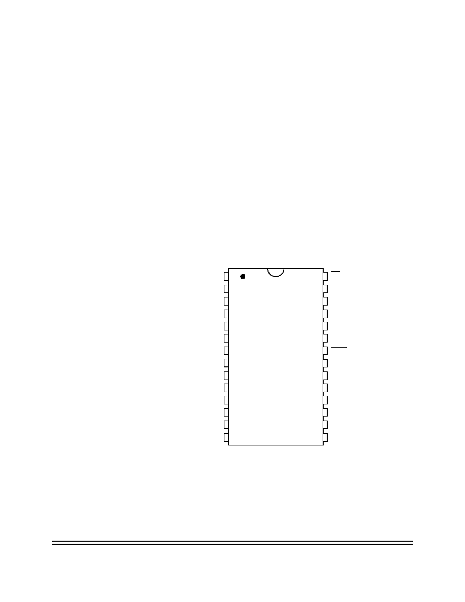
Figure 1-2
shows the 28-pin SOIC pin assignments.
Figure 1-2 MC68HC(8)05PV8/A Pin Assignments
1
PA0/VREFL
PA1/AN1
PA2/AN2
PA3/AN3
PA5/AN5/IIN
PA6/AN6/IN
PA7/VREFH
VDD
VSUP
PC0/TCAP1/TCMP1/PWM
PC1/TCMP1
2
3
4
5
6
7
8
9
10
11
12
13
14
PA4/AN4/OUT
PC2/TCAP2
PC3/TCMP2
28
PB0/TCAP1
PB1/TCMP1
PB2/TCAP2
PB4/PWM
RESET
OSC2
OSC1
VSS
PC6/PWM
PVSS
27
26
25
24
23
22
21
20
19
18
17
16
15
PB3/TCMP2
PC5/TCMP1/PWM
PC4/TCMP1/PWM/TCAP1
IRQ
Freescale
Semiconductor,
I
Freescale Semiconductor, Inc.
For More Information On This Product,
Go to: www.freescale.com
nc.
..
Technical Data
Technical Data
MC68HC(8)05PV8/A -- Rev. 1.9
General Description
NO
NDISCLOSURE AGREEMENT REQUIRED
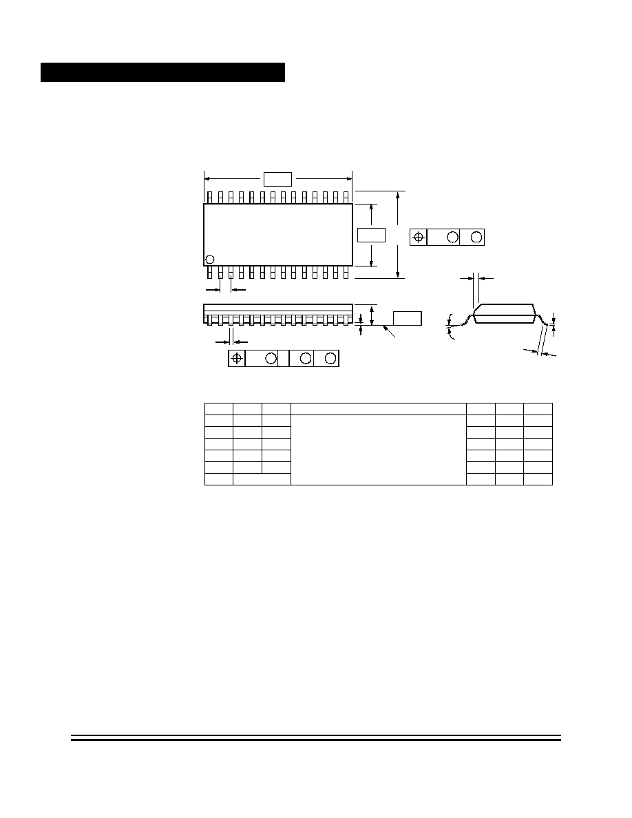
1.6 Mechanical Specifications
Figure 1-3 28-pin SOIC mechanical dimensions
G
D
28 PL
C
K
� T �
Seating
Plane
M
F
J
0.25
M
B M
0.25
M
B
S
A
S
T
14 PL
R x 45
�
1
Dim.
Min.
Max.
Notes
Dim.
Min.
Max.
A
17.80
18.05
1. Dimensions `A' and `B' are datums and `T' is a datum surface.
2. Dimensioning and tolerancing per ANSI Y14.5M, 1982.
3. All dimensions in mm.
4. Dimensions `A' and `B' do not include mould protrusion.
5. Maximum mould protrusion is 0.15 mm per side.
J
0.229
0.317
B
7.40
7.60
K
0.127
0.292
C
2.35
2.65
M
0
�
8
�
D
0.35
0.49
P
10.05
10.55
F
0.41
0.90
R
0.25
0.75
G
1.27 BSC
--
--
--
Case 751F-03
� A �
� B �
P
Freescale
Semiconductor,
I
Freescale Semiconductor, Inc.
For More Information On This Product,
Go to: www.freescale.com
nc.
..

General Description
Functional Pin Descriptions
MC68HC(8)05PV8/A -- Rev. 1.9
Technical Data
General Description
NO
NDI
S
CLO
S
URE AG
REEMENT
REQ
U
IRED
1.7 Functional Pin Descriptions
The following paragraphs give a description of the general function for
each pin.
1.7.1 VSUP, VSS and PVSS
The microcontroller is operated from a single power supply. VSUP is
connected to the positive supply, VSS to ground. The on-chip voltage
regulator uses VSUP to derive the VDD supply for the MCU and external
components. PVSS is a separate ground for the relay drivers.
1.7.2 VDD
This pin is driven by the on-chip voltage regulator. It can be used to
provide a regulated voltage to external devices. A capacitor must be
attached to this pin in order to stabilize the regulator.
1.7.3 OSC1, OSC2
The OSC1 and OSC2 pins are the connections for the on-chip oscillator.
A crystal connected across these pins or an external signal connected to
OSC1 provides the oscillator clock. The frequency, f
OSC
, of the oscillator
or external clock source is divided by two to produce the internal
operating frequency, f
OP
.
1.7.4 RESET
This pin can be used as an input to reset the MCU to a known start-up
state by pulling it to the low state. The RESET pin contains an internal
Schmitt trigger to improve its noise immunity as an input. The RESET pin
has an internal pull-down device that pulls the RESET pin low when
there is an internal COP watchdog reset, power-on reset (POR), illegal
address reset, internal high voltage or an internal low voltage reset.
Refer to
Section 5. Resets
.
Freescale
Semiconductor,
I
Freescale Semiconductor, Inc.
For More Information On This Product,
Go to: www.freescale.com
nc.
..

Technical Data
Technical Data
MC68HC(8)05PV8/A -- Rev. 1.9
General Description
NO
NDISCLOSURE AGREEMENT REQUIRED
1.7.5 IRQ
The interrupt triggering sensitivity of this pin can be programmed as
rising/falling edge sensitive or high/low level sensitive.The IRQ pin
contains an internal Schmitt trigger as part of its input to improve noise
immunity. See
Section 4. Interrupts
for more details on the interrupts.
1.7.6 PA0�PA7/VREFH, VREFL, AN1�6, IN, IIN, OUT
These eight I/O lines comprise port A. The state of any pin is software
programmable and all port A lines are configured as inputs during
power-on or reset. The eight I/O lines are shared with the A/D converter
function (see
Section 10. Analog to Digital Converter
). The internal
operational amplifier is connected to PA4/OUT (output), PA5/IIN
(inverting input) and PA6/IN (input) (see
7.4.6 Operational Amplifier
).
See
Section 7. Input/Output Ports
for more details on the I/O ports.
1.7.7 PB0�PB4/TCMP1, TCMP2, TCAP1, TCAP2, PWM
These five I/O lines comprise port B. The state of any pin is software
programmable and all port B lines are configured as inputs during
power-on or reset. The port pins PB0�PB3 are shared with the 16-bit
timer (TCAP1�2, TCMP1�2). See
Section 9. 16-Bit Programmable
Timer
for more details on the operation of the 16-bit timer. Pin PB4 is
shared with the PWM system (see
Section 11. Pulse Width
Modulator
).
See
Section 7. Input/Output Ports
for more details on the I/O ports.
Freescale
Semiconductor,
I
Freescale Semiconductor, Inc.
For More Information On This Product,
Go to: www.freescale.com
nc.
..

General Description
Ordering Information
MC68HC(8)05PV8/A -- Rev. 1.9
Technical Data
General Description
NO
NDI
S
CLO
S
URE AG
REEMENT
REQ
U
IRED
1.7.8 PTC0�PTC6/TCMP1, TCMP2, TCAP1, TCAP2, PWM
These seven high voltage I/O lines comprise port C. The state of any pin
is software programmable and all port C lines are configured as inputs
during power-on or reset. The port pins PC0�PC5 are shared with the
16-bit timer (TCAP1�2, TCMP1�2). See
Section 9. 16-Bit
Programmable Timer
for more details on the operation of the 16-Bit
Timer. Pins PC0, PC4�6 are shared with the PWM system. PC5�6 are
intended to drive relays.
See
Section 7. Input/Output Ports
for more details on the I/O ports.
1.8 Ordering Information
Table 1-1 Ordering Information
Device
Package Type
Temperature
range
(JUNCTION)
Order Number
(1)
1. The Y in the device order number indicates that this is the junction temperature of the de-
vice, not the ambient temperature.
MC68HC05PV8
28-pin SOIC
�40
�
C to +125
�
C
MC68HC05PV8YDW
MC68HC805PV8
MC68HC805PV8YDW
MC68HC05PV8A
MC68HC05PV8AYDW
Freescale
Semiconductor,
I
Freescale Semiconductor, Inc.
For More Information On This Product,
Go to: www.freescale.com
nc.
..

Technical Data
Technical Data
MC68HC(8)05PV8/A -- Rev. 1.9
General Description
NO
NDISCLOSURE AGREEMENT REQUIRED
Freescale
Semiconductor,
I
Freescale Semiconductor, Inc.
For More Information On This Product,
Go to: www.freescale.com
nc.
..

MC68HC(8)05PV8/A -- Rev. 1.9
Technical Data
Memory
NO
NDI
S
CLO
S
URE AG
REEMENT
REQ
U
IRED
Technical Data -- MC68HC(8)05PV8/A
Section 2. Memory
2.1 Contents
2.2
Introduction . . . . . . . . . . . . . . . . . . . . . . . . . . . . . . . . . . . . . . . . 36
2.3
Registers. . . . . . . . . . . . . . . . . . . . . . . . . . . . . . . . . . . . . . . . . . 37
2.4
RAM . . . . . . . . . . . . . . . . . . . . . . . . . . . . . . . . . . . . . . . . . . . . . 42
2.5
Monitor ROM . . . . . . . . . . . . . . . . . . . . . . . . . . . . . . . . . . . . . . 42
2.6
Program EEPROM/ROM . . . . . . . . . . . . . . . . . . . . . . . . . . . . . 42
2.7
EEPROM . . . . . . . . . . . . . . . . . . . . . . . . . . . . . . . . . . . . . . . . .42
Freescale
Semiconductor,
I
Freescale Semiconductor, Inc.
For More Information On This Product,
Go to: www.freescale.com
nc.
..

Technical Data
Technical Data
MC68HC(8)05PV8/A -- Rev. 1.9
Memory
NO
NDISCLOSURE AGREEMENT REQUIRED
2.2 Introduction
The MC68HC(8)05PV8/A has a 16K byte memory map consisting of
registers (for I/O, control and status), user RAM, user ROM (or program
EEPROM), EEPROM, Monitor ROM, and reset and interrupt vectors as
shown in
Figure 2-1
.
$0000
I/O Registers
32 Bytes
$001F
$0020
I/O Registers
16 Bytes
$002F
$0030
Externally Mapped 4-bit I/O,
If enabled
$003F
$0040
User RAM
192 Bytes
Stack RAM
64 Bytes
$00C0
$00FF
$00FF
$0100
Unused
128 Bytes
$017F
$0180
EEPROM
128 Bytes
$01FF
$0200
Unused
7680 Bytes
$1FFF
$2000
Mask Option Register � 1 Byte
$2001
Program EEPROM/User ROM
7935 Bytes
$3EFF
$3F00
Monitor ROM
240 Bytes
$3FEF
$3FF0
User Vectors
16 Bytes
$3FFF
Figure 2-1 MC68HC(8)05PV8/A Memory Map
Freescale
Semiconductor,
I
Freescale Semiconductor, Inc.
For More Information On This Product,
Go to: www.freescale.com
nc.
..

Memory
Registers
MC68HC(8)05PV8/A -- Rev. 1.9
Technical Data
Memory
NO
NDI
S
CLO
S
URE AG
REEMENT
REQ
U
IRED
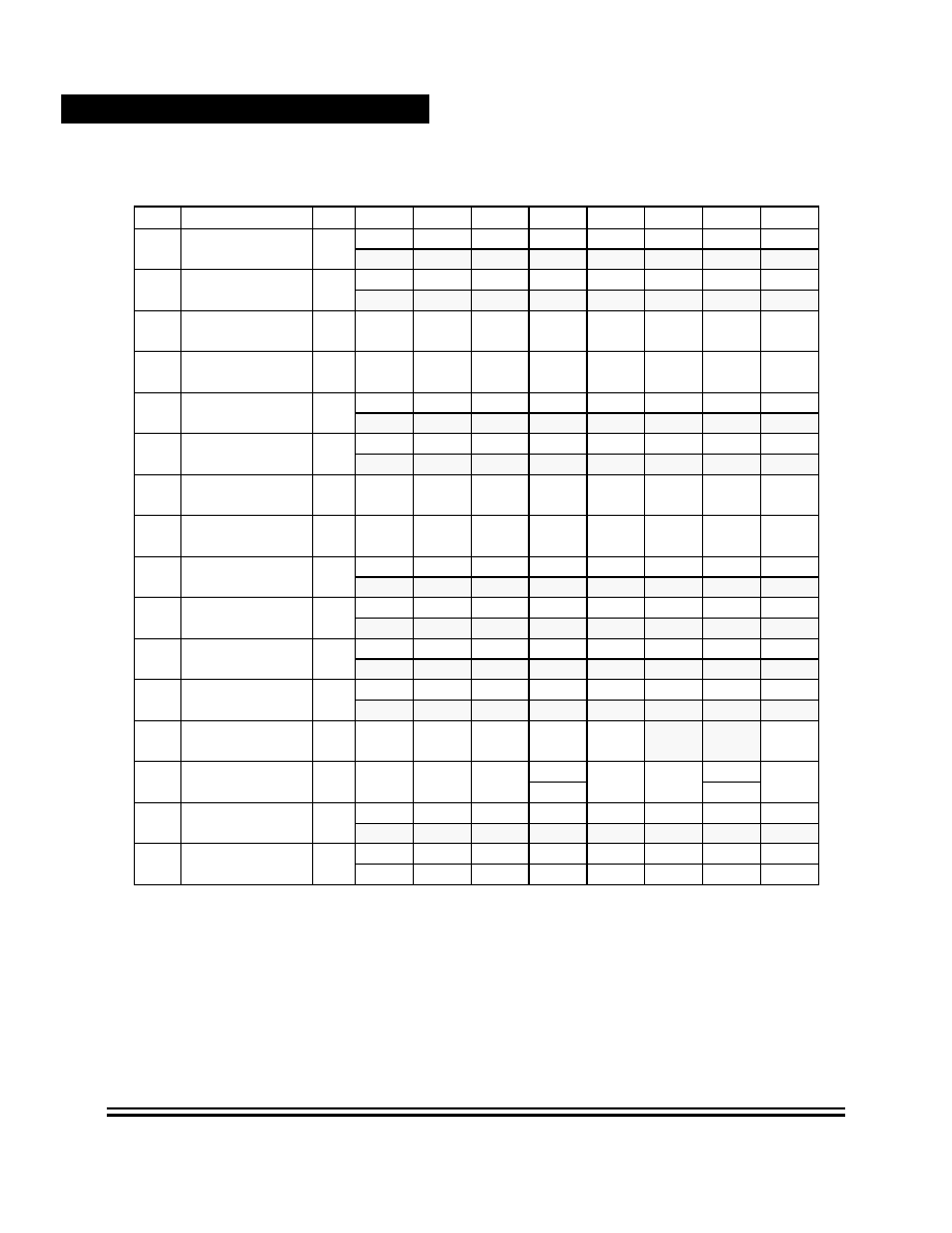
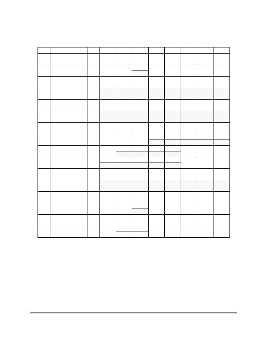
2.3 Registers
The I/O and control registers reside in locations $0000�$002F. The
overall organization of these registers is shown in
Figure 2-2
. The bit
assignments for each register are shown in
Figure 2-3
,
Figure 2-4
and
Figure 2-4
.
Addr
Register Name
$0000
Port A data register
$0001
Port B data register
$0002
Port C data register
$0003
Unused
$0004
Port A data direction register
$0005
Port B data direction register
$0006
Port C data direction register
$0007
Unused
$0008
Core timer control/status (CTCSR)
$0009
Core timer counter (CTCR)
$000A
System control register
$000B
Unused
$000C
EEPROM programming register
$000D
Program EEPROM programming
register
(1)
$000E
A/D data
$000F
A/D status/control
$0010
Timer capture 1 high
$0011
Timer capture 1 low
$0012
Timer compare 1 high
$0013
Timer compare 1 low
$0014
Timer capture 2 high
$0015
Timer capture 2 low
$0016
Timer compare 2 high
$0017
Timer compare 2 low
$0018
Timer counter high
$0019
Timer counter low
$001A
Timer alternate counter high
Figure 2-2 I/O Register Summary
Freescale
Semiconductor,
I
Freescale Semiconductor, Inc.
For More Information On This Product,
Go to: www.freescale.com
nc.
..

Technical Data
Technical Data
MC68HC(8)05PV8/A -- Rev. 1.9
Memory
NO
NDISCLOSURE AGREEMENT REQUIRED
$001B
Timer alternate counter low
$001C
Timer control 1
$001D
Timer control 2
$001E
Timer status
$001F
TEST
$0020
Port A configuration register
$0021
I/O configuration register
$0022
Port C configuration register 0
$0023
Unused
$0024
Port A interrupt status
$0025
Unused
$0026
Port C configuration register 1
$0027
Port C status register
$0028
Interrupt control register
$0029
Interrupt status register
$002A
Reset status register
$002B
Unused
$002C
PWM period
$002D
PWM control
$002E
PWM data
$002F
MFTEST
1. Implemented in MC68HC805PV8 only; unused in
MC68HC05PV8
Addr
Register Name
Figure 2-2 I/O Register Summary
Freescale
Semiconductor,
I
Freescale Semiconductor, Inc.
For More Information On This Product,
Go to: www.freescale.com
nc.
..

Memory
Registers
MC68HC(8)05PV8/A -- Rev. 1.9
Technical Data
Memory
NO
NDI
S
CLO
S
URE AG
REEMENT
REQ
U
IRED
NOTE:
* WCOP Bit is write once
Addr
Register
R/W
Bit 7
6
5
4
3
2
1
Bit 0
$0000
Port A Data
R
PA7
PA6
PA5
PA4
PA3
PA2
PA1
PA0
W
$0001
Port B Data
R
0
0
TCAP1
PB4
PB3
PB2
PB1
PB0
W
$0002
Port C Data
R
0
PC6
PC5
PC4
PC3
PC2
PC1
PC0
W
$0003
Unused
R
W
$0004 Port A Data Direction
R
DDRA7
DDRA6
DDRA5
DDRA4
DDRA3
DDRA2
DDRA1
DDRA0
W
$0005 Port B Data Direction
R
0
0
0
DDRB4
DDRB3
DDRB2
DDRB1
DDRB0
W
$0006 Port C Data Direction
R
0
0
0
DDRC4
DDRC3
DDRC2
DDRC1
DDRC0
W
$0007
Unused
R
W
$0008
CTSCR
R
TOF
RTIF
TOFE
RTIE
0
0
RT1
RT0
W
RTOF
RTIF
$0009
CTCR
R
bit 7
bit 6
bit 5
bit 4
bit 3
bit 2
bit 1
bit 0
W
$000A
System Control
R
POR
INTP
INTN
INTE
WCOP
*
WCP
FPIE
FPICLK
W
$000B
Unused
R
W
$000C
EEPROG
R
0
0
0
EEOSC
EER1
EER0
EELAT
EEPGM
W
$000D
Program EEPROM
Control
R
RCON
BULK
EEPERA EEPLAT EEPPGM
W
$000E
A/D Data
R
bit 7
bit 6
bit 5
bit 4
bit 3
bit 2
bit 1
bit 0
W
$000F
A/D Status/Control
R
COCO
ADRC
ADON
ADTEST
CH3
CH2
CH1
CH0
W
Figure 2-3 I/O Registers $0000�$000F
Freescale
Semiconductor,
I
Freescale Semiconductor, Inc.
For More Information On This Product,
Go to: www.freescale.com
nc.
..
Technical Data
Technical Data
MC68HC(8)05PV8/A -- Rev. 1.9
Memory
NO
NDISCLOSURE AGREEMENT REQUIRED
Addr
Register
R/W
Bit 7
6
5
4
3
2
1
Bit 0
$0010
Timer Input Capture1
High
R
bit 15
bit 14
bit 13
bit 12
bit 11
bit 10
bit 9
bit 8
W
$0011
Timer Input Capture1
Low
R
bit 7
bit 6
bit 5
bit 4
bit 3
bit 2
bit 1
bit 0
W
$0012
Timer Output
Compare1 High
R
bit 15
bit 14
bit 13
bit 12
bit 11
bit 10
bit 9
bit 8
W
$0013
Timer Output
Compare1 Low
R
bit 7
bit 6
bit 5
bit 4
bit 3
bit 2
bit 1
bit 0
W
$0014
Timer Input Capture2
High
R
bit 15
bit 14
bit 13
bit 12
bit 11
bit 10
bit 9
bit 8
W
$0015
Timer Input Capture2
Low
R
bit 7
bit 6
bit 5
bit 4
bit 3
bit 2
bit 1
bit 0
W
$0016
Timer Output
Compare2 High
R
bit 15
bit 14
bit 13
bit 12
bit 11
bit 10
bit 9
bit 8
W
$0017
Timer Output
Compare2 Low
R
bit 7
bit 6
bit 5
bit 4
bit 3
bit 2
bit 1
bit 0
W
$0018
Timer Counter High
R
bit 15
bit 14
bit 13
bit 12
bit 11
bit 10
bit 9
bit 8
W
$0019
Timer Counter Low
R
bit 7
bit 6
bit 5
bit 4
bit 3
bit 2
bit 1
bit 0
W
$001A
Timer Alternate
Counter High
R
bit 15
bit 14
bit 13
bit 12
bit 11
bit 10
bit 9
bit 8
W
$001B
Timer Alternate
Counter Low
R
bit 7
bit 6
bit 5
bit 4
bit 3
bit 2
bit 1
bit 0
W
$001C
Timer Control1
R
ICI1E
ICI2E
OCI1E
TOIE
OCI2E
TOFF
W
$001D
Timer Control2
R
IEDGE1 IEDGE2
CLK21
0
OLVL1
CLK12
0
OLVL2
W
FOLV1
FOLV2
$001E
Timer Status
R
IC1F
IC2F
OC1F
TOF
OC2F
SI1
SI2
0
W
$001F
TEST
R
0
0
0
0
0
0
0
0
W
�
�
�
�
�
�
�
�
Figure 2-4 I/O Registers $0010�$001F
Freescale
Semiconductor,
I
Freescale Semiconductor, Inc.
For More Information On This Product,
Go to: www.freescale.com
nc.
..
Memory
Registers
MC68HC(8)05PV8/A -- Rev. 1.9
Technical Data
Memory
NO
NDI
S
CLO
S
URE AG
REEMENT
REQ
U
IRED
Addr
Register
R/W
Bit 7
6
5
4
3
2
1
Bit 0
$0020 Port A Configuration
R
VRHEN PUHEN EDGEH
PAHIE
PULEN
EDGEL
PALIE
VRLEN
W
$0021
I/O Configuration
R
TXOR
OPAMP
0
PB4PW
PB3OC
PB2IC
PB1OC
PB0IC
W
$0022 Port C Configuration 0
R
ISOM*
PC6PW PWMS1 PWMS0 PC3OC
TS2
TS1
TS0
W
$0023
Unused
R
W
$0024 Port A Interrupt Status
R
PAIF7
PAIF6
PAIF5
PAIF4
PAIF3
PAIF2
PAIF1
PAIF0
W
$0025
Unused
R
W
$0026 Port C Configuration 1
R
CSIE
SCIE6
SCIE5
PC4CS
PC3CS
PC2CS
PC1CS
PC0CS
W
$0027
Port C Status
R
CSIF
SCIF6
SCIF5
CSD4
CSD3
CSD2
CSD1
CSD0
W
$0028
Interrupt Control
Register
R
ULPM
0
0
0
0
HTIE
HVIE
LVIE
W
$0029
Interrupt Status
Register
R
RCON
PC4CL
0
0
0
HTIF
HVIF
LVIF
W
$002A
Reset Status
Register
R
PINR
STOPR
COPR
ILINR
CMR
HTR
HVR
LVR
W
$002B
Unused
R
W
$002C
PWM Period
R
bit 7
bit 6
bit 5
bit 4
bit 3
bit 2
bit 1
bit 0
W
$002D
PWM Control
R
PWMON
POL
0
CYCLE
PRA3
PRA2
PRA1
PRA0
W
$002E
PWM Data
R
bit 7
bit 6
bit 5
bit 4
bit 3
bit 2
bit 1
bit 0
W
$002F
MFTEST
R
HVTOFF
0
0
VSCAL
LSOFF
VT2
VT1
VT0
W
�
�
Figure 2-5 I/O Registers $0020�$002F
NOTE:ISOM bit is without function on 68HC05PV8A
NOTE:ULPM bit is only available on 68HC05PV8A
NOTE:PC4CL is reversed on 68HC05PV8A K20R
Freescale
Semiconductor,
I
Freescale Semiconductor, Inc.
For More Information On This Product,
Go to: www.freescale.com
nc.
..

Technical Data
Technical Data
MC68HC(8)05PV8/A -- Rev. 1.9
Memory
NO
NDISCLOSURE AGREEMENT REQUIRED
2.4 RAM
The user RAM consists of 192 bytes ranging from $0040 to $00FF. The
stack begins at address $00FF. The stack pointer can access 64 bytes
of RAM in the range $00FF to $00C0.
The stack is located in the RAM address space. Data written to
addresses within the stack address range could be overwritten during
stack activity.
2.5 Monitor ROM
The monitor ROM ranges from $3F00 to $3FEF. The vectors for the
bootloader are located from $3FE0 to $3FEF.
2.6 Program EEPROM/ROM
The program EEPROM holds 7952 bytes in total. The mask option
register is located at address $2000. The 7935 bytes of the program
EEPROM are located from $2001 to $3EFF, plus 16 bytes of user
vectors from $3FF0 to $3FFF. The user programs the EEPROM on a 4
byte erase basis by manipulating the programming register located at
address $000D. Refer to
Section 14. Program EEPROM
for details.
This EEPROM is replaced by an 8K ROM in the MC68HC05PV8,
ranging from $2000 to $3EFF and $3FF0 to $3FFF. Mask options are
controlled by the contents of location $2000. Refer to
Section 14.
Program EEPROM
for coding details.
2.7 EEPROM
The 128 bytes of EEPROM are located from $0180 to $01FF. The user
programs the EEPROM on a single-byte basis by manipulating the
programming register, located at address $000C. Refer to
Section 13.
EEPROM
for programming details.
Freescale
Semiconductor,
I
Freescale Semiconductor, Inc.
For More Information On This Product,
Go to: www.freescale.com
nc.
..

MC68HC(8)05PV8/A -- Rev. 1.9
Technical Data
CPU and Instruction Set
NO
NDI
S
CLO
S
URE AG
REEMENT
REQ
U
IRED
Technical Data -- MC68HC(8)05PV8/A
Section 3. CPU and Instruction Set
3.1 Contents
3.2
CPU Registers . . . . . . . . . . . . . . . . . . . . . . . . . . . . . . . . . . . . . 44
3.3
Arithmetic/Logic Unit (ALU) . . . . . . . . . . . . . . . . . . . . . . . . . . .47
3.4
Instruction Set Overview. . . . . . . . . . . . . . . . . . . . . . . . . . . . . .48
3.5
Addressing Modes . . . . . . . . . . . . . . . . . . . . . . . . . . . . . . . . . .48
3.5.1
Inherent . . . . . . . . . . . . . . . . . . . . . . . . . . . . . . . . . . . . . . . . 48
3.5.2
Immediate . . . . . . . . . . . . . . . . . . . . . . . . . . . . . . . . . . . . . . 49
3.5.3
Direct . . . . . . . . . . . . . . . . . . . . . . . . . . . . . . . . . . . . . . . . . . 49
3.5.4
Extended . . . . . . . . . . . . . . . . . . . . . . . . . . . . . . . . . . . . . . . 49
3.5.5
Indexed, No Offset . . . . . . . . . . . . . . . . . . . . . . . . . . . . . . . 49
3.5.6
Indexed, 8-Bit Offset . . . . . . . . . . . . . . . . . . . . . . . . . . . . . . 50
3.5.7
Indexed,16-Bit Offset. . . . . . . . . . . . . . . . . . . . . . . . . . . . . .50
3.5.8
Relative . . . . . . . . . . . . . . . . . . . . . . . . . . . . . . . . . . . . . . . . 50
3.6
Instruction Types . . . . . . . . . . . . . . . . . . . . . . . . . . . . . . . . . . . 51
3.6.1
Register/Memory Instructions . . . . . . . . . . . . . . . . . . . . . . . 52
3.6.2
Read-Modify-Write Instructions . . . . . . . . . . . . . . . . . . . . . . 53
3.6.3
Jump/Branch Instructions . . . . . . . . . . . . . . . . . . . . . . . . . . 54
3.6.4
Bit Manipulation Instructions . . . . . . . . . . . . . . . . . . . . . . . . 56
3.6.5
Control Instructions . . . . . . . . . . . . . . . . . . . . . . . . . . . . . . . 57
3.7
Instruction Set Summary . . . . . . . . . . . . . . . . . . . . . . . . . . . . . 58
Freescale
Semiconductor,
I
Freescale Semiconductor, Inc.
For More Information On This Product,
Go to: www.freescale.com
nc.
..

Technical Data
Technical Data
MC68HC(8)05PV8/A -- Rev. 1.9
CPU and Instruction Set
NO
NDISCLOSURE AGREEMENT REQUIRED
3.2 CPU Registers
Figure 3-1
shows the five CPU registers. CPU registers are not part of
the memory map.
3.2.1 Accumulator
The accumulator is a general-purpose 8-bit register. The CPU uses the
accumulator to hold operands and results of arithmetic and
non-arithmetic operations.
Figure 3-1 Programming Model
ACCUMULATOR (A)
A
INDEX REGISTER (X)
X
SP
1
1
0
0
0
0
0
0
0
0
PCL
PCH
Z
C
I
N
1
H
1
1
0
4
7
5
CONDITION CODE REGISTER (CCR)
PROGRAM COUNTER (PC)
STACK POINTER (SP)
0
7
8
15
15
5
7
7
0
0
0
HALF-CARRY FLAG
INTERRUPT MASK
NEGATIVE FLAG
ZERO FLAG
CARRY/BORROW FLAG
10
6
Bit 7
6
5
4
3
2
1
Bit 0
Reset:
Unaffected by reset
Figure 3-2 Accumulator
Freescale
Semiconductor,
I
Freescale Semiconductor, Inc.
For More Information On This Product,
Go to: www.freescale.com
nc.
..

CPU and Instruction Set
CPU Registers
MC68HC(8)05PV8/A -- Rev. 1.9
Technical Data
CPU and Instruction Set
NO
NDI
S
CLO
S
URE AG
REEMENT
REQ
U
IRED
3.2.2 Index Register
In the indexed addressing modes, the CPU uses the byte in the index
register to determine the conditional address of the operand.
The 8-bit index register can also serve as a temporary data storage
location.
3.2.3 Stack Pointer
The stack pointer is a 16-bit register that contains the address of the next
location on the stack. During a reset or after the reset stack pointer
(RSP) instruction, the stack pointer is preset to $00FF. The address in
the stack pointer decrements as data is pushed onto the stack and
increments as data is pulled from the stack.
The ten most significant bits of the stack pointer are permanently fixed
at 000000011, so the stack pointer produces addresses from $00C0 to
$00FF. If subroutines and interrupts use more than 64 stack locations,
the stack pointer wraps around to address $00FF and begins writing
over the previously stored data. A subroutine uses two stack locations.
An interrupt uses five locations.
Bit 7
6
5
4
3
2
1
Bit 0
Reset:
Unaffected by reset
Figure 3-3 Index Register
Bit 15 14
13
12
11
10
9
8
7
6
5
4
3
2
1
Bit 0
0
0
0
0
0
0
0
0
1
1
Reset
0
0
0
0
0
0
0
0
1
1
1
1
1
1
1
1
Figure 3-4 Stack Pointer
Freescale
Semiconductor,
I
Freescale Semiconductor, Inc.
For More Information On This Product,
Go to: www.freescale.com
nc.
..

Technical Data
Technical Data
MC68HC(8)05PV8/A -- Rev. 1.9
CPU and Instruction Set
NO
NDISCLOSURE AGREEMENT REQUIRED
3.2.4 Program Counter
The program counter is a 16-bit register that contains the address of the
next instruction or operand to be fetched. The two most significant bits
of the program counter are ignored internally.
Normally, the address in the program counter automatically increments
to the next sequential memory location every time an instruction or
operand is fetched. Jump, branch, and interrupt operations load the
program counter with an address other than that of the next sequential
location.
3.2.5 Condition Code Register
The condition code register is an 8-bit register whose three most
significant bits are permanently fixed at 111. The condition code register
contains the interrupt mask and four flags that indicate the results of the
instruction just executed. The following paragraphs describe the
functions of the condition code register.
Half-Carry Flag
The CPU sets the half-carry flag when a carry occurs between bits 3 and
4 of the accumulator during an ADD or ADC operation. The half-carry
flag is required for binary-coded decimal (BCD) arithmetic operations.
Bit 15 14
13
12
11
10
9
8
7
6
5
4
3
2
1
Bit 0
�
�
Reset
�
�
Loaded with vector from $3FFE AND $3FFF
Figure 3-5 Program Counter
Bit 7
6
5
4
3
2
1
Bit 0
1
1
1
H
I
N
C
Z
Reset
1
1
1
U
1
U
U
U
Figure 3-6 Condition Code Register
Freescale
Semiconductor,
I
Freescale Semiconductor, Inc.
For More Information On This Product,
Go to: www.freescale.com
nc.
..

CPU and Instruction Set
Arithmetic/Logic Unit (ALU)
MC68HC(8)05PV8/A -- Rev. 1.9
Technical Data
CPU and Instruction Set
NO
NDI
S
CLO
S
URE AG
REEMENT
REQ
U
IRED
Interrupt Mask
Setting the interrupt mask disables interrupts. If an interrupt request
occurs while the interrupt mask is logic zero, the CPU saves the CPU
registers on the stack, sets the interrupt mask, and then fetches the
interrupt vector. If an interrupt request occurs while the interrupt mask is
set, the interrupt request is latched. Normally, the CPU processes the
latched interrupt as soon as the interrupt mask is cleared again.
A return from interrupt (RTI) instruction pulls the CPU registers from the
stack, restoring the interrupt mask to its cleared state. After any reset,
the interrupt mask is set and can be cleared only by a software
instruction.
Negative Flag
The CPU sets the negative flag when an arithmetic operation, logical
operation, or data manipulation produces a negative result.
Zero Flag
The CPU sets the zero flag when an arithmetic operation, logical
operation, or data manipulation produces a result of $00.
Carry/Borrow Flag
The CPU sets the carry/borrow flag when an addition operation
produces a carry out of bit 7 of the accumulator or when a subtraction
operation requires a borrow. Some logical operations and data
manipulation instructions also clear or set the carry/borrow flag.
3.3 Arithmetic/Logic Unit (ALU)
The ALU performs the arithmetic and logical operations defined by the
instruction set.
The binary arithmetic circuits decode instructions and set up the ALU for
the selected operation. Most binary arithmetic is based on the addition
algorithm, carrying out subtraction as negative addition. Multiplication is
not performed as a discrete operation but as a chain of addition and shift
Freescale
Semiconductor,
I
Freescale Semiconductor, Inc.
For More Information On This Product,
Go to: www.freescale.com
nc.
..

Technical Data
Technical Data
MC68HC(8)05PV8/A -- Rev. 1.9
CPU and Instruction Set
NO
NDISCLOSURE AGREEMENT REQUIRED
operations within the ALU. The multiply instruction (MUL) requires 11
internal clock cycles to complete this chain of operations.
3.4 Instruction Set Overview
The MCU instruction set has 62 instructions and uses eight addressing
modes. The instructions include all those of the M146805 CMOS Family
plus one more: the unsigned multiply (MUL) instruction. The MUL
instruction allows unsigned multiplication of the contents of the
accumulator (A) and the index register (X). The high-order product is
stored in the index register, and the low-order product is stored in the
accumulator.
3.5 Addressing Modes
The CPU uses eight addressing modes for flexibility in accessing data.
The addressing modes provide eight different ways for the CPU to find
the data required to execute an instruction. The eight addressing modes
are:
�
Inherent
�
Immediate
�
Direct
�
Extended
�
Indexed, no offset
�
Indexed, 8-bit offset
�
Indexed, 16-bit offset
�
Relative
3.5.1 Inherent
Inherent instructions are those that have no operand, such as return
from interrupt (RTI) and stop (STOP). Some of the inherent instructions
act on data in the CPU registers, such as set carry flag (SEC) and
Freescale
Semiconductor,
I
Freescale Semiconductor, Inc.
For More Information On This Product,
Go to: www.freescale.com
nc.
..

CPU and Instruction Set
Addressing Modes
MC68HC(8)05PV8/A -- Rev. 1.9
Technical Data
CPU and Instruction Set
NO
NDI
S
CLO
S
URE AG
REEMENT
REQ
U
IRED
increment accumulator (INCA). Inherent instructions require no operand
address and are one byte long.
3.5.2 Immediate
Immediate instructions are those that contain a value to be used in an
operation with the value in the accumulator or index register. Immediate
instructions require no operand address and are two bytes long. The
opcode is the first byte, and the immediate data value is the second byte.
3.5.3 Direct
Direct instructions can access any of the first 256 memory locations with
two bytes. The first byte is the opcode, and the second is the low byte of
the operand address. In direct addressing, the CPU automatically uses
$00 as the high byte of the operand address.
3.5.4 Extended
Extended instructions use three bytes and can access any address in
memory. The first byte is the opcode; the second and third bytes are the
high and low bytes of the operand address.
When using the Motorola assembler, the programmer does not need to
specify whether an instruction is direct or extended. The assembler
automatically selects the shortest form of the instruction.
3.5.5 Indexed, No Offset
Indexed instructions with no offset are 1-byte instructions that can
access data with variable addresses within the first 256 memory
locations. The index register contains the low byte of the effective
address of the operand. The CPU automatically uses $00 as the high
byte, so these instructions can address locations $0000�$00FF.
Indexed, no offset instructions are often used to move a pointer through
a table or to hold the address of a frequently used RAM or I/O location.
Freescale
Semiconductor,
I
Freescale Semiconductor, Inc.
For More Information On This Product,
Go to: www.freescale.com
nc.
..

Technical Data
Technical Data
MC68HC(8)05PV8/A -- Rev. 1.9
CPU and Instruction Set
NO
NDISCLOSURE AGREEMENT REQUIRED
3.5.6 Indexed, 8-Bit Offset
Indexed, 8-bit offset instructions are 2-byte instructions that can access
data with variable addresses within the first 511 memory locations. The
CPU adds the unsigned byte in the index register to the unsigned byte
following the opcode. The sum is the effective address of the operand.
These instructions can access locations $0000�$01FE.
Indexed 8-bit offset instructions are useful for selecting the kth element
in an n-element table. The table can begin anywhere within the first 256
memory locations and could extend as far as location 510 ($01FE). The
k value is typically in the index register, and the address of the beginning
of the table is in the byte following the opcode.
3.5.7 Indexed,16-Bit Offset
Indexed, 16-bit offset instructions are 3-byte instructions that can access
data with variable addresses at any location in memory. The CPU adds
the unsigned byte in the index register to the two unsigned bytes
following the opcode. The sum is the effective address of the operand.
The first byte after the opcode is the high byte of the 16-bit offset; the
second byte is the low byte of the offset.
Indexed, 16-bit offset instructions are useful for selecting the kth element
in an n-element table anywhere in memory.
As with direct and extended addressing, the Motorola assembler
determines the shortest form of indexed addressing.
3.5.8 Relative
Relative addressing is only for branch instructions. If the branch
condition is true, the CPU finds the effective branch destination by
adding the signed byte following the opcode to the contents of the
program counter. If the branch condition is not true, the CPU goes to the
next instruction. The offset is a signed, two's complement byte that gives
a branching range of �128 to +127 bytes from the address of the next
location after the branch instruction.
Freescale
Semiconductor,
I
Freescale Semiconductor, Inc.
For More Information On This Product,
Go to: www.freescale.com
nc.
..

CPU and Instruction Set
Instruction Types
MC68HC(8)05PV8/A -- Rev. 1.9
Technical Data
CPU and Instruction Set
NO
NDI
S
CLO
S
URE AG
REEMENT
REQ
U
IRED
When using the Motorola assembler, the programmer does not need to
calculate the offset, because the assembler determines the proper offset
and verifies that it is within the span of the branch.
3.6 Instruction Types
The MCU instructions fall into the following five categories:
�
Register/Memory Instructions
�
Read-Modify-Write Instructions
�
Jump/Branch Instructions
�
Bit Manipulation Instructions
�
Control Instructions
Freescale
Semiconductor,
I
Freescale Semiconductor, Inc.
For More Information On This Product,
Go to: www.freescale.com
nc.
..

Technical Data
Technical Data
MC68HC(8)05PV8/A -- Rev. 1.9
CPU and Instruction Set
NO
NDISCLOSURE AGREEMENT REQUIRED
3.6.1 Register/Memory Instructions
These instructions operate on CPU registers and memory locations.
Most of them use two operands. One operand is in either the
accumulator or the index register. The CPU finds the other operand in
memory.
Table 3-1 Register/Memory Instructions
Instruction
Mnemonic
Add Memory Byte and Carry Bit to Accumulator
ADC
Add Memory Byte to Accumulator
ADD
AND Memory Byte with Accumulator
AND
Bit Test Accumulator
BIT
Compare Accumulator
CMP
Compare Index Register with Memory Byte
CPX
EXCLUSIVE OR Accumulator with Memory Byte
EOR
Load Accumulator with Memory Byte
LDA
Load Index Register with Memory Byte
LDX
Multiply
MUL
OR Accumulator with Memory Byte
ORA
Subtract Memory Byte and Carry Bit from Accumulator
SBC
Store Accumulator in Memory
STA
Store Index Register in Memory
STX
Subtract Memory Byte from Accumulator
SUB
Freescale
Semiconductor,
I
Freescale Semiconductor, Inc.
For More Information On This Product,
Go to: www.freescale.com
nc.
..

CPU and Instruction Set
Instruction Types
MC68HC(8)05PV8/A -- Rev. 1.9
Technical Data
CPU and Instruction Set
NO
NDI
S
CLO
S
URE AG
REEMENT
REQ
U
IRED
3.6.2 Read-Modify-Write Instructions
These instructions read a memory location or a register, modify its
contents, and write the modified value back to the memory location or to
the register.
NOTE:
Do not use read-modify-write operations on write-only registers.
Table 3-2 Read-Modify-Write Instructions
Instruction
Mnemonic
Arithmetic Shift Left (Same as LSL)
ASL
Arithmetic Shift Right
ASR
Bit Clear
BCLR
(1)
1. Unlike other read-modify-write instructions, BCLR and
BSET use only direct addressing.
Bit Set
BSET
(1)
Clear Register
CLR
Complement (One's Complement)
COM
Decrement
DEC
Increment
INC
Logical Shift Left (Same as ASL)
LSL
Logical Shift Right
LSR
Negate (Two's Complement)
NEG
Rotate Left through Carry Bit
ROL
Rotate Right through Carry Bit
ROR
Test for Negative or Zero
TST
(2)
2. TST is an exception to the read-modify-write sequence be-
cause it does not write a replacement value.
Freescale
Semiconductor,
I
Freescale Semiconductor, Inc.
For More Information On This Product,
Go to: www.freescale.com
nc.
..

Technical Data
Technical Data
MC68HC(8)05PV8/A -- Rev. 1.9
CPU and Instruction Set
NO
NDISCLOSURE AGREEMENT REQUIRED
3.6.3 Jump/Branch Instructions
Jump instructions allow the CPU to interrupt the normal sequence of the
program counter. The unconditional jump instruction (JMP) and the
jump-to-subroutine instruction (JSR) have no register operand. Branch
instructions allow the CPU to interrupt the normal sequence of the
program counter when a test condition is met. If the test condition is not
met, the branch is not performed.
The BRCLR and BRSET instructions cause a branch based on the state
of any readable bit in the first 256 memory locations. These 3-byte
instructions use a combination of direct addressing and relative
addressing. The direct address of the byte to be tested is in the byte
following the opcode. The third byte is the signed offset byte. The CPU
finds the effective branch destination by adding the third byte to the
program counter if the specified bit tests true. The bit to be tested and its
condition (set or clear) is part of the opcode. The span of branching is
from �128 to +127 from the address of the next location after the branch
instruction. The CPU also transfers the tested bit to the carry/borrow bit
of the condition code register.
Freescale
Semiconductor,
I
Freescale Semiconductor, Inc.
For More Information On This Product,
Go to: www.freescale.com
nc.
..

CPU and Instruction Set
Instruction Types
MC68HC(8)05PV8/A -- Rev. 1.9
Technical Data
CPU and Instruction Set
NO
NDI
S
CLO
S
URE AG
REEMENT
REQ
U
IRED
Table 3-3 Jump and Branch Instructions
Instruction
Mnemonic
Branch if Carry Bit Clear
BCC
Branch if Carry Bit Set
BCS
Branch if Equal
BEQ
Branch if Half-Carry Bit Clear
BHCC
Branch if Half-Carry Bit Set
BHCS
Branch if Higher
BHI
Branch if Higher or Same
BHS
Branch if IRQ Pin High
BIH
Branch if IRQ Pin Low
BIL
Branch if Lower
BLO
Branch if Lower or Same
BLS
Branch if Interrupt Mask Clear
BMC
Branch if Minus
BMI
Branch if Interrupt Mask Set
BMS
Branch if Not Equal
BNE
Branch if Plus
BPL
Branch Always
BRA
Branch if Bit Clear
BRCLR
Branch Never
BRN
Branch if Bit Set
BRSET
Branch to Subroutine
BSR
Unconditional Jump
JMP
Jump to Subroutine
JSR
Freescale
Semiconductor,
I
Freescale Semiconductor, Inc.
For More Information On This Product,
Go to: www.freescale.com
nc.
..

Technical Data
Technical Data
MC68HC(8)05PV8/A -- Rev. 1.9
CPU and Instruction Set
NO
NDISCLOSURE AGREEMENT REQUIRED
3.6.4 Bit Manipulation Instructions
The CPU can set or clear any writable bit in the first 256 bytes of
memory, which includes I/O registers and on-chip RAM locations. The
CPU can also test and branch based on the state of any bit in any of the
first 256 memory locations.
Table 3-4 Bit Manipulation Instructions
Instruction
Mnemonic
Bit Clear
BCLR
Branch if Bit Clear
BRCLR
Branch if Bit Set
BRSET
Bit Set
BSET
Freescale
Semiconductor,
I
Freescale Semiconductor, Inc.
For More Information On This Product,
Go to: www.freescale.com
nc.
..

CPU and Instruction Set
Instruction Types
MC68HC(8)05PV8/A -- Rev. 1.9
Technical Data
CPU and Instruction Set
NO
NDI
S
CLO
S
URE AG
REEMENT
REQ
U
IRED
3.6.5 Control Instructions
These instructions act on CPU registers and control CPU operation
during program execution.
Table 3-5 Control Instructions
Instruction
Mnemonic
Clear Carry Bit
CLC
Clear Interrupt Mask
CLI
No Operation
NOP
Reset Stack Pointer
RSP
Return from Interrupt
RTI
Return from Subroutine
RTS
Set Carry Bit
SEC
Set Interrupt Mask
SEI
Stop Oscillator and Enable IRQ Pin
STOP
Software Interrupt
SWI
Transfer Accumulator to Index Register
TAX
Transfer Index Register to Accumulator
TXA
Stop CPU Clock and Enable Interrupts
WAIT
Freescale
Semiconductor,
I
Freescale Semiconductor, Inc.
For More Information On This Product,
Go to: www.freescale.com
nc.
..
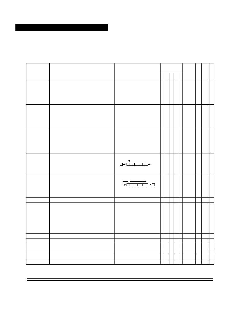
Technical Data
Technical Data
MC68HC(8)05PV8/A -- Rev. 1.9
CPU and Instruction Set
NO
NDISCLOSURE AGREEMENT REQUIRED
3.7 Instruction Set Summary
Table 3-6 Instruction Set Summary
Source
Form
Operation
Description
Effect on
CCR
Addr
e
s
s
Mo
d
e
Opc
ode
Op
e
r
a
n
d
Cycl
es
H I N Z C
ADC #opr
ADC opr
ADC opr
ADC opr,X
ADC opr,X
ADC ,X
Add with Carry
A
(A) + (M) + (C)
--
IMM
DIR
EXT
IX2
IX1
IX
A9
B9
C9
D9
E9
F9
ii
dd
hh ll
ee ff
ff
2
3
4
5
4
3
ADD #opr
ADD opr
ADD opr
ADD opr,X
ADD opr,X
ADD ,X
Add without Carry
A
(A) + (M)
--
IMM
DIR
EXT
IX2
IX1
IX
AB
BB
CB
DB
EB
FB
ii
dd
hh ll
ee ff
ff
2
3
4
5
4
3
AND #opr
AND opr
AND opr
AND opr,X
AND opr,X
AND ,X
Logical AND
A
(A)
(M)
-- --
--
IMM
DIR
EXT
IX2
IX1
IX
A4
B4
C4
D4
E4
F4
ii
dd
hh ll
ee ff
ff
2
3
4
5
4
3
ASL opr
ASLA
ASLX
ASL opr,X
ASL ,X
Arithmetic Shift Left (Same as LSL)
-- --
DIR
INH
INH
IX1
IX
38
48
58
68
78
dd
ff
5
3
3
6
5
ASR opr
ASRA
ASRX
ASR opr,X
ASR ,X
Arithmetic Shift Right
-- --
DIR
INH
INH
IX1
IX
37
47
57
67
77
dd
ff
5
3
3
6
5
BCC rel
Branch if Carry Bit Clear
PC
(PC) + 2 + rel ? C = 0
-- -- -- -- --
REL
24
rr
3
BCLR n opr
Clear Bit n
Mn
0
-- -- -- -- --
DIR (b0)
DIR (b1)
DIR (b2)
DIR (b3)
DIR (b4)
DIR (b5)
DIR (b6)
DIR (b7)
11
13
15
17
19
1B
1D
1F
dd
dd
dd
dd
dd
dd
dd
dd
5
5
5
5
5
5
5
5
BCS rel
Branch if Carry Bit Set (Same as BLO)
PC
(PC) + 2 + rel ? C = 1
-- -- -- -- --
REL
25
rr
3
BEQ rel
Branch if Equal
PC
(PC) + 2 + rel ? Z = 1
-- -- -- -- --
REL
27
rr
3
BHCC rel
Branch if Half-Carry Bit Clear
PC
(PC) + 2 + rel ? H = 0
-- -- -- -- --
REL
28
rr
3
BHCS rel
Branch if Half-Carry Bit Set
PC
(PC) + 2 + rel ? H = 1
-- -- -- -- --
REL
29
rr
3
BHI rel
Branch if Higher
PC
(PC) + 2 + rel ? C
Z = 0
-- -- -- -- --
REL
22
rr
3
BHS rel
Branch if Higher or Same
PC
(PC) + 2 + rel ? C = 0
-- -- -- -- --
REL
24
rr
3
C
b0
b7
0
b0
b7
C
Freescale
Semiconductor,
I
Freescale Semiconductor, Inc.
For More Information On This Product,
Go to: www.freescale.com
nc.
..

CPU and Instruction Set
Instruction Set Summary
MC68HC(8)05PV8/A -- Rev. 1.9
Technical Data
CPU and Instruction Set
NO
NDI
S
CLO
S
URE AG
REEMENT
REQ
U
IRED
BIH rel
Branch if IRQ Pin High
PC
(PC) + 2 + rel ? IRQ = 1
-- -- -- -- --
REL
2F
rr
3
BIL rel
Branch if IRQ Pin Low
PC
(PC) + 2 + rel ? IRQ = 0
-- -- -- -- --
REL
2E
rr
3
BIT #opr
BIT opr
BIT opr
BIT opr,X
BIT opr,X
BIT ,X
Bit Test Accumulator with Memory Byte
(A)
(M)
-- --
--
IMM
DIR
EXT
IX2
IX1
IX
A5
B5
C5
D5
E5
F5
ii
dd
hh ll
ee ff
ff
2
3
4
5
4
3
BLO rel
Branch if Lower (Same as BCS)
PC
(PC) + 2 + rel ? C = 1
-- -- -- -- --
REL
25
rr
3
BLS rel
Branch if Lower or Same
PC
(PC) + 2 + rel ? C
Z = 1
-- -- -- -- --
REL
23
rr
3
BMC rel
Branch if Interrupt Mask Clear
PC
(PC) + 2 + rel ? I = 0
-- -- -- -- --
REL
2C
rr
3
BMI rel
Branch if Minus
PC
(PC) + 2 + rel ? N = 1
-- -- -- -- --
REL
2B
rr
3
BMS rel
Branch if Interrupt Mask Set
PC
(PC) + 2 + rel ? I = 1
-- -- -- -- --
REL
2D
rr
3
BNE rel
Branch if Not Equal
PC
(PC) + 2 + rel ? Z = 0
-- -- -- -- --
REL
26
rr
3
BPL rel
Branch if Plus
PC
(PC) + 2 + rel ? N = 0
-- -- -- -- --
REL
2A
rr
3
BRA rel
Branch Always
PC
(PC) + 2 + rel ? 1 = 1
-- -- -- -- --
REL
20
rr
3
BRCLR n opr rel Branch if Bit n Clear
PC
(PC) + 2 + rel ? Mn = 0
-- -- -- --
DIR (b0)
DIR (b1)
DIR (b2)
DIR (b3)
DIR (b4)
DIR (b5)
DIR (b6)
DIR (b7)
01
03
05
07
09
0B
0D
0F
dd rr
dd rr
dd rr
dd rr
dd rr
dd rr
dd rr
dd rr
5
5
5
5
5
5
5
5
BRN rel
Branch Never
PC
(PC) + 2 + rel ? 1 = 0
-- -- -- -- --
REL
21
rr
3
BRSET n opr rel Branch if Bit n Set
PC
(PC) + 2 + rel ? Mn = 1
-- -- -- --
DIR (b0)
DIR (b1)
DIR (b2)
DIR (b3)
DIR (b4)
DIR (b5)
DIR (b6)
DIR (b7)
00
02
04
06
08
0A
0C
0E
dd rr
dd rr
dd rr
dd rr
dd rr
dd rr
dd rr
dd rr
5
5
5
5
5
5
5
5
BSET n opr
Set Bit n
Mn
1
-- -- -- -- --
DIR (b0)
DIR (b1)
DIR (b2)
DIR (b3)
DIR (b4)
DIR (b5)
DIR (b6)
DIR (b7)
10
12
14
16
18
1A
1C
1E
dd
dd
dd
dd
dd
dd
dd
dd
5
5
5
5
5
5
5
5
BSR rel
Branch to Subroutine
PC
(PC) + 2; push (PCL)
SP
(SP) � 1; push (PCH)
SP
(SP) � 1
PC
(PC) + rel
-- -- -- -- --
REL
AD
rr
6
CLC
Clear Carry Bit
C
0
-- -- -- -- 0
INH
98
2
CLI
Clear Interrupt Mask
I
0
-- 0 -- -- --
INH
9A
2
Table 3-6 Instruction Set Summary (Continued)
Source
Form
Operation
Description
Effect on
CCR
Addr
e
s
s
Mo
d
e
Opc
ode
Op
e
r
a
n
d
Cycl
es
H I N Z C
Freescale
Semiconductor,
I
Freescale Semiconductor, Inc.
For More Information On This Product,
Go to: www.freescale.com
nc.
..
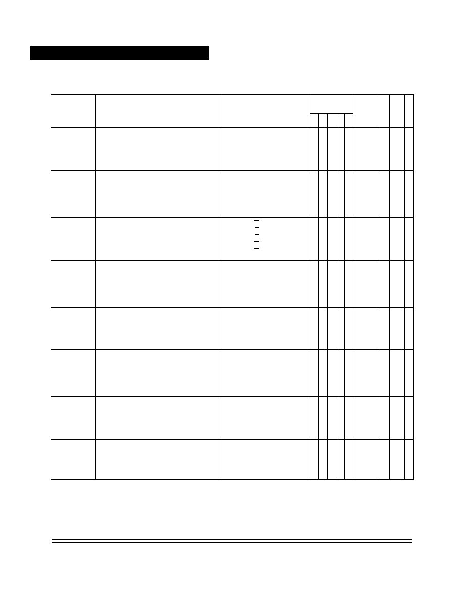
Technical Data
Technical Data
MC68HC(8)05PV8/A -- Rev. 1.9
CPU and Instruction Set
NO
NDISCLOSURE AGREEMENT REQUIRED
CLR opr
CLRA
CLRX
CLR opr,X
CLR ,X
Clear Byte
M
$00
A
$00
X
$00
M
$00
M
$00
-- -- 0
1 --
DIR
INH
INH
IX1
IX
3F
4F
5F
6F
7F
dd
ff
5
3
3
6
5
CMP #opr
CMP opr
CMP opr
CMP opr,X
CMP opr,X
CMP ,X
Compare Accumulator with Memory Byte
(A) � (M)
-- --
IMM
DIR
EXT
IX2
IX1
IX
A1
B1
C1
D1
E1
F1
ii
dd
hh ll
ee ff
ff
2
3
4
5
4
3
COM opr
COMA
COMX
COM opr,X
COM ,X
Complement Byte (One's Complement)
M
(M) = $FF � (M)
A
(A) = $FF � (A)
X
(X) = $FF � (X)
M
(M) = $FF � (M)
M
(M) = $FF � (M)
-- --
1
DIR
INH
INH
IX1
IX
33
43
53
63
73
dd
ff
5
3
3
6
5
CPX #opr
CPX opr
CPX opr
CPX opr,X
CPX opr,X
CPX ,X
Compare Index Register with Memory Byte
(X) � (M)
-- --
IMM
DIR
EXT
IX2
IX1
IX
A3
B3
C3
D3
E3
F3
ii
dd
hh ll
ee ff
ff
2
3
4
5
4
3
DEC opr
DECA
DECX
DEC opr,X
DEC ,X
Decrement Byte
M
(M) � 1
A
(A) � 1
X
(X) � 1
M
(M) � 1
M
(M) � 1
-- --
--
DIR
INH
INH
IX1
IX
3A
4A
5A
6A
7A
dd
ff
5
3
3
6
5
EOR #opr
EOR opr
EOR opr
EOR opr,X
EOR opr,X
EOR ,X
EXCLUSIVE OR Accumulator with Memory Byte
A
(A)
(M)
-- --
--
IMM
DIR
EXT
IX2
IX1
IX
A8
B8
C8
D8
E8
F8
ii
dd
hh ll
ee ff
ff
2
3
4
5
4
3
INC opr
INCA
INCX
INC opr,X
INC ,X
Increment Byte
M
(M) + 1
A
(A) + 1
X
(X) + 1
M
(M) + 1
M
(M) + 1
-- --
--
DIR
INH
INH
IX1
IX
3C
4C
5C
6C
7C
dd
ff
5
3
3
6
5
JMP opr
JMP opr
JMP opr,X
JMP opr,X
JMP ,X
Unconditional Jump
PC
Jump Address
-- -- -- -- --
DIR
EXT
IX2
IX1
IX
BC
CC
DC
EC
FC
dd
hh ll
ee ff
ff
2
3
4
3
2
Table 3-6 Instruction Set Summary (Continued)
Source
Form
Operation
Description
Effect on
CCR
Addr
e
s
s
Mo
d
e
Opc
ode
Op
e
r
a
n
d
Cycl
es
H I N Z C
Freescale
Semiconductor,
I
Freescale Semiconductor, Inc.
For More Information On This Product,
Go to: www.freescale.com
nc.
..

CPU and Instruction Set
Instruction Set Summary
MC68HC(8)05PV8/A -- Rev. 1.9
Technical Data
CPU and Instruction Set
NO
NDI
S
CLO
S
URE AG
REEMENT
REQ
U
IRED
JSR opr
JSR opr
JSR opr,X
JSR opr,X
JSR ,X
Jump to Subroutine
PC
(PC) + n (n = 1, 2, or 3)
Push (PCL); SP
(SP) � 1
Push (PCH); SP
(SP) � 1
PC
Effective Address
-- -- -- -- --
DIR
EXT
IX2
IX1
IX
BD
CD
DD
ED
FD
dd
hh ll
ee ff
ff
5
6
7
6
5
LDA #opr
LDA opr
LDA opr
LDA opr,X
LDA opr,X
LDA ,X
Load Accumulator with Memory Byte
A
(M)
-- --
--
IMM
DIR
EXT
IX2
IX1
IX
A6
B6
C6
D6
E6
F6
ii
dd
hh ll
ee ff
ff
2
3
4
5
4
3
LDX #opr
LDX opr
LDX opr
LDX opr,X
LDX opr,X
LDX ,X
Load Index Register with Memory Byte
X
(M)
-- --
--
IMM
DIR
EXT
IX2
IX1
IX
AE
BE
CE
DE
EE
FE
ii
dd
hh ll
ee ff
ff
2
3
4
5
4
3
LSL opr
LSLA
LSLX
LSL opr,X
LSL ,X
Logical Shift Left (Same as ASL)
-- --
DIR
INH
INH
IX1
IX
38
48
58
68
78
dd
ff
5
3
3
6
5
LSR opr
LSRA
LSRX
LSR opr,X
LSR ,X
Logical Shift Right
-- -- 0
DIR
INH
INH
IX1
IX
34
44
54
64
74
dd
ff
5
3
3
6
5
MUL
Unsigned Multiply
X : A
(X)
�
(A)
0 -- -- -- 0
INH
42
11
NEG opr
NEGA
NEGX
NEG opr,X
NEG ,X
Negate Byte (Two's Complement)
M
�(M) = $00 � (M)
A
�(A) = $00 � (A)
X
�(X) = $00 � (X)
M
�(M) = $00 � (M)
M
�(M) = $00 � (M)
-- --
DIR
INH
INH
IX1
IX
30
40
50
60
70
dd
ff
5
3
3
6
5
NOP
No Operation
-- -- -- -- --
INH
9D
2
ORA #opr
ORA opr
ORA opr
ORA opr,X
ORA opr,X
ORA ,X
Logical OR Accumulator with Memory
A
(A)
(M)
-- --
--
IMM
DIR
EXT
IX2
IX1
IX
AA
BA
CA
DA
EA
FA
ii
dd
hh ll
ee ff
ff
2
3
4
5
4
3
ROL opr
ROLA
ROLX
ROL opr,X
ROL ,X
Rotate Byte Left through Carry Bit
-- --
DIR
INH
INH
IX1
IX
39
49
59
69
79
dd
ff
5
3
3
6
5
Table 3-6 Instruction Set Summary (Continued)
Source
Form
Operation
Description
Effect on
CCR
Addr
e
s
s
Mo
d
e
Opc
ode
Op
e
r
a
n
d
Cycl
es
H I N Z C
C
b0
b7
0
b0
b7
C
0
C
b0
b7
Freescale
Semiconductor,
I
Freescale Semiconductor, Inc.
For More Information On This Product,
Go to: www.freescale.com
nc.
..

Technical Data
Technical Data
MC68HC(8)05PV8/A -- Rev. 1.9
CPU and Instruction Set
NO
NDISCLOSURE AGREEMENT REQUIRED
ROR opr
RORA
RORX
ROR opr,X
ROR ,X
Rotate Byte Right through Carry Bit
-- --
DIR
INH
INH
IX1
IX
36
46
56
66
76
dd
ff
5
3
3
6
5
RSP
Reset Stack Pointer
SP
$00FF
-- -- -- -- --
INH
9C
2
RTI
Return from Interrupt
SP
(SP) + 1; Pull (CCR)
SP
(SP) + 1; Pull (A)
SP
(SP) + 1; Pull (X)
SP
(SP) + 1; Pull (PCH)
SP
(SP) + 1; Pull (PCL)
INH
80
9
RTS
Return from Subroutine
SP
(SP) + 1; Pull (PCH)
SP
(SP) + 1; Pull (PCL)
-- -- -- -- --
INH
81
6
SBC #opr
SBC opr
SBC opr
SBC opr,X
SBC opr,X
SBC ,X
Subtract Memory Byte and Carry Bit from
Accumulator
A
(A) � (M) � (C)
-- --
IMM
DIR
EXT
IX2
IX1
IX
A2
B2
C2
D2
E2
F2
ii
dd
hh ll
ee ff
ff
2
3
4
5
4
3
SEC
Set Carry Bit
C
1
-- -- -- -- 1
INH
99
2
SEI
Set Interrupt Mask
I
1
-- 1 -- -- --
INH
9B
2
STA opr
STA opr
STA opr,X
STA opr,X
STA ,X
Store Accumulator in Memory
M
(A)
-- --
--
DIR
EXT
IX2
IX1
IX
B7
C7
D7
E7
F7
dd
hh ll
ee ff
ff
4
5
6
5
4
STOP
Stop Oscillator and Enable IRQ Pin
-- 0 -- -- --
INH
8E
2
STX opr
STX opr
STX opr,X
STX opr,X
STX ,X
Store Index Register In Memory
M
(X)
-- --
--
DIR
EXT
IX2
IX1
IX
BF
CF
DF
EF
FF
dd
hh ll
ee ff
ff
4
5
6
5
4
SUB #opr
SUB opr
SUB opr
SUB opr,X
SUB opr,X
SUB ,X
Subtract Memory Byte from Accumulator
A
(A) � (M)
-- --
IMM
DIR
EXT
IX2
IX1
IX
A0
B0
C0
D0
E0
F0
ii
dd
hh ll
ee ff
ff
2
3
4
5
4
3
SWI
Software Interrupt
PC
(PC) + 1; Push (PCL)
SP
(SP) � 1; Push (PCH)
SP
(SP) � 1; Push (X)
SP
(SP) � 1; Push (A)
SP
(SP) � 1; Push (CCR)
SP
(SP) � 1; I
1
PCH
Interrupt Vector High Byte
PCL
Interrupt Vector Low Byte
-- 1 -- -- --
INH
83
10
TAX
Transfer Accumulator to Index Register
X
(A)
-- -- -- -- --
INH
97
2
Table 3-6 Instruction Set Summary (Continued)
Source
Form
Operation
Description
Effect on
CCR
Addr
e
s
s
Mo
d
e
Opc
ode
Op
e
r
a
n
d
Cycl
es
H I N Z C
b0
b7
C
Freescale
Semiconductor,
I
Freescale Semiconductor, Inc.
For More Information On This Product,
Go to: www.freescale.com
nc.
..
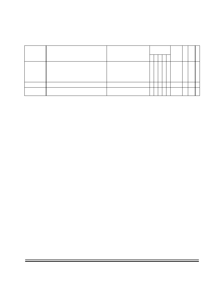
CPU and Instruction Set
Instruction Set Summary
MC68HC(8)05PV8/A -- Rev. 1.9
Technical Data
CPU and Instruction Set
NO
NDI
S
CLO
S
URE AG
REEMENT
REQ
U
IRED
TST opr
TSTA
TSTX
TST opr,X
TST ,X
Test Memory Byte for Negative or Zero
(M) � $00
-- --
--
DIR
INH
INH
IX1
IX
3D
4D
5D
6D
7D
dd
ff
4
3
3
5
4
TXA
Transfer Index Register to Accumulator
A
(X)
-- -- -- -- --
INH
9F
2
WAIT
Stop CPU Clock and Enable Interrupts
--
0
-- -- --
INH
8F
2
A Accumulatoropr
Operand (one or two bytes)
C Carry/borrow flagPC
Program counter
CCRCondition code registerPCH
Program counter high byte
ddDirect address of operandPCL
Program counter low byte
dd rrDirect address of operand and relative offset of branch instructionREL
Relative addressing mode
DIRDirect addressing moderel
Relative program counter offset byte
ee ffHigh and low bytes of offset in indexed, 16-bit offset addressingrr
Relative program counter offset byte
EXTExtended addressing modeSP
Stack pointer
ff Offset byte in indexed, 8-bit offset addressingX
Index register
H Half-carry flagZ
Zero flag
hh llHigh and low bytes of operand address in extended addressing#
Immediate value
I Interrupt mask
Logical AND
ii Immediate operand byte
Logical OR
IMMImmediate addressing mode
Logical EXCLUSIVE OR
INHInherent addressing mode( )
Contents of
IXIndexed, no offset addressing mode�( )
Negation (two's complement)
IX1Indexed, 8-bit offset addressing mode
Loaded with
IX2Indexed, 16-bit offset addressing mode?
If
MMemory location:
Concatenated with
N Negative flag
Set or cleared
n Any bit--
Not affected
Table 3-6 Instruction Set Summary (Continued)
Source
Form
Operation
Description
Effect on
CCR
Addr
e
s
s
Mo
d
e
Opc
ode
Op
e
r
a
n
d
Cycl
es
H I N Z C
Freescale
Semiconductor,
I
Freescale Semiconductor, Inc.
For More Information On This Product,
Go to: www.freescale.com
nc.
..

Technical Data
Instruction Set Summary
Technical Data
MC68HC(8)05PV8/A -- Rev. 1.9
CPU and Instruction Set
NO
ND
ISCLO
SURE AG
REEME
N
T
REQ
UIRED
T
a
ble
3-
7 Op
code
Map
Bit
M
a
ni
pul
a
t
i
on
Br
a
n
c
h
Re
a
d
-
M
od
if
y
-
Wr
it
e
C
on
t
r
ol
Re
gis
t
e
r
/
M
e
m
or
y
D
I
R
D
IR
R
E
L
D
IR
IN
H
I
N
H
IX
1
I
X
I
N
H
IN
H
I
M
M
D
I
R
E
XT
I
X
2
I
X
1
IX
01
234
567
89
A
B
C
D
E
F
0
5
BRSE
T0
3D
I
R
5
BSET
0
2D
I
R
3
BRA
2R
E
L
5
NEG
2D
I
R
3
NEGA
1I
N
H
3
NEG
X
1I
N
H
6
NEG
2I
X
1
5
NE
G
1I
X
9
RT
I
1I
N
H
2
SUB
2I
M
M
3
SUB
2D
I
R
4
SUB
3E
X
T
5
SUB
3I
X
2
4
SUB
2I
X
1
3
SUB
1I
X
0
1
5
BRCL
R0
3D
I
R
5
BC
L
R
0
2D
I
R
3
BRN
2R
E
L
6
RT
S
1I
N
H
2
CM
P
2I
M
M
3
CM
P
2D
I
R
4
CM
P
3E
X
T
5
CM
P
3I
X
2
4
CM
P
2I
X
1
3
CM
P
1I
X
1
2
5
BRSE
T1
3D
I
R
5
BSET
1
2D
I
R
3
BHI
2R
E
L
11
MU
L
1I
N
H
2
SB
C
2I
M
M
3
SBC
2D
I
R
4
SBC
3E
X
T
5
SB
C
3I
X
2
4
SBC
2I
X
1
3
SBC
1I
X
2
3
5
BRCL
R1
3D
I
R
5
BC
L
R
1
2D
I
R
3
BL
S
2R
E
L
5
CO
M
2D
I
R
3
CO
M
A
1I
N
H
3
COM
X
1I
N
H
6
CO
M
2I
X
1
5
COM
1I
X
10
SWI
1I
N
H
2
CPX
2I
M
M
3
CPX
2D
I
R
4
CP
X
3E
X
T
5
CPX
3I
X
2
4
CPX
2I
X
1
3
CP
X
1I
X
3
4
5
BRSE
T2
3D
I
R
5
BSET
2
2D
I
R
3
BCC
2R
E
L
5
LS
R
2D
I
R
3
LS
R
A
1I
N
H
3
LS
R
X
1I
N
H
6
LS
R
2I
X
1
5
LS
R
1I
X
2
AND
2I
M
M
3
AN
D
2D
I
R
4
AND
3E
X
T
5
AND
3I
X
2
4
AN
D
2I
X
1
3
AND
1I
X
4
5
5
BRCL
R2
3D
I
R
5
BC
L
R
2
2D
I
R
3
BC
S/
BL
O
2R
E
L
2
BI
T
2I
M
M
3
BI
T
2D
I
R
4
BI
T
3E
X
T
5
BI
T
3I
X
2
4
BI
T
2I
X
1
3
BI
T
1I
X
5
6
5
BRSE
T3
3D
I
R
5
BSET
3
2D
I
R
3
BNE
2R
E
L
5
RO
R
2D
I
R
3
RO
RA
1I
N
H
3
RORX
1I
N
H
6
ROR
2I
X
1
5
ROR
1I
X
2
LD
A
2I
M
M
3
LD
A
2D
I
R
4
LD
A
3E
X
T
5
LD
A
3I
X
2
4
LD
A
2I
X
1
3
LD
A
1I
X
6
7
5
BRCL
R3
3D
I
R
5
BC
L
R
3
2D
I
R
3
BEQ
2R
E
L
5
ASR
2D
I
R
3
ASRA
1I
N
H
3
AS
R
X
1I
N
H
6
ASR
2I
X
1
5
AS
R
1I
X
2
TA
X
1I
N
H
4
ST
A
2D
I
R
5
ST
A
3E
X
T
6
ST
A
3I
X
2
5
ST
A
2I
X
1
4
ST
A
1I
X
7
8
5
BRSE
T4
3D
I
R
5
BSET
4
2D
I
R
3
BHCC
2R
E
L
5
ASL
/
L
SL
2D
I
R
3
ASL
A/
L
SL
A
1I
N
H
3
ASL
X
/
L
SL
X
1I
N
H
6
ASL
/
L
SL
2I
X
1
5
AS
L
/
L
S
L
1I
X
2
CL
C
1I
N
H
2
EO
R
2I
M
M
3
EO
R
2D
I
R
4
EO
R
3E
X
T
5
EO
R
3I
X
2
4
EO
R
2I
X
1
3
EO
R
1I
X
8
9
5
BRCL
R4
3D
I
R
5
BC
L
R
4
2D
I
R
3
BHCS
2R
E
L
5
RO
L
2D
I
R
3
RO
L
A
1I
N
H
3
ROL
X
1I
N
H
6
RO
L
2I
X
1
5
ROL
1I
X
2
SEC
1I
N
H
2
ADC
2I
M
M
3
AD
C
2D
I
R
4
ADC
3E
X
T
5
ADC
3I
X
2
4
AD
C
2I
X
1
3
ADC
1I
X
9
A
5
BRSE
T5
3D
I
R
5
BSET
5
2D
I
R
3
BP
L
2R
E
L
5
DEC
2D
I
R
3
DECA
1I
N
H
3
DECX
1I
N
H
6
DEC
2I
X
1
5
DEC
1I
X
2
CL
I
1I
N
H
2
ORA
2I
M
M
3
ORA
2D
I
R
4
OR
A
3E
X
T
5
ORA
3I
X
2
4
ORA
2I
X
1
3
OR
A
1I
X
A
B
5
BRCL
R5
3D
I
R
5
BC
L
R
5
2D
I
R
3
BM
I
2R
E
L
2
SEI
1I
N
H
2
ADD
2I
M
M
3
AD
D
2D
I
R
4
ADD
3E
X
T
5
ADD
3I
X
2
4
AD
D
2I
X
1
3
ADD
1I
X
B
C
5
BRSE
T6
3D
I
R
5
BSET
6
2D
I
R
3
BM
C
2R
E
L
5
INC
2D
I
R
3
INCA
1I
N
H
3
I
NCX
1I
N
H
6
INC
2I
X
1
5
IN
C
1I
X
2
RSP
1I
N
H
2
JM
P
2D
I
R
3
JM
P
3E
X
T
4
JM
P
3I
X
2
3
JM
P
2I
X
1
2
JM
P
1I
X
C
D
5
BRCL
R6
3D
I
R
5
BC
L
R
6
2D
I
R
3
BM
S
2R
E
L
4
TST
2D
I
R
3
TST
A
1I
N
H
3
TST
X
1I
N
H
5
TST
2I
X
1
4
TS
T
1I
X
2
NO
P
1I
N
H
6
BS
R
2R
E
L
5
JS
R
2D
I
R
6
JS
R
3E
X
T
7
JS
R
3I
X
2
6
JS
R
2I
X
1
5
JS
R
1I
X
D
E
5
BRSE
T7
3D
I
R
5
BSET
7
2D
I
R
3
BI
L
2R
E
L
2
ST
O
P
1I
N
H
2
LD
X
2I
M
M
3
LD
X
2D
I
R
4
LD
X
3E
X
T
5
LD
X
3I
X
2
4
LD
X
2I
X
1
3
LD
X
1I
X
E
F
5
BRCL
R7
3D
I
R
5
BC
L
R
7
2D
I
R
3
BI
H
2R
E
L
5
CL
R
2D
I
R
3
CL
RA
1I
N
H
3
CL
RX
1I
N
H
6
CL
R
2I
X
1
5
CL
R
1I
X
2
WA
I
T
1I
N
H
2
TX
A
1I
N
H
4
STX
2D
I
R
5
ST
X
3E
X
T
6
ST
X
3I
X
2
5
STX
2I
X
1
4
ST
X
1I
X
F
I
NH =
I
nherent
REL =
Relat
i
v
e
I
M
M
=
I
m
me
di
at
eI
X
=
I
nd
exed,
No
O
f
f
s
et
D
I
R
= Direc
t
I
X1
= I
ndexed,
8-B
i
t
O
f
f
s
et
E
X
T
=
Ex
t
endedI
X2
=
I
ndexe
d
,
16-Bit
O
f
f
s
et
0
MS
B of
O
p
code i
n
Hexade
cimal
LS
B of
O
p
code in
Hex
adecimal
0
5
BRS
E
T0
3D
I
R
N
u
mb
er
of
C
y
c
l
es
Op
cod
e
M
nem
on
i
c
N
u
mb
er
of
B
y
t
es
/
A
d
dr
e
s
si
ng
Mo
de
LS
B
MS
B
LS
B
MS
B
LS
B
MS
B
Freescale
Semiconductor,
I
Freescale Semiconductor, Inc.
For More Information On This Product,
Go to: www.freescale.com
nc.
..

MC68HC(8)05PV8/A -- Rev. 1.9
Technical Data
Interrupts
NO
NDI
S
CLO
S
URE AG
REEMENT
REQ
U
IRED
Technical Data -- MC68HC(8)05PV8/A
Section 4. Interrupts
4.1 Contents
4.2
Introduction . . . . . . . . . . . . . . . . . . . . . . . . . . . . . . . . . . . . . . . . 66
4.3
CPU Interrupt Processing . . . . . . . . . . . . . . . . . . . . . . . . . . . . . 66
4.4
Reset Interrupt Sequence. . . . . . . . . . . . . . . . . . . . . . . . . . . . . 70
4.5
Software Interrupt (SWI) . . . . . . . . . . . . . . . . . . . . . . . . . . . . . .70
4.6
Hardware Interrupts . . . . . . . . . . . . . . . . . . . . . . . . . . . . . . . . . 70
4.7
External Interrupt (IRQ) . . . . . . . . . . . . . . . . . . . . . . . . . . . . . . 70
4.8
8-Bit Timer Interrupt . . . . . . . . . . . . . . . . . . . . . . . . . . . . . . . . . 72
4.8.1
16-Bit Timer Interrupt . . . . . . . . . . . . . . . . . . . . . . . . . . . . . 72
4.9
Ambient Exception Interrupts . . . . . . . . . . . . . . . . . . . . . . . . . . 73
4.10
High Temperature Interrupt . . . . . . . . . . . . . . . . . . . . . . . . . . .73
4.10.1
High Voltage Interrupt . . . . . . . . . . . . . . . . . . . . . . . . . . . . . 74
4.10.2
Low Voltage Interrupt . . . . . . . . . . . . . . . . . . . . . . . . . . . . . 74
4.10.3
Power Driver Short Circuit Interrupt . . . . . . . . . . . . . . . . . . 75
4.11
Keyboard Interrupts . . . . . . . . . . . . . . . . . . . . . . . . . . . . . . . . . 75
4.12
Port C Contact Sense Interrupt. . . . . . . . . . . . . . . . . . . . . . . . . 75
4.13
STOP and WAIT Modes . . . . . . . . . . . . . . . . . . . . . . . . . . . . . .76
Freescale
Semiconductor,
I
Freescale Semiconductor, Inc.
For More Information On This Product,
Go to: www.freescale.com
nc.
..

Technical Data
Technical Data
MC68HC(8)05PV8/A -- Rev. 1.9
Interrupts
NO
NDISCLOSURE AGREEMENT REQUIRED
4.2 Introduction
The MCU can be interrupted in different ways:
1. Nonmaskable Software Interrupt Instruction (SWI)
2. External Asynchronous Interrupt (IRQ)
3. External Asynchronous Interrupt on Port A
4. External Asynchronous Interrupt on Port C
5. Internal 8-bit Timer Interrupt (CTIMER)
6. Internal 16-bit Timer1 Interrupt (TIMER)
7. Low Voltage Interrupt
8. Port C5 & C6 Short Circuit Interrupt
9. High Voltage Interrupt
10. High Temperature Interrupt
4.3 CPU Interrupt Processing
Interrupts cause the processor to save register contents on the stack
and to set the interrupt mask (I-bit) to prevent additional interrupts.
Unlike RESET, hardware interrupts do not cause the current instruction
execution to be halted, but are considered pending until the current
instruction is complete.
If interrupts are not masked (I-bit in the CCR is clear) and the
corresponding interrupt enable bit is set, then the processor proceeds
with interrupt processing. Otherwise, the next instruction is fetched and
executed. If an interrupt occurs, the processor completes the current
instruction, then stacks the current CPU register states, sets the I-bit to
inhibit further interrupts, and finally checks the pending hardware
interrupts. If more than one interrupt is pending following the stacking
operation, the interrupt with the highest vector location shown in
Table
4-1
is serviced first. The SWI is executed the same as any other
instruction, regardless of the I-bit state.
Freescale
Semiconductor,
I
Freescale Semiconductor, Inc.
For More Information On This Product,
Go to: www.freescale.com
nc.
..
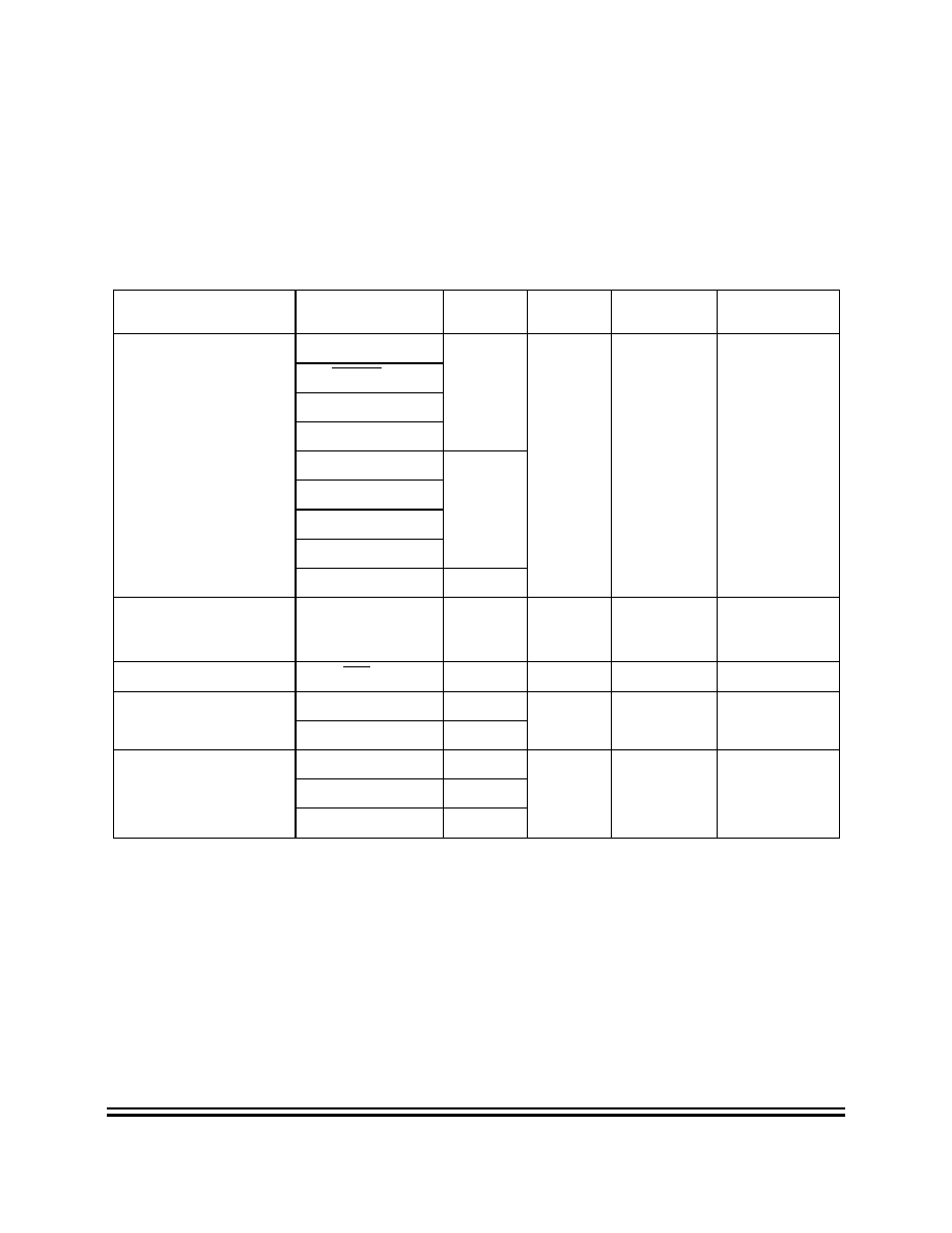
Interrupts
CPU Interrupt Processing
MC68HC(8)05PV8/A -- Rev. 1.9
Technical Data
Interrupts
NO
NDI
S
CLO
S
URE AG
REEMENT
REQ
U
IRED
When an interrupt is to be processed, the CPU fetches the address of
the appropriate interrupt software service routine from the vector table at
locations $3FF0 through $3FFF as defined in
Table 4-1
.
Table 4-1 Reset/Interrupt Vector Addresses
Function
Source
Local
Mask
Global
Mask
Priority
(1 = Highest)
Vector
Address
Reset
Power-On Logic
None
None
1
$3FFE�$3FFF
RESET Pin
COP Watchdog
Low Voltage
High Voltage
Mask
Options
High Temperature
Clock Monitor
Illegal STOP Inst.
Illegal Address
None
Software Interrupt (SWI)
User Code
None
None
Same Priority
As
Instruction
$3FFC�$3FFD
External Interrupt
IRQ Pin
INTE Bit
I-Bit
2
$3FFA�$3FFB
Core Timer Interrupts
RTIF
RTIE Bit
I-Bit
3
$3FF8�$3FF9
TOF
TOFE Bit
16-Bit Timer Interrupts
ICF Bits
ICIE Bits
I-Bit
4
$3FF6�$3FF7
OCF Bits
OCIE Bits
TOF Bit
TOIE Bit
Freescale
Semiconductor,
I
Freescale Semiconductor, Inc.
For More Information On This Product,
Go to: www.freescale.com
nc.
..

Technical Data
Technical Data
MC68HC(8)05PV8/A -- Rev. 1.9
Interrupts
NO
NDISCLOSURE AGREEMENT REQUIRED
The M68HC05 CPU does not support interruptible instructions,
therefore, the maximum latency to the first instruction of the interrupt
service routine must include the longest instruction execution time plus
stacking overhead.
Latency = (Longest instruction execution time + 10) x t
CYC
An RTI instruction is used to signify when the interrupt software service
routine is completed. The RTI instruction causes the register contents to
be recovered from the stack and normal processing to resume at the
next instruction that was to be executed when the interrupt took place.
Figure 4-1
shows the sequence of events that occur during interrupt
processing.
Voltage, Temperature
and Port C Short circuit
Interrupts
HTI Bit
HTIM Bit
I-Bit
5
$3FF4�$3FF5
HVI Bit
HVIM Bit
LVI Bit
LVIM Bit
SCIF6
SCIE6
SCIF5
SCIE5
Port A High Nibble
Interrupt
Port A4�7
PAHIE Bit
I-Bit
6
$3FF2�$3FF3
Port A Low Nibble
Interrupt
Port A0�3
PALIE Bit
Port C Contact Sense/HV
Inputs
CSIF
CSIE
I-Bit
7
$3FF0�$3FF1
Table 4-1 Reset/Interrupt Vector Addresses
Function
Source
Local
Mask
Global
Mask
Priority
(1 = Highest)
Vector
Address
Freescale
Semiconductor,
I
Freescale Semiconductor, Inc.
For More Information On This Product,
Go to: www.freescale.com
nc.
..

Interrupts
CPU Interrupt Processing
MC68HC(8)05PV8/A -- Rev. 1.9
Technical Data
Interrupts
NO
NDI
S
CLO
S
URE AG
REEMENT
REQ
U
IRED
Figure 4-1 Interrupt Processing Flowchart
Y
Y
N
FROM
RESET
I-BIT
IN CCR
SET?
CLEAR IRQ
REQUEST
LATCH
EXECUTE
INSTRUCTION
RESTORE REGISTERS
FROM STACK:
CCR,A,X,PC
STACK
PC,X,A,CCR
IRQ?
Y
N
INTERNAL
8 BIT CORE TIMER
INTERRUPT?
Y
N
INTERNAL
16 BIT TIMER
INTERRUPT?
Y
N
HIGH TEMP
LOW/HIGH VOLT, SC
INTERRUPT?
Y
N
PORT A
WIRED OR
INTERRUPT?
Y
N
PORT C0�4
CONTACT SENSE
INTERRUPT?
FETCH NEXT INSTRUCTION
Y
SWI
INSTRUCTION
?
Y
N
RTI
INSTRUCTION
?
N
SET I-BIT IN
CC REGISTER
Load PC from:
SWI:
$3FFC � $3FFD
IRQ:
$3FFA � $3FFB
Core Timer:
$3FF8 � $3FF9
16-Bit Timer:
$3FF6 � $3FF7
T, V, SC:
$3FF4 � $3FF5
PTA:
$3FF2 � $3FF3
Contact Sense: $3FF0 � $3FF1
N
Freescale
Semiconductor,
I
Freescale Semiconductor, Inc.
For More Information On This Product,
Go to: www.freescale.com
nc.
..

Technical Data
Technical Data
MC68HC(8)05PV8/A -- Rev. 1.9
Interrupts
NO
NDISCLOSURE AGREEMENT REQUIRED
4.4 Reset Interrupt Sequence
The reset function is not in the strictest sense an interrupt; however, it is
acted upon in a similar manner as shown in
Figure 4-1
. A low level input
on the RESET pin or internally generated RST signal causes the
program to vector to its starting address which is specified by the
contents of memory locations $3FFE and $3FFF. The I-bit in the
condition code register is also set. The MCU is configured to a known
state during this type of reset as described in
Section 5. Resets
.
4.5 Software Interrupt (SWI)
The SWI is an executable instruction and a non-maskable interrupt since
it is executed regardless of the state of the I-bit in the CCR. If the I-bit is
zero (interrupts enabled), the SWI instruction executes after interrupts
which were pending before the SWI was fetched, or before interrupts
generated after the SWI was fetched. The interrupt service routine
address is specified by the contents of memory locations $3FFC and
$3FFD.
4.6 Hardware Interrupts
All hardware interrupts except RESET are maskable by the I-bit in the
CCR. If the I-bit is set, all hardware interrupts (internal and external) are
disabled. Clearing the I-bit enables the hardware interrupts. There are
two types of hardware interrupts which are explained in the following
sections.
4.7 External Interrupt (IRQ)
If the interrupt mask bit (I-bit) of the CCR has been cleared and the
interrupt enable bit is set (INTE bit) and the signal of the external
interrupt pin (IRQ) satisfies the condition selected by the option control
bits (INTP and INTN), then the external interrupt is recognized. INTE,
INTP and INTN are all bits contained in the system control register
located at $000A. When the interrupt is recognized, the current state of
Freescale
Semiconductor,
I
Freescale Semiconductor, Inc.
For More Information On This Product,
Go to: www.freescale.com
nc.
..

Interrupts
External Interrupt (IRQ)
MC68HC(8)05PV8/A -- Rev. 1.9
Technical Data
Interrupts
NO
NDI
S
CLO
S
URE AG
REEMENT
REQ
U
IRED
the CPU is pushed onto the stack and the I-bit is set. This masks further
interrupts until the present one is serviced. The interrupt service routine
address is specified by the contents of memory locations $3FFA and
$3FFB.
INTP, INTN � External interrupt sensitivity options
These two bits allow the user to select which edge of the IRQ pin is
sensitive as shown in
Table 4-1
. Both bits can be written only while
the I-bit is set, and are cleared by power-on or external reset.
Therefore the device is initialized with negative edge and low level
sensitivity.
INTE � External interrupt enable
1 = External interrupt function (IRQ) enabled.
0 = External interrupt function (IRQ) disabled.
The INTE bit can be written to only while the I-bit is set, and is set by
power-on or external reset, thus enabling the external interrupt function.
$000A
Bit 7
6
5
4
3
2
1
Bit 0
Read:
POR
INTP
INTN
INTE
WCOP
WCP
FPIE
FPICLK
Write:
Reset:
NA
0
0
0
0
0
0
0
Figure 4-2 System Control Register (SYSCTRL)
Table 4-2 IRQ sensitivity
INTP
INTN
IRQ sensitivity
0
0
Negative edge and low level
sensitive
0
1
Negative edge only
1
0
Positive edge only
1
1
Positive and negative edge
sensitive
Freescale
Semiconductor,
I
Freescale Semiconductor, Inc.
For More Information On This Product,
Go to: www.freescale.com
nc.
..

Technical Data
Technical Data
MC68HC(8)05PV8/A -- Rev. 1.9
Interrupts
NO
NDISCLOSURE AGREEMENT REQUIRED
Table 4-1
describes the various triggering options available for the IRQ
pin, however it is important to re-emphasize here that in order to avoid
any conflict and spurious interrupt, it is only possible to change the
external interrupt options while the I-bit is set. Any attempt to change the
external interrupt option while the I-bit is clear will be unsuccessful. If an
external interrupt is pending, it will automatically be cleared when
selecting a different interrupt option.
NOTE:
If the external interrupt function is disabled by the INTE bit and an
external interrupt is sensed by the edge detection circuitry, then the
interrupt request is latched and the interrupt stays pending until the INTE
bit is set. The external latch of the external interrupt is cleared in the first
part of the service routine (except for the low level interrupt which is not
latched); therefore only one external interrupt pulse can be latched
during t
ILIL
and serviced as soon as the I-bit is cleared.
4.8 8-Bit Timer Interrupt
This timer can create two types of interrupts. A timer overflow interrupt
occurs whenever the 8 bit timer rolls over from $FF to $00 and the
enable bit TOFE is set. A real time interrupt occurs whenever the
programmed time elapses and the enable bit RTIE is set. This interrupt
vector to the interrupt service routine located at the address specified by
the contents of memory location $3FF8 and $3FF9.
For details see
Section 8. Core Timer
.
4.8.1 16-Bit Timer Interrupt
There are five different timer interrupt flags that cause a 16-bit timer
interrupt whenever they are set and enabled. The interrupt flags are in
the timer status register (TSR), and the enable bits are in the timer
control register1 (TCR1). Any of these interrupts vectors to the same
interrupt service routine, located at the address specified by the contents
of memory location $3FF6 and $3FF7.
For details see
Section 9. 16-Bit Programmable Timer
.
Freescale
Semiconductor,
I
Freescale Semiconductor, Inc.
For More Information On This Product,
Go to: www.freescale.com
nc.
..

Interrupts
Ambient Exception Interrupts
MC68HC(8)05PV8/A -- Rev. 1.9
Technical Data
Interrupts
NO
NDI
S
CLO
S
URE AG
REEMENT
REQ
U
IRED
4.9 Ambient Exception Interrupts
There are three different interrupt flags that cause an environmental
exception interrupt whenever they are set and enabled. The interrupt
flags are in the reset/interrupt status register (INTSR), and the enable
bits are in the interrupt control register (INTCR). Any of these interrupts
vectors to the same interrupt service routine, located at the address
specified by the contents of memory location $3FF4 and $3FF5.
4.10 High Temperature Interrupt
HTIF � High Temperature Interrupt Flag
This bit is set if the die temperature is higher than the upper trip point
and cleared again if the die temperature falls below the lower trip point
of the HTI.
1 = The die temperature is higher than T
HTION
0 = The die temperature is lower than T
HTIOFF
$0028
Bit 7
6
5
4
3
2
1
Bit 0
Read:
ULPM
0
0
0
0
HTIE
HVIE
LVIE
Write:
Reset:
0
0
0
0
0
0
0
0
Figure 4-3 Interrupt Control Register (INTCR)
$0029
Bit 7
6
5
4
3
2
1
Bit 0
Read:
RCON
PC4CL
0
0
0
HTIF
HVIF
LVIF
Write:
Reset:
NA
0
0
0
0
?
0
0
Figure 4-4 Interrupt Status Register (INTSR)
Freescale
Semiconductor,
I
Freescale Semiconductor, Inc.
For More Information On This Product,
Go to: www.freescale.com
nc.
..

Technical Data
Technical Data
MC68HC(8)05PV8/A -- Rev. 1.9
Interrupts
NO
NDISCLOSURE AGREEMENT REQUIRED
HTIE � High Temperature Interrupt Enable
This bit enables/disables the high temperature interrupt. Once this
interrupt is acknowledged, the enable bit should be cleared and the
high temperature interrupt flag should be monitored until the bit is
cleared.
1 = High temperature interrupt enabled
0 = High temperature interrupt disabled
4.10.1 High Voltage Interrupt
HVIF � High Voltage Interrupt Flag
This bit is set if the supply voltage V
SUP
is higher than the upper trip
point and cleared again if the voltage falls below the lower trip point of
the HVI.
1 = The supply voltage is higher than V
HVION
0 = The supply voltage is lower than V
HIOFF
HVIE � High Voltage Interrupt Enable
This bit enables/disables the high voltage interrupt. Once this
interrupt is acknowledged, the enable bit should be cleared and the
high voltage interrupt flag should be monitored until the bit is cleared.
1 = High voltage interrupt enabled
0 = High voltage interrupt disabled
4.10.2 Low Voltage Interrupt
LVIF � Low Voltage Interrupt Flag
This bit is set if the supply voltage V
SUP
is lower than the lower trip point
and cleared again if the voltage rises above the upper trip point of the
LVI.
1 = The supply voltage is lower than V
LVION
0 = The supply voltage is higher than V
LVIOFF
Freescale
Semiconductor,
I
Freescale Semiconductor, Inc.
For More Information On This Product,
Go to: www.freescale.com
nc.
..

Interrupts
Keyboard Interrupts
MC68HC(8)05PV8/A -- Rev. 1.9
Technical Data
Interrupts
NO
NDI
S
CLO
S
URE AG
REEMENT
REQ
U
IRED
LVIE � Low Voltage Interrupt Enable
This bit enables/disables the low voltage interrupt. Once this interrupt
is acknowledged, the enable bit should be cleared and the low voltage
interrupt flag should be monitored until the bit is cleared.
1 = Low voltage interrupt enabled
0 = Low voltage interrupt disabled
4.10.3 Power Driver Short Circuit Interrupt
There are two different interrupt flags that cause a power driver short
circuit interrupt whenever they are set and enabled. The interrupt flags
are located in the port C status register, and the enable bits are located
in the port C configuration register 1. Any of these interrupts vector to the
same interrupt service routine, located at the address specified by the
contents of memory location $3FF4 and $3FF5.
For details see
7.6 Port C (High Voltage Port)
.
4.11 Keyboard Interrupts
When configured as input pins, PA0�7 provide a wired-OR keyboard
interrupt facility and generate an interrupt provided the interrupt enable
bits (PALIE or PAHIE) in the port A configuration register are set.
The interrupt vector for this interrupt is located at $3FF2 and $3FF3.
Further information on the keyboard interrupt facility can be found in
7.4
Port A
.
4.12 Port C Contact Sense Interrupt
There is an interrupt flag that causes a contact sense interrupt whenever
it is set and enabled. This interrupt flag is a wired-OR of the active
contact sense inputs. The interrupt flag is located in the port C status
register, and the enable bit is located in the port C configuration register
1. This interrupt vectors to the memory location $3FF0 and $3FF1.
Whenever a PCxCS bit is set, but the corresponding pin is not configured
Freescale
Semiconductor,
I
Freescale Semiconductor, Inc.
For More Information On This Product,
Go to: www.freescale.com
nc.
..

Technical Data
Technical Data
MC68HC(8)05PV8/A -- Rev. 1.9
Interrupts
NO
NDISCLOSURE AGREEMENT REQUIRED
as an output, the signal for the corresponding CSDx bit, and therefore for
the contact sense interrupt, is derived from the high-voltage input circuit.
For details see
7.6 Port C (High Voltage Port)
.
4.13 STOP and WAIT Modes
All modules that are capable of generating interrupts in STOP or WAIT
mode can only do so when configured properly. The I-bit is automatically
cleared when STOP or WAIT mode is entered. Environmental exception
interrupts and interrupts detected on port A and port C are recognized in
STOP or WAIT modes.
On 68HC05PV8A, when ultra low power mode is selected by setting the
ULPM bit, there will be no LVI, HVI, HTI even if all conditions for an
asserted interrupt are beeing met.
Freescale
Semiconductor,
I
Freescale Semiconductor, Inc.
For More Information On This Product,
Go to: www.freescale.com
nc.
..

MC68HC(8)05PV8/A -- Rev. 1.9
Technical Data
Resets
NO
NDI
S
CLO
S
URE AG
REEMENT
REQ
U
IRED
Technical Data -- MC68HC(8)05PV8/A
Section 5. Resets
5.1 Contents
5.2
Introduction . . . . . . . . . . . . . . . . . . . . . . . . . . . . . . . . . . . . . . . . 77
5.3
Reset status register (RSR) . . . . . . . . . . . . . . . . . . . . . . . . . . .78
5.4
External Reset (RESET). . . . . . . . . . . . . . . . . . . . . . . . . . . . . .79
5.5
Internal Resets . . . . . . . . . . . . . . . . . . . . . . . . . . . . . . . . . . . . . 80
5.6
Power-On Reset (POR) . . . . . . . . . . . . . . . . . . . . . . . . . . . . . . 80
5.7
Computer Operating Properly Reset (COPR). . . . . . . . . . . . . . 82
5.8
Illegal Address Reset . . . . . . . . . . . . . . . . . . . . . . . . . . . . . . . . 84
5.9
Disabled STOP Instruction Reset . . . . . . . . . . . . . . . . . . . . . . .84
5.10
High Temperature Reset . . . . . . . . . . . . . . . . . . . . . . . . . . . . . 84
5.11
High Voltage Reset. . . . . . . . . . . . . . . . . . . . . . . . . . . . . . . . . . 85
5.12
Low Voltage Reset . . . . . . . . . . . . . . . . . . . . . . . . . . . . . . . . . .85
5.13
Operation in STOP and WAIT Mode . . . . . . . . . . . . . . . . . . . .85
5.14
Clock Monitor Reset (CMR) . . . . . . . . . . . . . . . . . . . . . . . . . . .85
5.14.1
Clock Monitor in STOP mode . . . . . . . . . . . . . . . . . . . . . . . 86
5.2 Introduction
The MCU can be reset from nine sources: one external input and eight
internal restart conditions. The RESET pin is an input with a Schmitt
trigger. All the internal peripheral modules are reset by the internal reset
signal (RST). Refer to
Figure 5-2
for reset timing details.
Freescale
Semiconductor,
I
Freescale Semiconductor, Inc.
For More Information On This Product,
Go to: www.freescale.com
nc.
..

Technical Data
Technical Data
MC68HC(8)05PV8/A -- Rev. 1.9
Resets
NO
NDISCLOSURE AGREEMENT REQUIRED
5.3 Reset status register (RSR)
This register contains eight flags that show the source of the last reset.
A power-on reset sets the POR bit in the system control register and
clears all other bits in the reset status register. All bits can be cleared by
writing a one to the corresponding bit. Uncleared bits remain set as long
as they are not cleared by a power-on reset or by software.
PINR � External Reset Bit
1 = Last reset caused by external reset pin (RESET)
0 = No pin reset since PINR was cleared by software or POR
STOPR � Illegal STOP Instruction Reset Bit
Indicates the last reset was caused by a disabled STOP instruction.
1 = Last reset caused by a disabled STOP instruction
0 = No illegal STOP instruction since STOPR was cleared by
software or POR
COPR � COP (Computer Operating Properly) Reset Bit
1 = Last reset caused by COP
0 = No COP reset since COPR was cleared by software or POR
ILINR � Illegal Instruction Reset Bit
1 = Last reset caused by an instruction fetch from an illegal address
0 = No illegal instruction fetch reset since ILINR was cleared by
software or POR
CMR � Clock Monitor Reset Bit
1 = Last reset caused by the clock monitor due to a failure on
system clock or system clock is back. Refer to RCON status bit
in the interrupt status register
0 = No clock monitor reset since CMR was cleared by software or
POR
$002A
Bit 7
6
5
4
3
2
1
Bit 0
Read:
PINR
STOPR
COPR
ILINR
CMR
HTR
HVR
LVR
Write:
POR:
0
0
0
0
0
0
0
0
Figure 5-1 Reset Status Register (RSR)
Freescale
Semiconductor,
I
Freescale Semiconductor, Inc.
For More Information On This Product,
Go to: www.freescale.com
nc.
..

Resets
External Reset (RESET)
MC68HC(8)05PV8/A -- Rev. 1.9
Technical Data
Resets
NO
NDI
S
CLO
S
URE AG
REEMENT
REQ
U
IRED
HTR � High Temperature Reset Bit
1 = Last reset caused by high temperature detect circuitry
0 = No high temperature reset since HTR was cleared by software
or POR
HVR � High Voltage Reset Bit
1 = Last reset caused by high voltage detect circuitry
0 = No high voltage reset since HVR is cleared by software or POR
LVR � Low Voltage Reset Bit
1 = Last reset caused by low voltage detect circuitry
0 = No low voltage reset since LVR was cleared by software or
POR
Note: If the cause of an environmental reset only lasts for a short time and if there is an external
capacitor on the RESET pin, the corresponding bit in the reset status register may be set without
occurrence of a reset.
5.4 External Reset (RESET)
The RESET pin is the only external source of a reset. This pin is
connected to a Schmitt trigger input gate to provide an upper and lower
threshold voltage separated by a minimum amount of hysteresis. This
external reset occurs whenever the RESET pin is pulled below the lower
threshold and remains in reset until the RESET pin rises above the upper
threshold. This active low input generates the RST signal and resets the
CPU and peripherals.
Activation of the RST signal is generally referred to as reset of the
device, unless otherwise specified.
The RESET pin can also act as an open drain output. It is pulled to a low
state by an internal pull-down that is activated by any reset source. This
RESET pull-down device is asserted until the internal reset source is
deasserted and the reset is internally recognized.
Freescale
Semiconductor,
I
Freescale Semiconductor, Inc.
For More Information On This Product,
Go to: www.freescale.com
nc.
..

Technical Data
Technical Data
MC68HC(8)05PV8/A -- Rev. 1.9
Resets
NO
NDISCLOSURE AGREEMENT REQUIRED
5.5 Internal Resets
The eight internally generated resets are the initial power-on reset
function, the COP watchdog timer reset, the illegal address detector,
clock-monitor, the high temperature reset, high voltage reset,
low-voltage reset, and the disabled STOP instruction.
When forcing RESET externally to V
DD
, all temperature, voltage and
clock-monitor dependent reset sources are disabled. In this case, the
internal pull-down device tries to pull down the pin until the next
recognized internal reset, which leads to some power-consumption.
5.6 Power-On Reset (POR)
The internal POR is generated on power-up to allow the clock oscillator
to stabilize. The POR is strictly for power turn-on conditions and is not
able to detect a drop in the power supply voltage (brown-out). There is
an oscillator stabilization delay of t
PORL
after the oscillator becomes
active. See
Figure 5-2
for details. T
PORL
is 4064 internal processor clock
cycles.
The POR generates the RST signal which resets the CPU. If any other
reset function is active at the end of this t
PORL
delay, the RST signal
remains in the reset condition until the other reset condition(s) ends.
POR activates the RESET pin pull-down device connected to the pin.
VDD must drop below V
POR
in order for the internal POR circuit to detect
the next rise of V
DD
.
INTERNAL
RESETS
RESET
PIN
VDD
INTERNAL
RESET
LOGIC
INTERNAL
PULLUP
Freescale
Semiconductor,
I
Freescale Semiconductor, Inc.
For More Information On This Product,
Go to: www.freescale.com
nc.
..

Resets
Power-On Reset (POR)
MC68HC(8)05PV8/A -- Rev. 1.9
Technical Data
Resets
NO
NDI
S
CLO
S
URE AG
REEMENT
REQ
U
IRED
Figure 5-2 RESET and POR Timing Diagram
PC
H
P
CL
OS
C1
2
RE
SE
T
INT
E
R
NA
L
AD
DR
ESS
BU
S
1
3F
FE
3F
FF
V
DD
t po
r
l
t cy
c
t RL
INT
E
R
NA
L
DA
TA
BU
S
1
3F
FE
3
FFE
3F
FE
3FF
E
N
EW
PC
3F
FF
NOTE
S
:
1.
I
n
t
e
rn
al
t
i
m
i
n
g
signal
and bus
inf
o
rmat
i
on not
availabl
e
ext
e
rnally.
2.
O
S
C
1
line is
not
m
eant
t
o
repres
ent
f
r
equency.
I
t
is
only us
ed t
o
r
epresent
t
i
me.
3.
T
he
n
e
xt
rising edge
of
t
he i
n
t
e
rnal proces
sor clock f
o
l
l
owing t
he rising edge
of
RE
SE
T
init
iat
e
s
t
he reset
s
equence.
4.
V
DD
m
u
st
f
a
l
l
t
o
a
leve
l
lower t
han V
PO
R
in order t
o
be
re
cognized as a
power
on reset
.
3
NE
W
NE
W
OP
CO
DE
PCL
PC
H
NE
W P
C
N
EW
PC
OP
CO
DE
NEW
P
C
0v
V
DD
> V
POR
4
IN
T
E
R
NA
L
PR
OC
ES
SO
R
CL
OC
K
1
Freescale
Semiconductor,
I
Freescale Semiconductor, Inc.
For More Information On This Product,
Go to: www.freescale.com
nc.
..

Technical Data
Technical Data
MC68HC(8)05PV8/A -- Rev. 1.9
Resets
NO
NDISCLOSURE AGREEMENT REQUIRED
5.7 Computer Operating Properly Reset (COPR)
The MCU contains a watchdog timer that automatically times out if not
reset (cleared) within a specific time by a program reset sequence. If the
COP watchdog timer is allowed to time-out, an internal reset is
generated to reset the MCU. Regardless of an internal or external reset,
the MCU comes out of a COP reset according to the pin conditions that
determine mode selection.
The COP reset function is enabled or disabled by the MOR[COPE] bit
and is verified during production testing.
The COP watchdog reset activates the internal pull-down device
connected to the RESET pin.
The window COP function can be enabled via the WCOP bit in the
system control register. This bit is a write once bit, e.g. the WCOP
feature stays enabled until the next system reset. In case of WCOP bit
enabled, the COP timer is only reset when the write to the COPEN bit in
the mask option register occurs in the second half of the COP watchdog
time. A write in the first half causes a system reset with the COPR bit set.
The phase of the COP timer can be monitored via the WCP (window
COP phase) in the system control register. A 0 indicates that writing to
the MOR bit causes system reset. A 1 indicates that writing to the MOR
bit causes a reset of the COP timer cycle.
5.7.1 Resetting the COP
A COP reset is prevented by writing a 0 to the COPR bit. This action
resets the counter and begin the time-out period again. The COPR bit is
bit 0 of address $3FF0. A read of address $3FF0 returns user data
programmed at that location.
5.7.2 COP During WAIT Mode
The COP continues to operate normally during WAIT mode. The system
should be configured to pull the device out of WAIT mode periodically
and reset the COP by writing to the COPR bit to prevent a COP reset.
Freescale
Semiconductor,
I
Freescale Semiconductor, Inc.
For More Information On This Product,
Go to: www.freescale.com
nc.
..

Resets
Computer Operating Properly Reset (COPR)
MC68HC(8)05PV8/A -- Rev. 1.9
Technical Data
Resets
NO
NDI
S
CLO
S
URE AG
REEMENT
REQ
U
IRED
5.7.3 COP During STOP Mode
When the STOP enable mask option is selected, STOP mode disables
the oscillator circuit and thereby turns the clock off for the entire device.
The COP counter is reset when STOP mode is entered. If a reset is used
to exit STOP mode, the COP counter is held in reset during the 4064
cycles of start up delay. If any operable interrupt is used to exit STOP
mode, the COP counter is not reset during the 4064 cycle start-up delay
and has the number of cycles already counted when control is returned
to the program.
5.7.4 COP Watchdog Timer Considerations
The COP watchdog timer is active in user mode if enabled by the
COPEN bit in the mask option register. If the COP watchdog timer is
selected, any execution of the STOP instruction (either intentional or
inadvertent due to the CPU being disturbed) causes the oscillator to halt
and prevent the COP watchdog timer from timing out. Therefore, it is
recommended that the STOP instruction should be disabled if the COP
watchdog timer is enabled.
If the COP watchdog timer is selected, the COP resets the MCU when it
times out. Therefore, it is recommended that the COP watchdog be
disabled for a system that must use the WAIT mode for periods longer
than the COP time-out period.
5.7.5 COP Register
The COP register is shared with the MSB of the contact sense interrupt
vector as shown in
Figure 5-3
. Reading this location returns whatever
user data has been programmed at this location. Writing a 0 to the
COPR bit in this location clears the COP watchdog timer.
Freescale
Semiconductor,
I
Freescale Semiconductor, Inc.
For More Information On This Product,
Go to: www.freescale.com
nc.
..

Technical Data
Technical Data
MC68HC(8)05PV8/A -- Rev. 1.9
Resets
NO
NDISCLOSURE AGREEMENT REQUIRED
5.8 Illegal Address Reset
An illegal address reset is generated when the CPU attempts to fetch an
instruction from either unimplemented address space ($0100 to $017F,
$0200 to $1FFF) monitor ROM ($3F00 to $3FEF) or I/O address space
($0000 to $003F).
The illegal address reset activates the internal pull-down device
connected to the RESET pin.
5.9 Disabled STOP Instruction Reset
When the mask option is selected to disable the STOP instruction,
execution of a STOP instruction results in an internal reset. This
activates the internal pull-down device connected to the RESET pin.
5.10 High Temperature Reset
The internal high temperature (HTR) reset is generated when the die
temperature rises above the high temperature threshold T
HTON
. This
condition remains active until the temperature falls below the threshold
T
HTOFF
.
This reset can be disabled by using a mask option.
$3FF0
Bit 7
6
5
4
3
2
1
Bit 0
Read:
Write:
COPR
Reset:
Figure 5-3 COP Watchdog Timer Location Register (COPR)
Freescale
Semiconductor,
I
Freescale Semiconductor, Inc.
For More Information On This Product,
Go to: www.freescale.com
nc.
..

Resets
High Voltage Reset
MC68HC(8)05PV8/A -- Rev. 1.9
Technical Data
Resets
NO
NDI
S
CLO
S
URE AG
REEMENT
REQ
U
IRED
5.11 High Voltage Reset
The internal high voltage (HVR) reset is generated when the supply
voltage V
SUP
rises above the high voltage reset threshold V
HVRON
. This
condition remains active until the supply voltage falls below the threshold
V
HVROFF
.
This reset can be disabled by using a mask option.
5.12 Low Voltage Reset
The internal low voltage (LVR) reset is generated when the supply
voltage V
DD
falls below the low voltage threshold V
LVRON
. This condition
remains active until the voltage rises above the threshold V
LVROFF
or a
proper power-on sequence occurs.
5.13 Operation in STOP and WAIT Mode
If enabled, all reset sources remain active during STOP and WAIT. Any
reset source can bring the MCU out of STOP or WAIT modes.
Since no instructions are executed in WAIT or STOP mode the illegal
address reset and the stop disabled reset cannot become active in
STOP or WAIT mode.
Since the core timer is not active in STOP mode, the COP reset cannot
become active in STOP mode.
On 68HC05PV8A, generation of HVR and HTR are suppressed if the
ultra low power mode is selected by setting the ULPM bit.
5.14 Clock Monitor Reset (CMR)
The clock monitor reset is based on an internal RC time delay. If no MCU
clock edges are detected within this RC time delay, the clock monitor can
optionally generate a system reset. The system clock is then
automatically switched to an on-chip RC oscillator. The clock monitor
function is enabled via a mask option bit. Clock monitor is used as a
Freescale
Semiconductor,
I
Freescale Semiconductor, Inc.
For More Information On This Product,
Go to: www.freescale.com
nc.
..

Technical Data
Technical Data
MC68HC(8)05PV8/A -- Rev. 1.9
Resets
NO
NDISCLOSURE AGREEMENT REQUIRED
backup for the COP system. Because the COP needs a clock to function
it is disabled when the clock stops. Therefore, the clock monitor system
can detect clock failures not detected by the COP system.
Semiconductor wafer processing causes variations of the RC timeout
values between individual devices. A processor clock frequency below
10 KHz is detected as a clock monitor error. A processor clock frequency
of 400 KHz or more prevents clock monitor errors. Using the clock
monitor when the processor clock is below 400 KHz is not
recommended.
The oscillator used for deriving the system clock can be determined by
the RCON Bit in the interrupt status register.
5.14.1 Clock Monitor in STOP mode
If STOP mode is entered, the clock monitor function is frozen. If the
device is woken from STOP mode, it continues to use the same oscillator
as before entering STOP. For the STOP mode recovery time of 4064
clock cycles, the clock monitor function is also suspended. If the device
uses an external oscillator before entering STOP mode and this
oscillator breaks during STOP, the device will no longer restart.
$0029
Bit 7
6
5
4
3
2
1
Bit 0
Read:
RCON
PC4CL
0
0
0
HTIF
HVIF
LVIF
Write:
Reset:
U
0
0
0
0
0
0
0
Figure 5-4 Interrupt Status Register (INTSR)
Freescale
Semiconductor,
I
Freescale Semiconductor, Inc.
For More Information On This Product,
Go to: www.freescale.com
nc.
..

MC68HC(8)05PV8/A -- Rev. 1.9
Technical Data
Operating Modes
NO
NDI
S
CLO
S
URE AG
REEMENT
REQ
U
IRED
Technical Data -- MC68HC(8)05PV8/A
Section 6. Operating Modes
6.1 Contents
6.2
Introduction . . . . . . . . . . . . . . . . . . . . . . . . . . . . . . . . . . . . . . . . 87
6.3
User mode . . . . . . . . . . . . . . . . . . . . . . . . . . . . . . . . . . . . . . . . 88
6.4
Monitor Mode . . . . . . . . . . . . . . . . . . . . . . . . . . . . . . . . . . . . . . 88
6.5
Low Power Modes . . . . . . . . . . . . . . . . . . . . . . . . . . . . . . . . . .88
6.5.1
STOP Mode. . . . . . . . . . . . . . . . . . . . . . . . . . . . . . . . . . . . .88
6.5.1.1
Ultra Low Power Mode . . . . . . . . . . . . . . . . . . . . . . . . . . . . 83
6.5.2
STOP Recovery . . . . . . . . . . . . . . . . . . . . . . . . . . . . . . . . . 89
6.6
WAIT Mode. . . . . . . . . . . . . . . . . . . . . . . . . . . . . . . . . . . . . . . . 91
6.2 Introduction
The normal operating mode of the MC68HC(8)05PV8/A is user (or
single chip) mode. There is also a monitor mode, primarily for
programming and evaluation purposes. In addition to these modes,
there are two low power modes which may be entered and exited at will
from user mode: STOP and WAIT.
Table 6-1
shows the conditions
required to enter the modes of operation on the rising edge of RESET,
where VTST = 2 x VDD.
Table 6-1 Operating Mode Entry Conditions
IRQ
PB0
Mode
VSS to VDD
VSS to VDD
User
VTST
VDD
Monitor
Freescale
Semiconductor,
I
Freescale Semiconductor, Inc.
For More Information On This Product,
Go to: www.freescale.com
nc.
..

Technical Data
Technical Data
MC68HC(8)05PV8/A -- Rev. 1.9
Operating Modes
NO
NDISCLOSURE AGREEMENT REQUIRED
6.3 User mode
Intended mode of operation for executing user firmware.
6.4 Monitor Mode
Used for programming the on-chip Program or Data EEPROM
(68HC805PV8) and Data EEPROM (68HC05PV8) if desired.
6.5 Low Power Modes
The MC68HC(8)05PV8/A is capable of running in one of several
low-power operational modes. The WAIT and STOP instructions provide
two modes that reduce the power required for the MCU by stopping
various internal clocks and/or the on-chip oscillator. The flows of the
STOP and WAIT modes are shown in
Figure 6-2
.
6.5.1 STOP Mode
The STOP instruction places the MCU in its lowest power consumption
mode. In STOP mode, the internal oscillator is turned off, halting all
internal processing, including timer (and COP watchdog timer)
operation.
During STOP mode, the core timer interrupt flags and interrupt enable
bits of the CTCSR register are cleared by internal hardware to remove
any pending timer interrupt requests and to disable any further timer
interrupts. The timer pre-scaler is also cleared. The I bit in the CCR is
cleared to enable external interrupts. All other registers, including the
remaining bits in the CTCSR, and memory remain unaltered. All
input/output lines remain unchanged. The processor can be brought out
of the STOP mode only by an external interrupt or RESET.
The STOP instruction can be disabled by a mask option. When disabled,
the STOP instruction causes a system reset.
Freescale
Semiconductor,
I
Freescale Semiconductor, Inc.
For More Information On This Product,
Go to: www.freescale.com
nc.
..

Operating Modes
Low Power Modes
MC68HC(8)05PV8/A -- Rev. 1.9
Technical Data
Operating Modes
NO
NDI
S
CLO
S
URE AG
REEMENT
REQ
U
IRED
6.5.1.1 Ultra Low Power Mode
The Ultra Low Power Mode is only available on the 68HC05PV8A. It is
a submode to STOP mode. The ULPM bit in the Interrupt Control
Register influences the onchip analogue circuits. On setting the ULPM
bit, PC0 .. PC4 is forced to input state, PC5/6 is switched off, opamp is
debiased, downscaler, power supply and die temperature monitors are
disabled. It is mandatory to set the ULPM bit in the last instruction prior
to executing the STOP instruction and should be reset immediately after
recovering from stop to utilize the ultra low power mode. When the mcu
is stopped, the main voltage regulator is switched off and the mcu is
supplied by a standby regulator. On any interrupt or reset, the main
regulator is switched on again and the normal STOP mode recovery
procedure is started as soon as VDD has reached the low voltage reset
threshold.
6.5.2 STOP Recovery
The processor can be brought out of the STOP mode by an external
interrupt, an environmental exception interrupt, a walk-up interrupt or
RESET. See
Figure 6-1
.
Freescale
Semiconductor,
I
Freescale Semiconductor, Inc.
For More Information On This Product,
Go to: www.freescale.com
nc.
..

Technical Data
Technical Data
MC68HC(8)05PV8/A -- Rev. 1.9
Operating Modes
NO
NDISCLOSURE AGREEMENT REQUIRED
Figure 6-1 Stop Recovery Timing Diagram
3FFE
3FFE
3FFE
3FFE
3FFF
INTERNAL
ADDRESS
BUS
INTERNAL
CLOCK
IRQ
3
IRQ
2
RESET
OSC1
1
t
ILCH
4064 t
cyc
RESET OR INTERRUPT
VECTOR FETCH
(RESET SHOWN)
t
LIH
t
RL
Notes:
1.
Represents the internal gating of the OSC1 pin.
2.
IRQ pin edge-sensitive mask option or Port A pin.
3.
IRQ pin level and edge sensitive mask option.
Freescale
Semiconductor,
I
Freescale Semiconductor, Inc.
For More Information On This Product,
Go to: www.freescale.com
nc.
..

Operating Modes
WAIT Mode
MC68HC(8)05PV8/A -- Rev. 1.9
Technical Data
Operating Modes
NO
NDI
S
CLO
S
URE AG
REEMENT
REQ
U
IRED
Figure 6-2 STOP and WAIT Flowcharts
6.6 WAIT Mode
The WAIT instruction places the MCU in a low-power consumption
mode. All CPU action is suspended, but the core timer, the 16-bit timer
(controlled by TOFF bit) and the PWM will or can remain active. An
interrupt, if enabled, from the core timer or any peripheral still active in
WAIT mode causes the MCU to exit WAIT mode.
Y
Y
Y
Y
Y
N
N
N
N
STOP
WAIT
IRQ
PORT A OR C
RESET
OSCILLATOR ACTIVE
TIMER CLOCK ACTIVE
PROCESSOR CLOCKS
STOPPED
STOP OSCILLATOR
AND ALL CLOCKS
CLEAR I BIT
16B TIMER,
CORE TIMER
INTERRUPT
N
Y
HVI, LVI
RESTART
PROCESSOR
CLOCK
TURN ON
OSCILLATOR
WAIT FOR TIME
DELAY TO
STABILIZE
1. FETCH RESET
VECTOR OR
2. SERVICE
INTERRUPT
A. STACK
B. SET I BIT
C. VECTOR TO
INTERRUPT
ROUTINE
1. FETCH RESET
VECTOR OR
2. SERVICE
INTERRUPT
A. STACK
B. SET I BIT
C. VECTOR TO
INTERRUPT
ROUTINE
OR HVR OR LVR
RESET
OR HVR OR LVR
IRQ
PORT A OR C
HVI, LVI
Freescale
Semiconductor,
I
Freescale Semiconductor, Inc.
For More Information On This Product,
Go to: www.freescale.com
nc.
..

Technical Data
Technical Data
MC68HC(8)05PV8/A -- Rev. 1.9
Operating Modes
NO
NDISCLOSURE AGREEMENT REQUIRED
During WAIT mode the I bit in the CCR is cleared to enable interrupts.
All other registers, memory and input/output lines remain in their
previous state. The core timer may be enabled to allow a periodic exit
from the WAIT mode.
WAIT mode consumes more power than STOP mode.
Freescale
Semiconductor,
I
Freescale Semiconductor, Inc.
For More Information On This Product,
Go to: www.freescale.com
nc.
..

MC68HC(8)05PV8/A -- Rev. 1.9
Technical Data
Input/Output Ports
NO
NDI
S
CLO
S
URE AG
REEMENT
REQ
U
IRED
Technical Data -- MC68HC(8)05PV8/A
Section 7. Input/Output Ports
7.1 Contents
7.2
Introduction . . . . . . . . . . . . . . . . . . . . . . . . . . . . . . . . . . . . . . . . 94
7.3
General Input/Output Programming . . . . . . . . . . . . . . . . . . . . . 94
7.4
Port A . . . . . . . . . . . . . . . . . . . . . . . . . . . . . . . . . . . . . . . . . . . . 95
7.4.1
Port A Keyboard Interrupt . . . . . . . . . . . . . . . . . . . . . . . . . . 96
7.4.2
Port A Pull-up Resistors . . . . . . . . . . . . . . . . . . . . . . . . . . .96
7.4.3
Port A Voltage Reference for A/D Converter. . . . . . . . . . . . 96
7.4.4
Port A Configuration Register . . . . . . . . . . . . . . . . . . . . . . . 97
7.4.5
Port A Interrupt Status Register . . . . . . . . . . . . . . . . . . . . . 98
7.4.6
Operational Amplifier. . . . . . . . . . . . . . . . . . . . . . . . . . . . . .98
7.5
Port B . . . . . . . . . . . . . . . . . . . . . . . . . . . . . . . . . . . . . . . . . . . 100
7.5.1
Port B Timer Channels and XOR Function . . . . . . . . . . . . 100
7.5.2
Port B PWM Channel . . . . . . . . . . . . . . . . . . . . . . . . . . . . 101
7.5.3
I/O Configuration Register. . . . . . . . . . . . . . . . . . . . . . . . . 101
7.6
Port C (High Voltage Port) . . . . . . . . . . . . . . . . . . . . . . . . . . . 102
7.6.1
Port C Timer Channels . . . . . . . . . . . . . . . . . . . . . . . . . . . 103
7.6.2
Port C PWM Channel . . . . . . . . . . . . . . . . . . . . . . . . . . . . 103
7.6.3
Port C Contact Sense Circuitry . . . . . . . . . . . . . . . . . . . . . 103
7.6.4
Port C ISO9141 Interface . . . . . . . . . . . . . . . . . . . . . . . . . 106
7.6.5
Port C Low Side Driver . . . . . . . . . . . . . . . . . . . . . . . . . . . 107
7.6.6
Port C Configuration Register 0 . . . . . . . . . . . . . . . . . . . . 109
7.6.7
Port C Configuration Register 1 . . . . . . . . . . . . . . . . . . . . 113
7.6.8
Port C Status Register. . . . . . . . . . . . . . . . . . . . . . . . . . . . 114
7.6.9
MFTEST Register . . . . . . . . . . . . . . . . . . . . . . . . . . . . . . . 116
Freescale
Semiconductor,
I
Freescale Semiconductor, Inc.
For More Information On This Product,
Go to: www.freescale.com
nc.
..

Technical Data
Technical Data
MC68HC(8)05PV8/A -- Rev. 1.9
Input/Output Ports
NO
NDISCLOSURE AGREEMENT REQUIRED
7.2 Introduction
In single chip mode there are 20 lines arranged as one 8-bit I/O port (port
A), one 5-bit I/O port (port B), and one 7-bit high-voltage I/O port (port
C). The I/O ports are programmable as either inputs or outputs under
software control of the data direction registers (see
7.3 General
Input/Output Programming
).
Port A is shared with A/D channels. Ports B and C are shared with timer
and PWM channels. Port C comprises 5 lines with contact sensors and
2 lines with low side drivers.
7.3 General Input/Output Programming
Bidirectional port lines may be programmed as an input or an output
under software control. The direction of the pins is determined by the
state of the corresponding bit in the port data direction register (DDR).
Each port has an associated DDR. Any I/O port pin is configured as an
output if its corresponding DDR bit is set to a logic one. A pin is
configured as an input if its corresponding DDR bit is cleared to a logical
zero (see
Table 7-1
and
Figure 7-1
).
At power-on or reset, all DDRs are cleared, thus configuring all port pins
as inputs. Reset does not affect the state of the data bits, thus after
power-on reset their state is unknown. The data direction registers are
capable of being written to or read by the processor. During the
programmed output state, a read of the data register actually reads the
value of the output data latch and not the I/O pin.
Table 7-1 I/O Pin Functions
R/W
(1)
DDR
I/O Pin Function
0
0
The I/O pin is in input mode. Data is written into the output data latch.
0
1
Data is written into the output data latch and output to the I/O pin.
1
0
The state of the I/O pin is read.
1
1
The I/O pin is in output mode. The output data latch is read.
1. R/W is an internal signal
Freescale
Semiconductor,
I
Freescale Semiconductor, Inc.
For More Information On This Product,
Go to: www.freescale.com
nc.
..
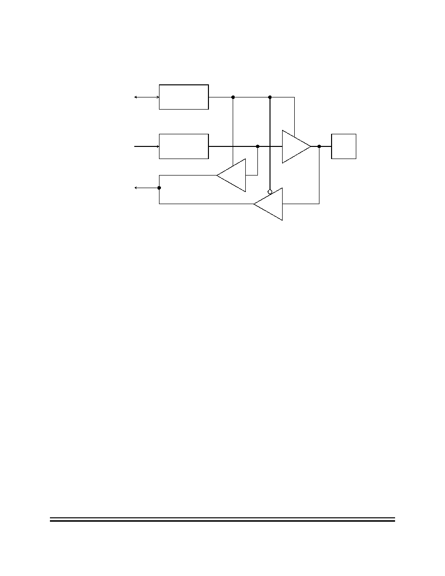
Input/Output Ports
Port A
MC68HC(8)05PV8/A -- Rev. 1.9
Technical Data
Input/Output Ports
NO
NDI
S
CLO
S
URE AG
REEMENT
REQ
U
IRED
Figure 7-1 Port I/O Circuitry
NOTE:
To avoid a glitch on the output pins, write data to the I/O port data
register before writing a one to the corresponding data direction register.
NOTE:
If the I/O pin is an input and a read-modify-write (RMW) instruction is
executed, the I/O pin will be read into the HC05 CPU and the computed
result will then be written to the data latch.
7.4 Port A
Port A is an 8-bit bidirectional port (PA0�7) with interrupt capability,
shared with the A/D converter (AN1�6, VREFL, VREFH).
The port A data register is located at $0000 and the data direction register
(DDR) at $0004. Reset does not affect the data registers, but clears the
data direction registers, thereby returning the ports to inputs. Writing a
one to a DDR bit sets the corresponding port bit to output mode.
When the A/D converter is turned on, one of the channels AN1�6 may
be selected through the A/D status and control register for conversion.
The input lines of port A include software programmable pull-up
resistors.
Data Direction
Register Bit
Latched Output
Data Bit
I/O
Pin
Input
Reg
Bit
Input
I/O
Output
Internal
HC05
Connections
Freescale
Semiconductor,
I
Freescale Semiconductor, Inc.
For More Information On This Product,
Go to: www.freescale.com
nc.
..

Technical Data
Technical Data
MC68HC(8)05PV8/A -- Rev. 1.9
Input/Output Ports
NO
NDISCLOSURE AGREEMENT REQUIRED
7.4.1 Port A Keyboard Interrupt
The keyboard interrupt consists of 8 individual edge-sensitive interrupts
with 8 interrupt flags. The keyboard interrupt is generated by a logical
OR function of the 8 interrupt flags. The interrupt inputs are connected
to PA0�7. All interrupts are maskable. If the interrupt mask bit (I bit) in
the condition code register is set, all interrupts are disabled.
The interrupts are split in two groups of four lines each (PA0�3 and
PA4�7). All interrupts of one group can be simultaneously masked by
the corresponding PAIE bits in the port A configuration register. The
trigger edges of the interrupt lines are selectable for each group with the
EDGE bits in the port A configuration register.
The port A interrupt status register indicates which interrupt request is
pending.
7.4.2 Port A Pull-up Resistors
The PA0�7 input lines have internal pull-up resistors. The port A lines
form two groups with four lines each (PA0�3 and PA4�7). All pull-up�s of
one group can be switched on with the PULEN or PUHEN bits of the port
A configuration register by resetting the bit to 0. They are disabled
�
when the enable bit is set to 1
�
when a line is configured as output.
7.4.3 Port A Voltage Reference for A/D Converter
The lines PA0 and PA7 can be connected to the reference inputs for the
A/D converter (VREFL and VREFH). In order to connect the reference
inputs, the corresponding VRHEN or VRLEN bits of the port A
configuration register have to be set. In addition, the corresponding lines
(PA0 or PA7) must be configured as inputs.
The pull-up resistor should be disabled when a line is used as A/D input
or A/D reference channel.
Freescale
Semiconductor,
I
Freescale Semiconductor, Inc.
For More Information On This Product,
Go to: www.freescale.com
nc.
..

Input/Output Ports
Port A
MC68HC(8)05PV8/A -- Rev. 1.9
Technical Data
Input/Output Ports
NO
NDI
S
CLO
S
URE AG
REEMENT
REQ
U
IRED
7.4.4 Port A Configuration Register
VRHEN � Enable A/D High Reference Channel
Those bits connect the PA7 pin with the A/D high reference channel.
1 = A/D high reference channel connected to external VREFH.
0 = A/D high reference channel connected to internal voltage
supply.
PUHEN � PA4�7 Pull-Up Resistor Enable Higher Nibble
This bit disables/enables the pull-up resistors of the PA4�7 pins.
1 = PA4�7 pull-up resistors disabled
0 = PA4�7 pull-up resistors enabled
EDGEH � PA4�7 Interrupt Edge Higher Nibble
This bit selects the trigger edges of the interrupt lines PA4�7.
1 = Rising edge sensitive
0 = Falling edge sensitive
PAHIE � PA4�7 Interrupt Enable Higher Nibble
This bit disables/enables the PA4�7 pins as an interrupt group.
1 = PA4�7 interrupt enabled
0 = PA4�7 interrupt disabled
PULEN � PA0�3 Pull-Up Resistor Enable Lower Nibble
This bits disables/enables the pull-up resistors of the PA0�3 pins.
1 = PA0�3 pull-up resistors disabled
0 = PA0�3 pull-up resistors enabled
EDGEL � PA0�3 Interrupt Edge Lower Nibble
This bit selects the trigger edges of the interrupt lines PA0�3.
1 = Rising edge sensitive
0 = Falling edge sensitive
$0020
Bit 7
6
5
4
3
2
1
Bit 0
Read:
VRHEN
PUHEN
EDGEH
PAHIE
PULEN
EDGEL
PALIE
VRLEN
Write:
Reset:
0
0
0
0
0
0
0
0
Figure 7-2 Port A Configuration Register (PACFG)
Freescale
Semiconductor,
I
Freescale Semiconductor, Inc.
For More Information On This Product,
Go to: www.freescale.com
nc.
..

Technical Data
Technical Data
MC68HC(8)05PV8/A -- Rev. 1.9
Input/Output Ports
NO
NDISCLOSURE AGREEMENT REQUIRED
PALIE � PA0�3 Interrupt Enable Lower Nibble
This bit disables/enables the PA0�3 pins as interrupt group.
1 = PA0�3 interrupt enabled
0 = PA0�3 interrupt disabled
VRLEN � Enable A/D Low Reference Channel
This bit connects the PA0 pin with the A/D low reference channel.
1 = A/D low reference channel connected to external VREFL.
0 = A/D low reference channel connected to internal ground.
7.4.5 Port A Interrupt Status Register
PAIF0�7 � Port A Interrupt Flags
These flags indicate which of the port A interrupt requests is pending.
The 8 interrupt flags can be reset individually if a 1 is written to the bit
position.
1 = Flag set when corresponding transition is sensed (if interrupt
enabled). Writing a 1 clears the flag
0 = No interrupt. Writing a 0 has no effect
7.4.6 Operational Amplifier
Pins PA4�6 are connected to an operational amplifier. The operational
amplifier is intended for amplifying small signals over VSS to increase
the resolution of the A/D converter. The output stage of this operational
amplifier is asymmetrical and thus optimized for driving loads to VSS
while keeping the quiescent current low. The output of the operational
amplifier is connected to channel 4 of the A/D converter. The amplifier is
enabled by the I/O configuration register Bit6. As long as IOCFG Bit6 is
0, the presence of the operational amplifier is without any effect. If the
opamp is enabled, first ensure that the PA4 is switched to input mode.
$0024
Bit 7
6
5
4
3
2
1
Bit 0
Read:
PAIF7
PAIF6
PAIF5
PAIF4
PAIF3
PAIF2
PAIF1
PAIF0
Write:
Reset:
0
0
0
0
0
0
0
0
Figure 7-3 Port A Interrupt Status Register (PAISR)
Freescale
Semiconductor,
I
Freescale Semiconductor, Inc.
For More Information On This Product,
Go to: www.freescale.com
nc.
..

Input/Output Ports
Port A
MC68HC(8)05PV8/A -- Rev. 1.9
Technical Data
Input/Output Ports
NO
NDI
S
CLO
S
URE AG
REEMENT
REQ
U
IRED
NOTE:
Pull-up resistors on PA4�6 should be disabled when using the
operational amplifier.
Figure 7-4 Operational Amplifier
Figure 7-5 Typical application: positive Vgain amplifier
�
Keep V
in
limited between V
SS
and V
DD
�
For precise measurements, R1 + R2 should be in the range of
50k
and the V
out
should not reach V
DD
�
External loads should be connected to ground, due to small
current sinking capability.
�
In case of V
in
x
gain
>= V
DD
(i.e. the output of the operational
amplifier cannot follow the input anymore) channel 6 (input)
should be converted to read the input voltage V
in
directly.
PA6
PA5
PA4
+
�
IOCFG Bit6
PA6
PA5
PA4
+
�
VSS
M
V
in
to A/D
Shunt
Resistor
R2
R1
a
gain
=
R2 + R1
R1
V
out
Freescale
Semiconductor,
I
Freescale Semiconductor, Inc.
For More Information On This Product,
Go to: www.freescale.com
nc.
..
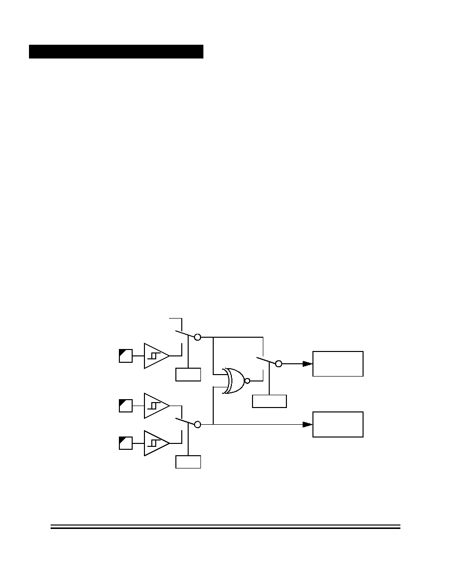
Technical Data
Technical Data
MC68HC(8)05PV8/A -- Rev. 1.9
Input/Output Ports
NO
NDISCLOSURE AGREEMENT REQUIRED
7.5 Port B
Port B is a 5-bit bidirectional port, shared with timer and PWM channels
(TCAP, TCMP, PWM). An XOR function is provided for one timer
capture channel.
The port B data register is at $0001 and the data direction register (DDR)
is at $0005. Reset does not affect the data registers, but clears the data
direction registers, thereby returning the ports to inputs. Writing a one to
a DDR bit sets the corresponding port bit to output mode.
7.5.1 Port B Timer Channels and XOR Function
The port pins PB0�PB3 are shared with the 16-bit timer channels
(TCAP1�2, TCMP1�2). The timer capture channel TCAP1 can be driven
by the XOR of two channels if TXOR bit in the I/O Configuration Register
is set (see
Figure 7-6
).TCAP1 status can be read by the CPU by polling
bit 5 of the Port B Data Register.
Figure 7-6 Mapping Ports to Timer Capture Channels
TCAP1
PB0
PB0IC
0
1
PB2
PC2
PB2IC
0
1
TXOR
0
1
Capture
Channel 1
Capture
Channel 2
FROM PC0 OR C4
Freescale
Semiconductor,
I
Freescale Semiconductor, Inc.
For More Information On This Product,
Go to: www.freescale.com
nc.
..

Input/Output Ports
Port B
MC68HC(8)05PV8/A -- Rev. 1.9
Technical Data
Input/Output Ports
NO
NDI
S
CLO
S
URE AG
REEMENT
REQ
U
IRED
7.5.2 Port B PWM Channel
The port pin PB4 is shared with the PWM channel. In order to connect
this pin to the PWM channel, the corresponding bit PWM4 of the I/O
configuration register must be set.
7.5.3 I/O Configuration Register
TXOR � Timer EXOR Enable
This bit enables the EXOR of the TCAP1 channel
1 = EXOR enabled
0 = EXOR disabled
OPAMP � Enable Operational Amplifier
This bit enables the operational amplifier on PA6
1 = Opamp enabled
0 = Opamp disabled
PB4PW � PB4 PWM Enable
This bit enables the PB4 pin as PWM output.
1 = PB4 PWM enabled. PBDD4 bit must be set in order to drive the
output
0 = PB4 PWM disabled
PB3OC � PB3 Output Compare Enable
This bit enables the PB3 pin for output compare channel 2.
1 = PB3 output compare channel 2 enabled. PBDD3 bit must be set
in order to drive the output
0 = PB3 output compare channel 2 disabled
$0021
Bit 7
6
5
4
3
2
1
Bit 0
Read:
TXOR
OPAMP
PB4PW
PB3OC
PB2IC
PB1OC
PB0IC
Write:
Reset:
0
0
0
0
0
0
0
0
Figure 7-7 I/O Configuration Register (IOCFG)
Freescale
Semiconductor,
I
Freescale Semiconductor, Inc.
For More Information On This Product,
Go to: www.freescale.com
nc.
..

Technical Data
Technical Data
MC68HC(8)05PV8/A -- Rev. 1.9
Input/Output Ports
NO
NDISCLOSURE AGREEMENT REQUIRED
PB2IC � PB2 Input Capture Enable
This bit enables the PB2 pin to drive the input capture channel 2.
1 = PB2 drives the input capture channel 2
0 = PC2 drives the input capture channel 2
PB1OC � PB1 Output Compare Enable
This bit enables the PB1 pin for output compare channel 1.
1 = PB1 output compare channel 1 enabled. PBDD1 bit must be set
in order to drive the output
0 = PB1 output compare channel 1disabled
PB0IC � PB0 Input Capture Enable
This bit enables the PB0 pin to drive the input capture channel 1.
1 = PB0 drives the input capture channel 1
0 = PC0 or PC4 drives the input capture channel 1
7.6 Port C (High Voltage Port)
Port C is a 7-bit multifunctional and bidirectional port (PC0�6) with high
voltage capability. The port is shared with timer and PWM channels
(TCAP, TCMP, PWM) and provides a special contact sense feature with
interrupt capability.
In addition, port C comprises a low ohmic two channel low side driver
with internal Zener diode turn-off for switching inductive loads.
The port C data register is at $0002 and the data direction register (DDR)
is at $0006. Reset does not affect the data registers, but clears the data
direction registers, thereby returning the PC0�4 to high voltage inputs,
PC5 and PC6 are switched to the off state. Writing a one to a DDR bit
sets the corresponding port bit to output or contact sense mode.
The port C pins PC5�6 are open drain outputs only without internal
pull-ups.
The voltage levels of PC0�4 I/O signals are related to the V
SUP
and V
SS
levels respectively. PC5�6 have an additional power supply pin for VSS
(PVSS) to which the low side drivers relate.
Freescale
Semiconductor,
I
Freescale Semiconductor, Inc.
For More Information On This Product,
Go to: www.freescale.com
nc.
..

Input/Output Ports
Port C (High Voltage Port)
MC68HC(8)05PV8/A -- Rev. 1.9
Technical Data
Input/Output Ports
NO
NDI
S
CLO
S
URE AG
REEMENT
REQ
U
IRED
7.6.1 Port C Timer Channels
The port pins PC0�5 are shared with the 16-bit timer channels
(TCAP1�2, TCMP1�2).
7.6.2 Port C PWM Channel
The port pins PC0, 4�6 are shared with the PWM channel. In order to
connect those pins, please refer to
7.6.6 Port C Configuration
Register 0
for details.
7.6.3 Port C Contact Sense Circuitry
The port C pins PC0�4 have a special contact sense circuit (see
Figure
7-8
,
Figure 7-9
,
Figure 7-10
). This feature allows, for example, the
monitoring of mechanical contacts in automotive applications (switch
monitor).
Figure 7-8 PC0 Contact Sense Circuitry
Contact
Sense
CSDT
PC0
DATA
DDR
I
PIN
CSEN&DATA&DDRC
Interrupt
R
EXT
VSUP
VSS
Freescale
Semiconductor,
I
Freescale Semiconductor, Inc.
For More Information On This Product,
Go to: www.freescale.com
nc.
..

Technical Data
Technical Data
MC68HC(8)05PV8/A -- Rev. 1.9
Input/Output Ports
NO
NDISCLOSURE AGREEMENT REQUIRED
Figure 7-9 PC1�3 Contact Sense Circuitry
Figure 7-10 PC4 Contact Sense Circuitry 68HC(8)05PV8
Contact
Sense
Contact
Sense
CSDT
PC1�3
DATA
DDR
I
PIN
CSEN&DATA&DDRC
Interrupt
R
EXT
CSEN&DATA&DDRC
VSUP
VSS
Contact
Sense
CSDT
PC4
DATA
DDR
I
PIN
Interrupt
R
EXT
CSEN&DATA&DDRC
ISOMODE
VSUP
VSS
Freescale
Semiconductor,
I
Freescale Semiconductor, Inc.
For More Information On This Product,
Go to: www.freescale.com
nc.
..

Input/Output Ports
Port C (High Voltage Port)
MC68HC(8)05PV8/A -- Rev. 1.9
Technical Data
Input/Output Ports
NO
NDI
S
CLO
S
URE AG
REEMENT
REQ
U
IRED
Figure 7-11 PC4 Circuitry 68HC05PV8A
Port pin PC0 comprises a circuit that senses the outside resistance R
PIN
to VSUP. PC4 has a different circuit, which senses the outside
resistance R
PIN
to VSS (only on 68HC(8)05PV8). PC1, PC2 and PC3
have an universal one, which senses the outside resistance either to
VSS or to VSUP, depending on the state of the corresponding data
register bit.
The contact sense circuitry is enabled by setting the corresponding bits
PC4CS, PC3CS, PC2CS, PC1CS or PC0CS of the port C configuration
register to 1. In addition, the pin has to be configured as an output by
setting the corresponding DDR bit to 1 and the data bit to 0 (for R
PIN
to
VSUP, e.g. external switch to VSUP) or to 1 (for R
PIN
to VSS, e.g.
external switch to VSS). If the outside resistance R
PIN
is lower than the
specified value, the contact sense circuitry interprets this as a logical 1.
The principal sense characteristic is given in
Figure 7-12
. The result of
this sense operation is given by the bits CSD4, CSD3, CSD2, CSD1 and
CSD0 of the port C status register.
CSDT
PC4
DATA
DDR
Interrupt
VSS
Freescale
Semiconductor,
I
Freescale Semiconductor, Inc.
For More Information On This Product,
Go to: www.freescale.com
nc.
..
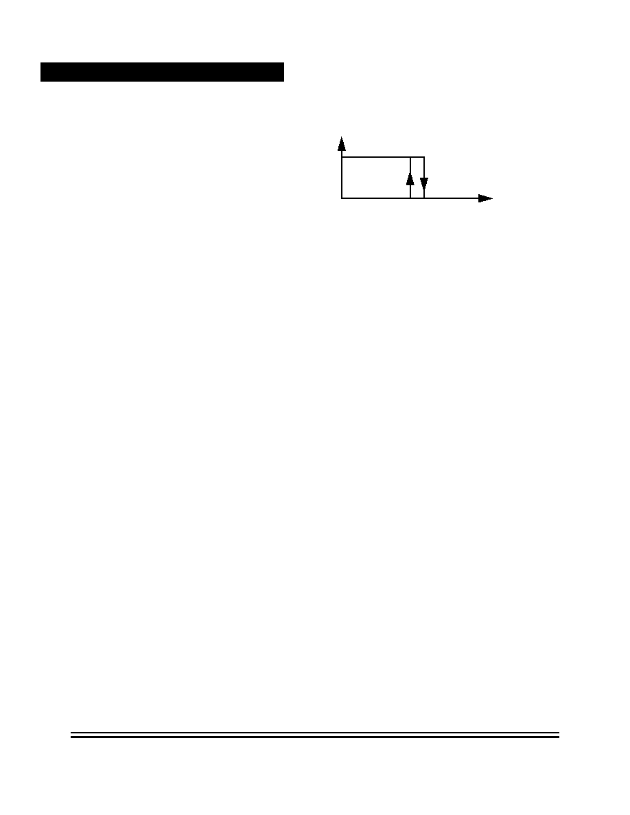
Technical Data
Technical Data
MC68HC(8)05PV8/A -- Rev. 1.9
Input/Output Ports
NO
NDISCLOSURE AGREEMENT REQUIRED
Figure 7-12 Principal Characteristic of the Contact Sense Circuitry
When setting PCXCS and clearing the corresponding DDR bit, the
signal generated by the high voltage input block is used instead of
the one of the contact sense block to drive the CSD bits. The CSD
bits will in this case reflect a logical 1 if the corresponding input
voltage is below HV
IL
, and a logical 0 if the input voltage is above
HV
IH
.
A contact sense interrupt is generated if the status of any CSD bit
changes with the corresponding PCXCS bit set. The interrupt trigger
occurs on both edges of the CSD bit change and sets the CSIF flag in
the port C status register.
The interrupt can be masked by the CSIE bit of the port C configuration
register.
An external resistor has to be placed in serial to PC0-4 because of two
reasons:
�
limit internal power dissipation,
�
internal substrate current injection may occur if the pin voltage is
out of the supply voltage range.
7.6.4 Port C ISO9141 Interface
To use Port C4 as an ISO9141 physical interface, Port C4 must be
always programmed as an output. This automatically enables the
biasing circuit for the ISO9141 driver. Furthermore, the ISOM bit in the
Port C Configuration Register 0 has to be set. This driver incorporates
an overcurrent limitation circuit. Because of excessive power dissipation
0
1
Contact Sense
Data Bit
Outside Resistance
CSD4�0
Freescale
Semiconductor,
I
Freescale Semiconductor, Inc.
For More Information On This Product,
Go to: www.freescale.com
nc.
..

Input/Output Ports
Port C (High Voltage Port)
MC68HC(8)05PV8/A -- Rev. 1.9
Technical Data
Input/Output Ports
NO
NDI
S
CLO
S
URE AG
REEMENT
REQ
U
IRED
the software should take care to switch off the driver as soon as possible
whenever a short-circuit occurs. To detect such a condition the PC4CL
(Bit 6) in the Interrupt Status Register should be polled.
Figure 7-13 Interrupt Status Register (INTSR)
MC68HC(8)05PV8 (maskset J47D and J31D):
PC4CL - Port C4 in current limit mode
1 = current on PC4 exceeds limit
0 = current on PC4 below limit
MC68HC05PV8A (maskset K20R):
PC4CL - Port C4 in current limit mode
1 = current on PC4 below limit
0 = current on PC4 exceeds limit
If the timer input capture 1 is configured to Port C4, the state of the PC4
pin is transfered to the timer module input capture, the input status can
be polled by reading the TCAP1 bit in the Port B Data Register.
7.6.5 Port C Low Side Driver
The port C pins PC5�6 comprise of two low side driver channels which
are shared with the PWM function. The channels can either be controlled
directly by the data register or are linked to the PWM function (see
7.6.2
Port C PWM Channel
).
The low side driver channels are open-drain outputs with an internal
Zener diode. The diode clamps the maximum output voltage and limits
the turn-off time of inductive loads (see
Figure 7-14
).
$0029
Bit 7
6
5
4
3
2
1
Bit 0
Read:
RCON
PC4CL
0
0
0
HTIF
HVIF
LVIF
Write:
Reset:
NA
0/1
0
0
0
?
0
0
Freescale
Semiconductor,
I
Freescale Semiconductor, Inc.
For More Information On This Product,
Go to: www.freescale.com
nc.
..
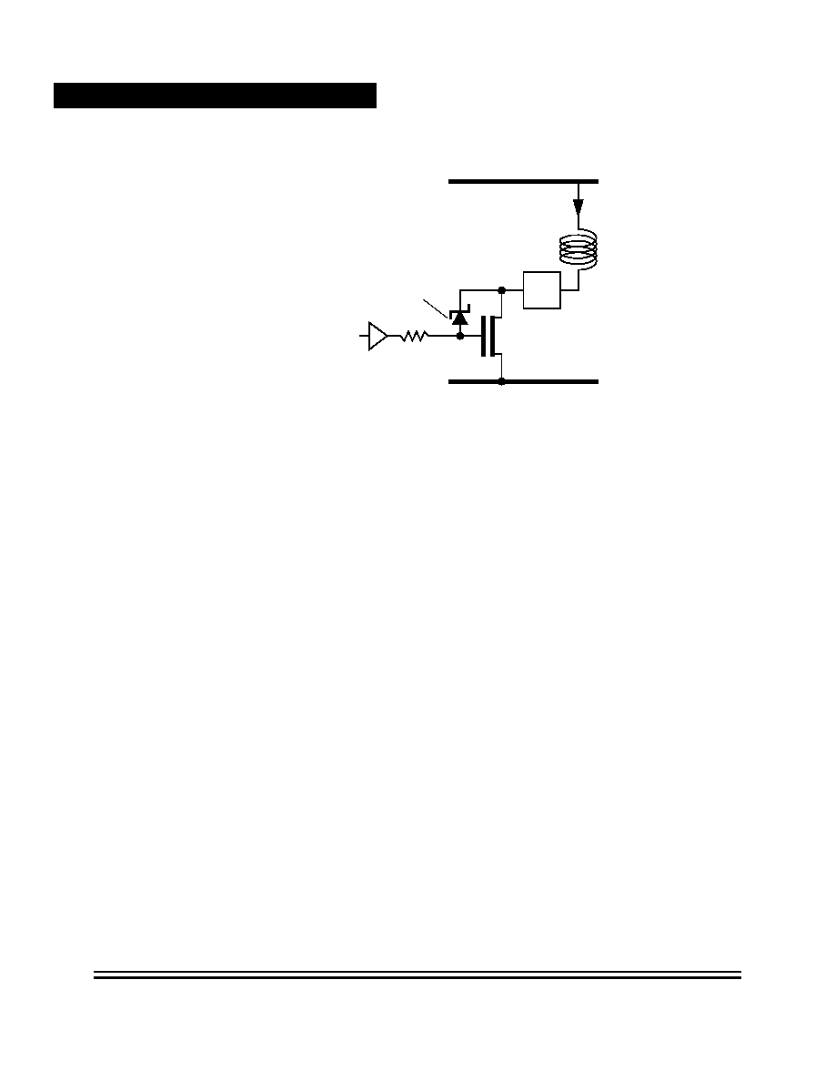
Technical Data
Technical Data
MC68HC(8)05PV8/A -- Rev. 1.9
Input/Output Ports
NO
NDISCLOSURE AGREEMENT REQUIRED
Figure 7-14 Principle of Port C Low Side Driver
A permanent external pin voltage above the minimum Zener break-down
voltage can destroy the driver.
The low side drivers have a short circuit protection feature. Whenever
the drain current of the LDMOS transistor exceeds a fixed value, the
output is automatically switched off (i.e. the LDMOS is in the high
impedance state) and the corresponding short circuit flag is set (SCIF5
or SCIF6). If the SCIE5/6 bits are enabled, an interrupt occurs. As long
as the SCIF5/6 bits are set, the output cannot be switched on. These bits
are cleared by writing a logical 1 to the corresponding bit location. The
outputs are also protected by a common over temperature detection.
See
Figure 7-15
for details.
VSUP
Fast Turn-Off
LDMOS
Solenoid
PVSS
PC5�6
Zener Diode
Freescale
Semiconductor,
I
Freescale Semiconductor, Inc.
For More Information On This Product,
Go to: www.freescale.com
nc.
..

Input/Output Ports
Port C (High Voltage Port)
MC68HC(8)05PV8/A -- Rev. 1.9
Technical Data
Input/Output Ports
NO
NDI
S
CLO
S
URE AG
REEMENT
REQ
U
IRED
Figure 7-15 Short Circuit Diagnostic of Port C Low Side Driver
7.6.6 Port C Configuration Register 0
ISOM � Driver Mode of PC4
This bit selects the driver mode of PC4. The ISOM bit is without
function on 68HC05PV8A.
1 = ISO9141 compatible output (low side driver only)
0 = PC4 is a push-pull output
PC6PW � PC6 PWM Enable
This bit enables the PC6 pin as PWM output.
1 = PC6 PWM enabled.
0 = PC6 PWM disabled
$0022
Bit 7
6
5
4
3
2
1
Bit 0
Read:
ISOM
PC6PW
PWMS1
PWMS0
PC3OC
TS2
TS1
TS0
Write:
Reset:
0
0
0
0
0
0
0
0
Figure 7-16 Port C Configuration Register 0 (PCCFG0)
PC6�5
SOUT
PORT C DATA
DRIVE CONTROL
OVERCURRENT
DETECTION
SCIF5/6
PVSS
Freescale
Semiconductor,
I
Freescale Semiconductor, Inc.
For More Information On This Product,
Go to: www.freescale.com
nc.
..
Technical Data
Technical Data
MC68HC(8)05PV8/A -- Rev. 1.9
Input/Output Ports
NO
NDISCLOSURE AGREEMENT REQUIRED
PWMS1, PWMS0 � PWM Select Bits
These bits select the output pin for the PWM on PC0, PC4 or PC5.
PC3OC � PC3 Output Compare Enable
This bit enables the PC3 pin for output compare channel 2.
1 = PC3 output compare channel 2 enabled. PC3 DDR bit must be
set in order to drive the output
0 = PC3 output compare channel 2 disabled
TS2, TS1, TS0 � Timer Channel 1 Select Bits
These bits select the input and output pins for the timer channel 1.
NOTE:
If PC0, PC1, PC4 and PC5 are neither switched to PWM nor to timer
output compare, the output states of these pins follow the states of their
data register bits.
Table 7-2 PWM Select
PWMS1
PWMS0
PWM Output at Port C
0
0
none
0
1
PC0
1
0
PC4
1
1
PC5
Table 7-3 Timer Channel 1 Select
TS2
TS1
TS0
Output Compare at PCX
Input Capture at PCX
0
0
0
none, Bit I/O
PC0
0
0
1
none, Bit I/O
PC4
0
1
0
PC0 PC0
0
1
1
PC0
PC4
1
0
0
PC1
PC0
1
0
1
PC1
PC4
1
1
0
PC4
PC4
1
1
1
PC5
PC4
Freescale
Semiconductor,
I
Freescale Semiconductor, Inc.
For More Information On This Product,
Go to: www.freescale.com
nc.
..

Input/Output Ports
Port C (High Voltage Port)
MC68HC(8)05PV8/A -- Rev. 1.9
Technical Data
Input/Output Ports
NO
NDI
S
CLO
S
URE AG
REEMENT
REQ
U
IRED
To enable either PWM or output compare function the corresponding
DDR bit must be set to 1.
If PWM and timer output compare functions are routed to the same pin,
PC0 and PC4 would be connected to the output compare signal, PC5
would be connected to the PWM signal.
For using the input capture be sure that the PB0IC bit in the I/O
configuration register is set to 0, and the corresponding pin PC0 or PC4
is switched to input mode. PC4 may also be in the ISO9141 compatible
mode.
For using the contact sense function, it is not recommended to route any
special signal to the corresponding pins.
Freescale
Semiconductor,
I
Freescale Semiconductor, Inc.
For More Information On This Product,
Go to: www.freescale.com
nc.
..

Technical Data
Technical Data
MC68HC(8)05PV8/A -- Rev. 1.9
Input/Output Ports
NO
NDISCLOSURE AGREEMENT REQUIRED
Figure 7-17 Port C Special Signal Routing
PC0
PC2
PC4
PC1
PC3
PC5
PC6
PC6PW
PWMS1,0
PWM
PC3OC
TOC2
TS2,1,0
DDRC, TS2,1,0, PWS1,0
TOC1
Port C Data 0
Port C Data 1
Port C Data 2
Port C Data 3
Port C Data 4
Port C Data 5
Port C Data 6
PB0
PB2
TS2,1,0
PB2OC
PB0OC
TXOR
TIC1
TIC2
Freescale
Semiconductor,
I
Freescale Semiconductor, Inc.
For More Information On This Product,
Go to: www.freescale.com
nc.
..

Input/Output Ports
Port C (High Voltage Port)
MC68HC(8)05PV8/A -- Rev. 1.9
Technical Data
Input/Output Ports
NO
NDI
S
CLO
S
URE AG
REEMENT
REQ
U
IRED
7.6.7 Port C Configuration Register 1
CSIE � Port C Contact Sense Interrupt Enable
This bit enables contact sense interrupt of the lines PC4�0.
1 = Port C contact sense interrupt enabled
0 = Port C contact sense interrupt disabled
SCIE6 � Low Side Driver Short Circuit Interrupt Enable
This bit enables short circuit interrupt of the low side driver PC6.
1 = Low side driver short circuit interrupt enabled
0 = Low side driver short circuit interrupt disabled
SCIE5 � Low Side Driver Short Circuit Interrupt Enable
This bit enables short circuit interrupt of the low side driver PC5.
1 = Low side driver short circuit interrupt enabled
0 = Low side driver short circuit interrupt disabled
PC4CS � PC4 Contact Sense Enable
This bit enables the PC4 contact sense circuitry.
1 = PC4 contact sense circuitry enabled
0 = PC4 contact sense circuitry disabled
PC3CS � PC3 Contact Sense Enable
This bit enables the PC3 contact sense circuitry.
1 = PC3 contact sense circuitry enabled
0 = PC3 contact sense circuitry disabled
PC2CS � PC2 Contact Sense Enable
This bit enables the PC2 contact sense circuitry.
1 = PC2 contact sense circuitry enabled
0 = PC2 contact sense circuitry disabled
$0026
Bit 7
6
5
4
3
2
1
Bit 0
Read:
CSIE
SCIE6
SCIE5
PC4CS
PC3CS
PC2CS
PC1CS
PC0CS
Write:
Reset:
0
0
0
0
0
0
0
0
Figure 7-18 Port C Configuration Register 1 (PCCFG1)
Freescale
Semiconductor,
I
Freescale Semiconductor, Inc.
For More Information On This Product,
Go to: www.freescale.com
nc.
..

Technical Data
Technical Data
MC68HC(8)05PV8/A -- Rev. 1.9
Input/Output Ports
NO
NDISCLOSURE AGREEMENT REQUIRED
PC1CS � PC1 Contact Sense Enable
This bit enables the PC1 contact sense circuitry.
1 = PC1 contact sense circuitry enabled
0 = PC1 contact sense circuitry disabled
PC0CS � PC0 Contact Sense Enable
This bit enables the PC0 contact sense circuitry.
1 = PC0 contact sense circuitry enabled
0 = PC0 contact sense circuitry disabled
7.6.8 Port C Status Register
CSIF � Port C Contact Sense Interrupt Flag
This flag indicates that a contact sense transition has occurred and an
interrupt request is pending. The flag can be cleared by writing a 1 to
it.
1 = Flag set when a transition is sensed by the contact sense
circuitry
0 = No interrupt
SCIF6 � Low Side Driver Short Circuit Interrupt Flag
This flag indicates a short circuit on PC6 is active and an interrupt
request is pending.
1 = Short circuit at the PC6 pin; PC6 is switched to high impedance
0 = No short circuit at the PC6 pin
$0027
Bit 7
6
5
4
3
2
1
Bit 0
Read:
CSIF
SCIF6
SCIF5
CSD4
CSD3
CSD2
CSD1
CSD0
Write:
Reset:
0
0
0
0
0
0
0
0
Figure 7-19 Port C Status Register (PCSTR)
Freescale
Semiconductor,
I
Freescale Semiconductor, Inc.
For More Information On This Product,
Go to: www.freescale.com
nc.
..

Input/Output Ports
Port C (High Voltage Port)
MC68HC(8)05PV8/A -- Rev. 1.9
Technical Data
Input/Output Ports
NO
NDI
S
CLO
S
URE AG
REEMENT
REQ
U
IRED
SCIF5 � Low Side Driver Short Circuit Interrupt Flag
This flag indicates a short circuit on PC5 is active and an interrupt
request is pending.
1 = Short circuit at the PC5 pin; PC5 is switched to high impedance
0 = No short circuit at the PC5 pin
CSD4 � PC4 Contact Sense Data
This data bit represents the result of the PC4 contact sense circuitry.
1 = Low resistance sensed (see
Figure 7-12
), or input PC4 is 0.
0 = High resistance sensed
CSD3 � PC3 Contact Sense Data
This data bit represents the result of the PC3 contact sense circuitry.
1 = Low resistance sensed (see
Figure 7-12
), or input PC3 is 0.
0 = High resistance sensed
CSD2 � PC2 Contact Sense Data
This data bit represents the result of the PC2 contact sense circuitry.
1 = Low resistance sensed (see
Figure 7-12
), or input PC2 is 0.
0 = High resistance sensed
CSD1 � PC1 Contact Sense Data
This data bit represents the result of the PC1 contact sense circuitry.
1 = Low resistance sensed (see
Figure 7-12
), or input PC1 is 0.
0 = High resistance sensed
CSD0 � PC0 Contact Sense Data
This data bit represents the result of the PC0 contact sense circuitry.
1 = Low resistance sensed (see
Figure 7-12
), or input PC0 is 0.
0 = High resistance sensed
Freescale
Semiconductor,
I
Freescale Semiconductor, Inc.
For More Information On This Product,
Go to: www.freescale.com
nc.
..

Technical Data
Technical Data
MC68HC(8)05PV8/A -- Rev. 1.9
Input/Output Ports
NO
NDISCLOSURE AGREEMENT REQUIRED
7.6.9 MFTEST Register
HVTOFF � Disable of Port C Inputs
This data bit controls the operation of the Port C Inputs
1 = Port C High Voltage Inputs (PC0 - PC4) disabled
0 = Port C High Voltage Inputs enabled
VSCAL � Disable of V
SUP
Scaler Circuit
This data bit controls the operation of the V
SUP
scaler circuit
1 = V
SUP
scaler disabled, this mode saves power consumption
0 = V
SUP
scaler enabled, V
SUP
can be measured using the A/D
converter channel 7
LSOFF � Low Side Drivers Off
This data bit controls the operation of PC5-6 and the temperature
sensor block
1 = PC5-6 and temperature block disabled to minimize power
consumption
0 = PC5-6 and and temperature block enabled
VT2, VT1, VT0 � Voltage Regulator Trimming Bits
Refer to
12.5 Trimming the Voltage Regulator
.
$002F
Bit 7
6
5
4
3
2
1
Bit 0
Read:
HVTOFF
VSCAL
LSOFF
VT2
VT1
VT0
Write:
Reset:
0
0
0
0
0
0
0
0
Figure 7-20 MFTEST Register (MFTEST)
Freescale
Semiconductor,
I
Freescale Semiconductor, Inc.
For More Information On This Product,
Go to: www.freescale.com
nc.
..

MC68HC(8)05PV8/A -- Rev. 1.9
Technical Data
Core Timer
NO
NDI
S
CLO
S
URE AG
REEMENT
REQ
U
IRED
Technical Data -- MC68HC(8)05PV8/A
Section 8. Core Timer
8.1 Contents
8.2
Introduction . . . . . . . . . . . . . . . . . . . . . . . . . . . . . . . . . . . . . . . 117
8.3
Registers. . . . . . . . . . . . . . . . . . . . . . . . . . . . . . . . . . . . . . . . . 119
8.3.1
Core Timer Status & Control Register (CTSCR) . . . . . . . .119
8.3.2
Computer Operating Properly (COP) Watchdog Reset. . . 121
8.3.3
Core Timer Counter Register (CTCR). . . . . . . . . . . . . . . . 121
8.4
Core Timer During WAIT . . . . . . . . . . . . . . . . . . . . . . . . . . . . 122
8.5
Core Timer During STOP . . . . . . . . . . . . . . . . . . . . . . . . . . . . 122
8.2 Introduction
The core timer for this device is a 15-stage multi-functional ripple
counter. The features include timer over flow, power-on reset (POR),
real time interrupt (RTI), and COP watchdog timer.
As seen in
Figure 8-1
, the timer is driven by the output of the clock select
circuit followed by a fixed divide by four pre-scaler. This signal drives an
8-bit ripple counter. The value of this 8-bit ripple counter can be read by
the CPU at any time by accessing the timer counter register (TCR) at
address $09. A timer overflow function is implemented on the last stage
of this counter, giving a possible interrupt at the rate of f
op
/1024. Two
additional stages produce the POR function after 4064 clks (if selected).
The timer counter bypass circuitry (available only in test mode) is at this
point in the timer chain. This circuit is followed by two more stages, with
the resulting clock (f
op
/16384) driving the real time interrupt circuit. The
RTI circuit consists of three divider stages with a 1 of 4 selector. The
output of the RTI circuit is further divided by eight to drive the mask
optional COP watchdog timer circuit. The RTI rate selector bits, and the
Freescale
Semiconductor,
I
Freescale Semiconductor, Inc.
For More Information On This Product,
Go to: www.freescale.com
nc.
..

Technical Data
Technical Data
MC68HC(8)05PV8/A -- Rev. 1.9
Core Timer
NO
NDISCLOSURE AGREEMENT REQUIRED
RTI and TOF enable bits and flags are located in the timer status and
control register at location $08.
Figure 8-1 Core Timer Block Diagram
COP
Clear
$9 TCR
7-bit counter
Interrupt Circuit
$08 TCSR
RTI Select Circuit
Overflow
Circuit
Detect
COP Watchdog
Timer (
�
8)
To Reset
Logic
To Interrupt
Logic
8
8
f
op
f
op
/2
2
f
op
/2
10
POR
TCBP
TCSR
TCR
Internal
Processor
Clock
TOF
RTIF
TOFE RTIE
RT1
RT0
RRTIF
RTOF
Timer Control/Status Register
Timer Counter Register (TCR)
�
4
INTERNAL BUS
8
Freescale
Semiconductor,
I
Freescale Semiconductor, Inc.
For More Information On This Product,
Go to: www.freescale.com
nc.
..

Core Timer
Registers
MC68HC(8)05PV8/A -- Rev. 1.9
Technical Data
Core Timer
NO
NDI
S
CLO
S
URE AG
REEMENT
REQ
U
IRED
8.3 Registers
8.3.1 Core Timer Status & Control Register (CTSCR)
The CTSCR contains the timer interrupt flag, the timer interrupt enable
bits, and the real time interrupt rate select bits.
Figure 8-2
shows the
value of each bit in the CTSCR when coming out of reset.
TOF � Timer Over Flow
TOF is a read-only status bit and is set when the 8-bit ripple counter
rolls over from $FF to $00. A CPU interrupt request will be generated
if TOFE is set. Reset clears TOF.
RTIF � Real Time Interrupt Flag
The real time interrupt circuit consists of a three stage divider and a 1
of 4 selector. The clock frequency that drives the RTI circuit is f
op
/2
13
(or f
op
/8192) with three additional divider stages giving a maximum
interrupt period of about 250ms at a crystal frequency of 1 MHz. RTIF
is a read-only status bit and is set when the output of the chosen (1 of
4 selection) stage goes active. A CPU interrupt request will be
generated if RTIE is set. Reset clears RTIF.
TOFE � Timer Over Flow Enable
When this bit is set, a CPU interrupt request is generated when the
TOF bit is set. Reset clears this bit.
RTIE � Real Time Interrupt Enable
When this bit is set, a CPU interrupt request is generated when the
RTIF bit is set. Reset clears this bit.
$0008
Bit 7
6
5
4
3
2
1
Bit 0
Read:
TOF
RTIF
TOFE
RTIE
0
0
RT1
RT0
Write:
RTOF
RRTIF
Reset:
0
0
0
0
0
0
1
1
Figure 8-2 Core Timer Status and Control Register (CTSCR)
Freescale
Semiconductor,
I
Freescale Semiconductor, Inc.
For More Information On This Product,
Go to: www.freescale.com
nc.
..

Technical Data
Technical Data
MC68HC(8)05PV8/A -- Rev. 1.9
Core Timer
NO
NDISCLOSURE AGREEMENT REQUIRED
RTOF � Reset TOF
This bit always reads 0. Setting this bit clears the timer overflow flag
(TOF). Clearing this bit has no effect.
RRTIF � Reset RTIF
This bit always reads 0. Setting this bit clears the real time interrupt
flag (RTIF). Clearing this bit has no effect.
RT1, RT0 � Real Time Interrupt Rate Select
These two bits select one of four taps from the real time interrupt
circuit.
Table 8-1
shows the available interrupt rates with several f
op
values. Reset sets these RT0 and RT1, selecting the lowest periodic
rate and therefore the maximum time in which to alter these bits if
necessary. Care should be taken when altering RT0 and RT1 if the
time-out period is imminent or uncertain. If the selected tap is modified
during a cycle in which the counter is switching an RTIF could be
missed or an additional one could be generated. To avoid problems
the COP should be cleared before changing RTI taps.
Table 8-1 RTI Rates
RTI Rates at Bus Frequency f
OP
specified:
RT1:RT0
500 kHz
1.000 MHz
2.000 MHz
2.4576 MHz
RATIO
00
32.768ms
16.384ms
8.192ms
6.667ms
2
14
/f
op
01
65.536ms
32.768ms
16.384ms
13.333ms
2
15
/f
op
10
131.072ms
65.536ms
32.768ms
26.667ms
2
16
/f
op
11
262.144ms
131.072ms
65.536ms
53.333ms
2
17
/f
op
Freescale
Semiconductor,
I
Freescale Semiconductor, Inc.
For More Information On This Product,
Go to: www.freescale.com
nc.
..

Core Timer
Registers
MC68HC(8)05PV8/A -- Rev. 1.9
Technical Data
Core Timer
NO
NDI
S
CLO
S
URE AG
REEMENT
REQ
U
IRED
8.3.2 Computer Operating Properly (COP) Watchdog Reset
The COP watchdog timer function is implemented on this device by
using the output of the RTI circuit and further dividing it by eight. The
minimum COP reset rates are listed in
Table 8-2
. If the COP circuit times
out, an internal reset is generated and the normal reset vector is fetched.
A COP time-out is prevented by clearing bit 0 of address $3FF0. When
the COP is cleared, only the final divide by eight stage (output of the RTI)
is cleared.
8.3.3 Core Timer Counter Register (CTCR)
The timer counter register is a read-only register which contains the
current value of the 8-bit ripple counter at the beginning of the timer
chain. This counter is clocked at f
op
divided by 4 and can be used for
various functions including a software input capture. Extended time
periods can be attained using the TOF function to increment a temporary
RAM storage location thereby simulating a 16-bit (or more) counter.
Table 8-2 Minimum COP Reset Times
Minimum COP Reset Bus Frequency at f
OP
specified:
RT1:RT0
500 kHz
1.000 MHz
2.000 MHz
2.4576 MHz
RATIO
00
229.376ms
114.689ms
57.344ms
46.666ms
7*2
14
/f
op
01
458.752ms
229.376ms
114.689ms
93.333ms
7*2
15
/f
op
10
917.504ms
458.752ms
229.376ms
186.666ms
7*2
16
/f
op
11
1835.000ms
917.504ms
458.752ms
373.333ms
7*2
17
/f
op
$0009
Bit 7
6
5
4
3
2
1
Bit 0
Read:
bit 7
bit 6
bit 5
bit 4
bit 3
bit 2
bit 1
bit 0
Write:
Reset:
0
0
0
0
0
0
0
0
Figure 8-3 Core Timer Counter Register (CTCR)
Freescale
Semiconductor,
I
Freescale Semiconductor, Inc.
For More Information On This Product,
Go to: www.freescale.com
nc.
..

Technical Data
Technical Data
MC68HC(8)05PV8/A -- Rev. 1.9
Core Timer
NO
NDISCLOSURE AGREEMENT REQUIRED
The power-on cycle clears the entire counter chain and begins clocking
the counter. After 4064 cycles, the power-on reset circuit is released
which again clears the counter chain and allows the device to come out
of reset. At this point, if RESET is not asserted, the timer will start
counting up from zero and normal device operation will begin. When
RESET is asserted anytime during operation (other than POR), the
counter chain will be cleared.
8.4 Core Timer During WAIT
The CPU clock halts during the WAIT mode but the core timer remains
active. If the CTIMER interrupts are enabled, then a CTIMER interrupt
will cause the processor to exit the WAIT mode.
8.5 Core Timer During STOP
The timer and the interrupt mask and enable flags are cleared when
going into STOP mode. When STOP is exited by an external interrupt or
an external reset the internal oscillator will restart, followed by an internal
processor stabilization delay (t
PORL
). The timer is then cleared and the
operation resumes.
Freescale
Semiconductor,
I
Freescale Semiconductor, Inc.
For More Information On This Product,
Go to: www.freescale.com
nc.
..

MC68HC(8)05PV8/A -- Rev. 1.9
Technical Data
16-Bit Programmable Timer
NO
NDI
S
CLO
S
URE AG
REEMENT
REQ
U
IRED
Technical Data -- MC68HC(8)05PV8/A
Section 9. 16-Bit Programmable Timer
9.1 Contents
9.2
Introduction . . . . . . . . . . . . . . . . . . . . . . . . . . . . . . . . . . . . . . . 124
9.3
Registers. . . . . . . . . . . . . . . . . . . . . . . . . . . . . . . . . . . . . . . . . 126
9.3.1
Counter . . . . . . . . . . . . . . . . . . . . . . . . . . . . . . . . . . . . . . . 126
9.3.2
Output Compare Registers . . . . . . . . . . . . . . . . . . . . . . . . 127
9.3.3
Input Capture Registers . . . . . . . . . . . . . . . . . . . . . . . . . .129
9.3.4
Timer Control Register 1 . . . . . . . . . . . . . . . . . . . . . . . . . . 131
9.3.5
Timer Control Register 2 . . . . . . . . . . . . . . . . . . . . . . . . . . 132
9.3.6
Timer Status Register . . . . . . . . . . . . . . . . . . . . . . . . . . . . 134
9.4
Timer During WAIT Mode . . . . . . . . . . . . . . . . . . . . . . . . . . . . 136
9.5
Timer During STOP Mode . . . . . . . . . . . . . . . . . . . . . . . . . . . 136
Freescale
Semiconductor,
I
Freescale Semiconductor, Inc.
For More Information On This Product,
Go to: www.freescale.com
nc.
..

Technical Data
Technical Data
MC68HC(8)05PV8/A -- Rev. 1.9
16-Bit Programmable Timer
NO
NDISCLOSURE AGREEMENT REQUIRED
9.2 Introduction
The MC68HC(8)05PV8/A has one 16-bit timer with two channels. The
timer consists of a 16-bit free running counter driven by a fixed
divide-by-four pre-scaler. This timer can be used for many purposes
including input waveform measurements while simultaneously
generating an output waveform. Pulse widths can vary from several
microseconds to many seconds. The output compare is improved so that
it is now possible to link the two output compares to one output in order
to generate pulses as short as E/4. Refer to
Figure 9-1
for a timer block
diagram.
Because the timer has a 16-bit architecture each specific functional
segment is represented by two registers. These registers contain the
high and low byte of that functional segment. Generally, accessing the
low byte of a specific timer function allows full control of that function;
however, an access of the high byte inhibits that specific timer function
until the low byte is also accessed.
The I bit in the CCR should be set while manipulating both the high and
low byte register of a specific timer function to ensure that an interrupt
does not occur.
Freescale
Semiconductor,
I
Freescale Semiconductor, Inc.
For More Information On This Product,
Go to: www.freescale.com
nc.
..

16-Bit Programmable Timer
Introduction
MC68HC(8)05PV8/A -- Rev. 1.9
Technical Data
16-Bit Programmable Timer
NO
NDI
S
CLO
S
URE AG
REEMENT
REQ
U
IRED
Figure 9-1 Timer Block Diagram
68HC05 Internal Bus
Low
Byte
High
Byte
$14
$15
Low
Byte
High
Byte
$10
$11
Low
Byte
High
Byte
$16
$17
Low
Byte
High
Byte
$12
$13
Low
Byte
High
Byte
$18
$19
$1A
$1B
4
Internal
Bus
Clock
Internal Timer Bus
OCI1E
TOFIE
ICI1E
ICI2E
OCI2E
-
-
TOFF
OC1F
TOF
IC1F
IC2F
OC2F
SI1
SI2
-
TCAP2
TCAP1
TCR1 $1C
TSR $1E
CLK21
IEDG1
IEDG2
FOLV1
OLVL1
FOLV2
OLVL2
TCMP1
Q
D
CLK12
C
Latch
TCMP2
Q
D
C
Latch
TCR2 $1D
OUTPUT
COMPARE
1
OUTPUT
COMPARE
2
INPUT
CAPTURE
1
INPUT
CAPTURE
2
8-BIT
BUFFER
OUTPUT
COMPARE
OUTPUT
COMPARE
EDGE
DETECT
1
EDGE
DETECT
2
OVERFLOW
DETECT
16-BIT FREE
RUNNING
COUNTER
COUNTER
ALTERNATE
REGISTER
Interrupt
Q
D
C
Latch
Q
D
C
Latch
TCAP2
TCAP1
Freescale
Semiconductor,
I
Freescale Semiconductor, Inc.
For More Information On This Product,
Go to: www.freescale.com
nc.
..

Technical Data
Technical Data
MC68HC(8)05PV8/A -- Rev. 1.9
16-Bit Programmable Timer
NO
NDISCLOSURE AGREEMENT REQUIRED
9.3 Registers
9.3.1 Counter
The key element in the programmable timer is a 16-bit free-running
counter or counter register, preceded by a pre-scaler that divides the
internal processor clock by four. The pre-scaler gives the timer a
resolution of 2.0 microseconds if the internal bus clock is 2.0 MHz. The
counter is incremented during the low portion of the internal bus clock.
Software can read the counter at any time without affecting its value.
The double-byte free-running counter can be read from either of two
locations, $18�$19 (counter register) or $1A�$1B (counter alternate
register). A read from only the least significant byte (LSB) of the
free-running counter ($19, $1B) receives the count value at the time of
the read. If a read of the free-running counter, or counter alternate
register first addresses the most significant byte ($18, $1A), the LSB
($19, $1B) is transferred to a buffer. This buffer value remains fixed after
the first MSB read even if the user reads the MSB several times. This
buffer is accessed when reading the free-running counter or counter
alternate register, LSB ($19 or $1B) and thus completes a read
sequence of the total counter value. In reading either the free-running
counter or counter alternate register, if the MSB is read, the LSB must
also be read to complete the sequence.
The counter alternate register differs from the counter register in one
respect: a read of the counter register MSB can clear the timer overflow
flag (TOF). Therefore, the counter alternate register can be read at any
time without the possibility of missing timer overflow interrupts due to
clearing of the TOF.
Freescale
Semiconductor,
I
Freescale Semiconductor, Inc.
For More Information On This Product,
Go to: www.freescale.com
nc.
..

16-Bit Programmable Timer
Registers
MC68HC(8)05PV8/A -- Rev. 1.9
Technical Data
16-Bit Programmable Timer
NO
NDI
S
CLO
S
URE AG
REEMENT
REQ
U
IRED
9.3.2 Output Compare Registers
There are two output compare registers: Output compare register 1 and
output compare register 2. Output compare registers can be used for
several purposes such as controlling an output waveform or indicating
when a period of time has elapsed. All bits are readable and writeable
and are not altered by the timer hardware or reset. If the compare
function is not needed the two bytes of the output compare register can
be used as storage locations.
9.3.2.1 Output Compare Register 1
The 16-bit output compare register 1 is made up of two 8-bit registers at
locations $12 (MSB) and $13 (LSB). The output compare register
contents are compared with the contents of the free-running counter
once every four internal processor clock cycles. If a match is found, the
output compare flag OC1F (bit 5 of the timer status register ($1E)) is set
and the corresponding output level OLVL1 bit is clocked to TCMP1
output.
The output compare register values and the output level bit should be
changed after each successful comparison to establish a new elapsed
time-out. An interrupt can also accompany a successful output compare
provided the corresponding interrupt enable bit (OCI1E) is set.
After a processor write cycle to the output compare register 1 containing
the MSB ($12), the output compare function is inhibited until the LSB
($13) is also written. The user must write both bytes (locations) if the
MSB is written first. A write made only to the LSB ($13) will not inhibit the
compare function. The free-running counter is updated every four
internal bus clock cycles. The minimum time required to update the
output compare register is a function of the program rather than the
internal hardware.
The processor can write to either byte of the output compare register 1
without affecting the other byte. The output level (OLVL1) bit is clocked
to the output level register regardless of whether the output compare flag
(OC1F) is set or clear.
Freescale
Semiconductor,
I
Freescale Semiconductor, Inc.
For More Information On This Product,
Go to: www.freescale.com
nc.
..

Technical Data
Technical Data
MC68HC(8)05PV8/A -- Rev. 1.9
16-Bit Programmable Timer
NO
NDISCLOSURE AGREEMENT REQUIRED
Because the output compare flag OC1F and the output compare register
1 are undetermined at power-on, and are not affected by external reset,
care must be exercised when initializing the output compare function.
The following procedure is recommended.
Write the high byte to the compare register 1 to inhibit further compares
until the low byte is written.
Read the status register to arm the OC1F if it is already set.
Write the output compare register 1 low byte to enable the output
compare 1 function with the flag clear.
The purpose of this procedure is to prevent the OC1F bit from being set
between the time it is read and the write to the corresponding output
compare register.
9.3.2.2 Output Compare Register 2
The 16-bit output compare register 2 is made up of two 8-bit registers at
locations $16 (MSB) and $17 (LSB). The output compare register
contents are compared with the contents of the free-running counter
once every four internal processor clock cycles. If a match is found, the
output compare flag OC2F (bit 3 of the timer status register ($1E)) is set
and the corresponding output level OLVL2 bit is clocked to TCMP2
output.
The output compare register values and the output level bit should be
changed after each successful comparison to establish a new elapsed
time-out. An interrupt can also accompany a successful output compare
provided the corresponding interrupt enable bit (OCI2E) is set.
After a processor write cycle to the output compare register 2 containing
the MSB ($16), the output compare function is inhibited until the LSB
($17) is also written. The user must write both bytes (locations) if the
MSB is written first. A write made only to the LSB ($17) will not inhibit the
compare function. The free-running counter is updated every four
internal bus clock cycles. The minimum time required to update the
output compare register is a function of the program rather than the
internal hardware.
Freescale
Semiconductor,
I
Freescale Semiconductor, Inc.
For More Information On This Product,
Go to: www.freescale.com
nc.
..

16-Bit Programmable Timer
Registers
MC68HC(8)05PV8/A -- Rev. 1.9
Technical Data
16-Bit Programmable Timer
NO
NDI
S
CLO
S
URE AG
REEMENT
REQ
U
IRED
The processor can write to either byte of the output compare register 2
without affecting the other byte. The output level (OLVL2) bit is clocked
to the output level register regardless of whether the output compare flag
(OC2F) is set or clear.
Because the output compare flag OC2F and the output compare register
2 are undetermined at power-on, and are not affected by external reset,
care must be exercised when initializing the output compare function. A
procedure as recommended for compare register 1 should be followed.
9.3.3 Input Capture Registers
There are two identical input capture registers: Input capture register 1
and input capture register 2. The two following sections describe these
two registers.
9.3.3.1 Input Capture Register 1
Two 8-bit registers, which make up the 16-bit input capture register 1,
are read-only and are used to latch the value of the free-running counter
after the corresponding input capture edge detector senses a defined
transition on the TCAP1 pin. The level transition which triggers the
counter transfer is defined by the corresponding input edge bit (IEDG1).
Reset does not affect the contents of the input capture register except
when exiting stop mode.
IEDG1 � Capture on Negative/Positive Edge
1 = Capture on positive edge
0 = Capture on negative edge
An interrupt can also accompany a capture provided the corresponding
interrupt enable bit, ICI1E, is set.
The result obtained by an input capture will be one more than the value
of the free-running counter on the rising edge of the internal bus clock
preceding the external transition. This delay is required for internal
synchronization. Resolution is one count of the free-running counter
which is four internal bus clock cycles.
Freescale
Semiconductor,
I
Freescale Semiconductor, Inc.
For More Information On This Product,
Go to: www.freescale.com
nc.
..

Technical Data
Technical Data
MC68HC(8)05PV8/A -- Rev. 1.9
16-Bit Programmable Timer
NO
NDISCLOSURE AGREEMENT REQUIRED
The free-running counter contents are transferred to the input capture
register on each proper signal transition regardless of whether the input
capture flag (IC1F) is set or clear. The input capture register always
contains the free-running counter value that corresponds to the most
recent input capture.
After a read of the input capture register most significant byte ($10), the
counter transfer is inhibited until the least significant byte ($11) is also
read. This characteristic causes the time used in the input capture
software routine, and its interaction with the main program, to determine
the minimum pulse period.
A read of the input capture register LSB ($11) does not inhibit the
free-running counter transfer since they occur on opposite edges of the
internal bus clock.
9.3.3.2 Input Capture Register 2
Two 8-bit registers, which make up the 16-bit input capture register 2,
are read-only and are used to latch the value of the free-running counter
after the corresponding input capture edge detector senses a defined
transition on the TCAP2 pin. The level transition which triggers the
counter transfer is defined by the corresponding input edge bit (IEDG2).
Reset does not affect the contents of the input capture register except
when exiting stop mode.
IEDG2 � Capture on Negative/Positive Edge
1 = Capture on positive edge
0 = Capture on negative edge
An interrupt can also accompany a capture provided the corresponding
interrupt enable bit, ICI2E, is set.
The result obtained by an input capture will be one more than the value
of the free-running counter on the rising edge of the internal bus clock
preceding the external transition. This delay is required for internal
synchronization. Resolution is one count of the free-running counter,
which is four internal bus clock cycles.
Freescale
Semiconductor,
I
Freescale Semiconductor, Inc.
For More Information On This Product,
Go to: www.freescale.com
nc.
..

16-Bit Programmable Timer
Registers
MC68HC(8)05PV8/A -- Rev. 1.9
Technical Data
16-Bit Programmable Timer
NO
NDI
S
CLO
S
URE AG
REEMENT
REQ
U
IRED
The free-running counter contents are transferred to the input capture
register on each proper signal transition regardless of whether the input
capture flag (IC2F) is set or clear. The input capture register always
contains the free-running counter value that corresponds to the most
recent input capture.
After a read of the input capture register most significant byte ($14), the
counter transfer is inhibited until the least significant byte ($15) is also
read. This characteristic causes the time used in the input capture
software routine, and its interaction with the main program, to determine
the minimum pulse period.
A read of the input capture register LSB ($15) does not inhibit the
free-running counter transfer since they occur on opposite edges of the
internal bus clock.
9.3.4 Timer Control Register 1
ICI1E � Input Capture 1 Interrupt Enable
1 = Interrupt enabled
0 = Interrupt disabled
ICI2E � Input Capture 2 Interrupt Enable
1 = Interrupt enabled
0 = Interrupt disabled
OCI1E � Output Compare 1 Interrupt Enable
1 = Interrupt enabled
0 = Interrupt disabled
TOIE � Timer Overflow Interrupt Enable
1 = Interrupt enabled
0 = Interrupt disabled
$001C
Bit 7
6
5
4
3
2
1
Bit 0
Read:
ICI1E
ICI2E
OCI1E
TOIE
OCI2E
TOFF
Write:
Reset:
0
0
0
0
0
U
U
0
Figure 9-2 Timer Control Register 1 (TCR1)
Freescale
Semiconductor,
I
Freescale Semiconductor, Inc.
For More Information On This Product,
Go to: www.freescale.com
nc.
..

Technical Data
Technical Data
MC68HC(8)05PV8/A -- Rev. 1.9
16-Bit Programmable Timer
NO
NDISCLOSURE AGREEMENT REQUIRED
OCI2E � Output Compare 2 Interrupt Enable
1 = Interrupt enabled
0 = Interrupt disabled
TOFF � Shut Off Timer
1 = Timer is disabled. This can be used to save power if timer is not
used
0 = Timer is enabled
9.3.5 Timer Control Register 2
IEDG1 � Input Edge
Value of input edge determines which level transition on TCAP1 pin will
trigger free running counter transfer to the input capture register 1.
1 = Positive edge
0 = Negative edge
IEDG2 � Input Edge
Value of input edge determines which level transition on TCAP2 pin will
trigger free running counter transfer to the input capture register 2.
1 = Positive edge
0 = Negative edge
CLK21 � Output Compare 2 clocks output latch 1
If this bit is set to 1, a successful compare of compare register 2 loads
the OLVL2 bit to the output latch 1. This feature can be used to get
output pulses as short as E/4 while using only one interrupt.
$001D
Bit 7
6
5
4
3
2
1
Bit 0
Read:
IEDG1
IEDG2
CLK21
0
OLVL1
CLK12
0
OLVL2
Write:
FOLV1
FOLV2
Reset:
U
U
0
0
U
0
0
U
Figure 9-3 Timer Control Register 2 (TCR2)
Freescale
Semiconductor,
I
Freescale Semiconductor, Inc.
For More Information On This Product,
Go to: www.freescale.com
nc.
..

16-Bit Programmable Timer
Registers
MC68HC(8)05PV8/A -- Rev. 1.9
Technical Data
16-Bit Programmable Timer
NO
NDI
S
CLO
S
URE AG
REEMENT
REQ
U
IRED
FOLV1 � Force Output Level 1
The FOLV1 bit always reads as zero. Writing a zero at this position
has no effect. Writing a one at this position will force the OLVL1 bit to
the corresponding output level latch, thus appearing at pin TCMP1.
Note that the force output compare 1 does not affect the OCF1 bit of
the status register.
OLVL1 � Output Level 1
Value of output level is clocked into output level register by the next
successful output compare 1 and will appear on the TCMP1 pins.
1 = High output
0 = Low output
CLK12 � Output Compare 1 clocks output latch 2
If this bit is set to 1, a successful compare of compare register 1 loads
the OLVL1 bit to the output latch 2. This feature can be used to get
output pulses as short a E/4 while using only one interrupt.
FOLV2 � Force Output Level 2
The FOLV2 bit always reads as zero. Writing a zero at this position
has no effect. Writing a one at this position will force the OLVL2 bit to
the corresponding output level latch thus appearing at pin TCMP2.
Note that the force output compare 2 does not affect the OCF2 bit of
the status register.
OLVL2 � Output Level 2
Value of output level is clocked into output level register by the next
successful output compare 2, and will appear on the TCMP2 pin.
1 = High output
0 = Low output
Freescale
Semiconductor,
I
Freescale Semiconductor, Inc.
For More Information On This Product,
Go to: www.freescale.com
nc.
..

Technical Data
Technical Data
MC68HC(8)05PV8/A -- Rev. 1.9
16-Bit Programmable Timer
NO
NDISCLOSURE AGREEMENT REQUIRED
9.3.6 Timer Status Register
The timer status register is a read-only register containing timer status
flags.
IC1F � Input Capture 1 Flag
1 = Flag set when selected polarity edge is sensed by input capture
1 edge detector
0 = Flag cleared when TSR and input capture 1 registers low byte
is accessed
IC2F � Input Capture 2 Flag
1 = Flag set when selected polarity edge is sensed by input capture
2 edge detector
0 = Flag cleared when TSR and input capture 2 registers low byte
is accessed
OC1F � Output Compare 1 Flag
1 = Flag set when output compare register 1 contents match the
free-running counter contents
0 = Flag cleared when TSR and output compare register 1 low byte
are accessed
TOF � Timer Overflow Flag
1 = Flag set when free-running counter transition from $FFFF to
$0000 occurs
0 = Flag cleared when TSR and counter low register are accessed
OC2F � Output Compare 2 Flag
1 = Flag set when output compare register 2 contents match the
free-running counter contents
0 = Flag cleared when TSR and output compare register 2 low byte
are accessed
$001E
Bit 7
6
5
4
3
2
1
Bit 0
Read:
IC1F
IC2F
OC1F
TOF
OC2F
SI1
SI2
0
Write:
Reset:
U
U
U
U
U
U
U
0
Figure 9-4 Timer Status Register 1 (TSR)
Freescale
Semiconductor,
I
Freescale Semiconductor, Inc.
For More Information On This Product,
Go to: www.freescale.com
nc.
..

16-Bit Programmable Timer
Registers
MC68HC(8)05PV8/A -- Rev. 1.9
Technical Data
16-Bit Programmable Timer
NO
NDI
S
CLO
S
URE AG
REEMENT
REQ
U
IRED
SI1 � Sample Input 1
1 = Bit set when input capture 1 input is sampled high while output
compare register 1 matches the free running counter
0 = Bit cleared when input capture 1 input is sampled low while
output compare register 1 matches the free running counter
SI2 � Sample Input 2
1 = Bit set when input capture 2 input is sampled high while output
compare register 2 matches the free running counter
0 = Bit cleared when input capture 2 input is sampled low while
output compare register 2 matches the free running counter
Accessing the timer status registers satisfies the first condition required
to clear status bits. The remaining step is to access the registers
corresponding to the status bit.
A problem can occur when using the timer overflow function and reading
the free-running counter at random times to measure an elapsed time.
Without incorporating the proper precautions into software, the timer
overflow flag could unintentionally be cleared if:
1. The timer status register is read or written when TOF is set, and
2. The LSB of the free-running counter is read but not for the purpose
of servicing the flag
The counter alternate register contains the same value as the
free-running counter; therefore this alternate register can be read at any
time without affecting the timer overflow flag in the timer status register.
Freescale
Semiconductor,
I
Freescale Semiconductor, Inc.
For More Information On This Product,
Go to: www.freescale.com
nc.
..

Technical Data
Technical Data
MC68HC(8)05PV8/A -- Rev. 1.9
16-Bit Programmable Timer
NO
NDISCLOSURE AGREEMENT REQUIRED
9.4 Timer During WAIT Mode
The CPU clock halts during WAIT mode but the timer keeps on running.
If any reset is used to exit WAIT mode the counters are forced to $FFFC.
If interrupts are enabled a timer interrupt will cause the processor to exit
WAIT mode.
9.5 Timer During STOP Mode
In STOP mode the timer stops counting and holds the last count value if
STOP is exited by an interrupt. If any reset is used the counters are
forced to $FFFC.
Note: During STOP, if at least one valid input capture edge occurs at the
TCAP pins, the input capture detect circuit is armed. This does not set
any timer flags nor wake up the MCU, but when the MCU does wake up,
there is an active input capture flag and data from the first valid edge that
occurred during STOP mode. If any reset is used to exit STOP mode
then no input capture flag or data remains even if a valid input capture
edge occurred.
Freescale
Semiconductor,
I
Freescale Semiconductor, Inc.
For More Information On This Product,
Go to: www.freescale.com
nc.
..

MC68HC(8)05PV8/A -- Rev. 1.9
Technical Data
Analog to Digital Converter
NO
NDI
S
CLO
S
URE AG
REEMENT
REQ
U
IRED
Technical Data -- MC68HC(8)05PV8/A
Section 10. Analog to Digital Converter
10.1 Contents
10.2
Introduction . . . . . . . . . . . . . . . . . . . . . . . . . . . . . . . . . . . . . . . 138
10.3
A/D Principle . . . . . . . . . . . . . . . . . . . . . . . . . . . . . . . . . . . . . . 138
10.4
A/D Operation . . . . . . . . . . . . . . . . . . . . . . . . . . . . . . . . . . . . . 139
10.5
Internal and Master Oscillator. . . . . . . . . . . . . . . . . . . . . . . . . 139
10.6
A/D Registers . . . . . . . . . . . . . . . . . . . . . . . . . . . . . . . . . . . . . 140
10.6.1
A/D Status and Control Register (ADSCR) . . . . . . . . . . . . 140
10.6.2
A/D Data Register . . . . . . . . . . . . . . . . . . . . . . . . . . . . . . . 142
10.7
A/D During WAIT Mode . . . . . . . . . . . . . . . . . . . . . . . . . . . . . 142
10.8
A/D During STOP Mode . . . . . . . . . . . . . . . . . . . . . . . . . . . . .143
10.9
Analog Input . . . . . . . . . . . . . . . . . . . . . . . . . . . . . . . . . . . . . . 143
10.10 Conversion Accuracy Definitions . . . . . . . . . . . . . . . . . . . . . . 144
10.10.1
Transfer Curve . . . . . . . . . . . . . . . . . . . . . . . . . . . . . . . . .144
10.10.2
Monotonicity . . . . . . . . . . . . . . . . . . . . . . . . . . . . . . . . . . . 145
10.10.3
Quantization Error . . . . . . . . . . . . . . . . . . . . . . . . . . . . . . . 145
10.10.4
Offset Error . . . . . . . . . . . . . . . . . . . . . . . . . . . . . . . . . . . . 146
10.10.5
Gain Scale Error . . . . . . . . . . . . . . . . . . . . . . . . . . . . . . . . 146
10.10.6
Differential Linearity Error . . . . . . . . . . . . . . . . . . . . . . . . . 146
10.10.7
Integral Linearity Error. . . . . . . . . . . . . . . . . . . . . . . . . . . . 146
10.10.8
Total Unadjusted Error . . . . . . . . . . . . . . . . . . . . . . . . . . . 146
Freescale
Semiconductor,
I
Freescale Semiconductor, Inc.
For More Information On This Product,
Go to: www.freescale.com
nc.
..

Technical Data
Technical Data
MC68HC(8)05PV8/A -- Rev. 1.9
Analog to Digital Converter
NO
NDISCLOSURE AGREEMENT REQUIRED
10.2 Introduction
The analog to digital converter system consists of a single 8-bit
successive approximation converter and a channel multiplexer. There is
one 8-bit result data register and one 8-bit status/control register.
The reference supply can be switched by software either to the internal
VDD and VSS supplies or to external pins individually.
An internal RC type oscillator is activated by the ADRC bit in the A/D
status and control register (ADSCR). This RC oscillator is used to
provide a sufficiently high clock rate to the A/D when the bus speed is
too low for the A/D to be accurate.
Additionally, the ADON bit allows the user to save power by
disconnecting the A/D when not in use. This is particularly useful to
reduce current consumption (typically by 100
�
A) when going into WAIT
mode.
The A/D is ratiometric to the internal reference voltages VREFH and
VREFL which can be derived from either VDD/VSS or external pins. An
input voltage equal to or greater than VREFH converts to $FF (full scale)
with no overflow indication (if greater). An input voltage equal to VREFL
converts to $00. For ratiometric conversions, the source of each analog
input should use VREFH as the supply voltage and be referenced to
VREFL.
10.3 A/D Principle
The A/D reference inputs are applied to a precision internal digital to
analog converter. Control logic drives this D/A and the analog output is
successively compared to the selected analog input which was sampled
at the beginning of the conversion time. The conversion is monotonic
with no missing codes.
Freescale
Semiconductor,
I
Freescale Semiconductor, Inc.
For More Information On This Product,
Go to: www.freescale.com
nc.
..

Analog to Digital Converter
A/D Operation
MC68HC(8)05PV8/A -- Rev. 1.9
Technical Data
Analog to Digital Converter
NO
NDI
S
CLO
S
URE AG
REEMENT
REQ
U
IRED
10.4 A/D Operation
The A/D is an 8-bit successive approximation register (SAR) type A/D
converter with continuous conversion per given channel. The result of a
conversion is loaded into the read-only result data register and a
conversion complete flag COCO is set in the A/D status/control register.
Any write to the A/D status/control register will abort the current
conversion, reset the conversion complete flag and start a new
conversion on the selected channel.
At power-on or external reset both the ADRC and ADON bits are
cleared. Thus the A/D is disabled.
Each conversion takes 32 clock cycles which must be at a frequency
equal to or greater than 1 MHz.
A multiplexer allows the single A/D converter to select one of six external
analog signals two internal signal sources and three internal reference
sources.
10.5 Internal and Master Oscillator
If the MCU bus (E clock) frequency is less than 1.0 MHz, an internal RC
oscillator (nominally 1.5 MHz) must be used for the A/D conversion
clock. This selection is made by setting the ADRC bit in the A/D status
and control register to 1.
When the internal RC oscillator is being used as the conversion clock
three limitations apply:
1. The conversion complete flag (COCO) must be used to determine
when a conversion sequence has been completed, due to the
frequency tolerance of the RC oscillator and its asynchronism with
regard to the MCU bus clock.
2. The conversion process runs at the nominal 1.5 MHz rate but the
conversion results must be transferred to the MCU result registers
synchronously with the MCU bus clock so conversion time is
limited to a maximum of one channel per bus cycle.
Freescale
Semiconductor,
I
Freescale Semiconductor, Inc.
For More Information On This Product,
Go to: www.freescale.com
nc.
..

Technical Data
Technical Data
MC68HC(8)05PV8/A -- Rev. 1.9
Analog to Digital Converter
NO
NDISCLOSURE AGREEMENT REQUIRED
3. If the system clock is running faster than the RC oscillator, the RC
oscillator should be turned off, and the system clock used as the
conversion clock.
10.6 A/D Registers
10.6.1 A/D Status and Control Register (ADSCR)
The following paragraphs describe the function of the A/D status and
control register.
COCO � Conversion Complete
This read-only status bit is set when a conversion is completed,
indicating that the A/D data register contains valid results. This bit is
cleared whenever the A/D status and control register is written and a
new conversion automatically started, or whenever the A/D register is
read. Once a conversion has been started by writing to the A/D status
and control register, conversions of the selected channel will continue
every 32 cycles until the A/D status and control register is written
again. In this continuous conversion mode, the A/D data register will
be filled with new data, and the COCO bit set, every 32 cycles. Data
from the previous conversion will be overwritten regardless of the
state of the COCO bit prior to writing.
ADRC � RC Oscillator On
When ADRC is set, the A/D section runs on the internal RC oscillator
instead of the CPU clock. The RC oscillator requires a time t
RCON
to
stabilize and results can be inaccurate during this time. See
10.5
Internal and Master Oscillator
.
$000F
Bit 7
6
5
4
3
2
1
Bit 0
Read:
COCO
ADRC
ADON
ADTST
CH3
CH2
CH1
CH0
Write:
Reset:
U
U
U
U
U
U
U
U
Figure 10-1 A/D Status and Control Register (ADSCR)
Freescale
Semiconductor,
I
Freescale Semiconductor, Inc.
For More Information On This Product,
Go to: www.freescale.com
nc.
..

Analog to Digital Converter
A/D Registers
MC68HC(8)05PV8/A -- Rev. 1.9
Technical Data
Analog to Digital Converter
NO
NDI
S
CLO
S
URE AG
REEMENT
REQ
U
IRED
ADON � A/D On
When the A/D is turned on (ADON = 1), it requires a time t
ADON
for
the current sources to stabilize, and results can be inaccurate during
this time. This bit turns on the charge pump.
ADTST
This bit is for test purposes only. Write only 0.
CH3:0 � Channel Select Bit
CH3, CH2, CH1 and CH0 form a four bit field which is used to select
one of sixteen A/D channels. Channels 8�15 are used for internal
reference points. The following table shows the signals selected by
the channel select field.
Table 10-2. A/D Clock Selection
ADRC
ADON
Comments
0
0
RC oscillator off, A/D converter off.
0
1
RC oscillator off, A/D converter on.
1
0
RC oscillator on, A/D converter off.
Gives time for the RC osc to stabilize.
1
1
RC oscillator on, A/D converter on.
A/D using RC osc clocks
Table 10-1 A/D Channel Assignments
CH3
CH2
CH1
CH0
Channel
Signal
0
0
0
0
0
T
J
0
0
0
1
1
PA1
0
0
1
0
2
PA2
0
0
1
1
3
PA3
0
1
0
0
4
PA4
0
1
0
1
5
PA5
0
1
0
0
6
PA6
0
1
1
1
7
V
SUP
/
[100mV/bit]
Freescale
Semiconductor,
I
Freescale Semiconductor, Inc.
For More Information On This Product,
Go to: www.freescale.com
nc.
..

Technical Data
Technical Data
MC68HC(8)05PV8/A -- Rev. 1.9
Analog to Digital Converter
NO
NDISCLOSURE AGREEMENT REQUIRED
NOTE:
Channel 0 and 7�15 convert internal signals which cannot be accessed
externally.
10.6.2 A/D Data Register
One 8-bit result register is provided. This register is updated each time
COCO is set.
10.7 A/D During WAIT Mode
The A/D converter continues normal operation during WAIT mode. To
decrease power consumption during WAIT it is recommended that both
the ADON and ADRC bits in the A/D status and control registers be
cleared if the A/D converter is not being used. If the A/D converter is in
use and the system clock rate is above 1.0 MHz it is recommended that
the ADRC bit be cleared.
As the A/D converter continues to function normally in WAIT mode the
COCO bit is not cleared.
1
0
0
0
8
V
REFH
1
0
0
1
9
(V
REFH
+V
REFL
)/2
1
0
1
0
10
V
REFL
1
0
1
1
11
V
REFL
1
1
X
X
12-15
V
REFL
Table 10-1 A/D Channel Assignments
CH3
CH2
CH1
CH0
Channel
Signal
$000E
Bit 7
6
5
4
3
2
1
Bit 0
Read:
bit 7
bit 6
bit 5
bit 4
bit 3
bit 2
bit 1
bit 0
Write:
Reset:
U
U
U
U
U
U
U
U
Figure 10-3 A/D Data Register (ADDR)
Freescale
Semiconductor,
I
Freescale Semiconductor, Inc.
For More Information On This Product,
Go to: www.freescale.com
nc.
..

Analog to Digital Converter
A/D During STOP Mode
MC68HC(8)05PV8/A -- Rev. 1.9
Technical Data
Analog to Digital Converter
NO
NDI
S
CLO
S
URE AG
REEMENT
REQ
U
IRED
10.8 A/D During STOP Mode
In STOP mode the comparator and charge pump are turned off and the
A/D ceases to function. Any pending conversion is aborted. When the
clocks begin oscillation upon leaving the STOP mode, a finite amount of
time passes before the A/D circuits stabilize enough to provide
conversions to the specified accuracy. Normally the delays built into the
device when coming out of STOP mode are sufficient for this purpose
therefore no explicit delays need to be built into the software.
Although the comparator and charge pump are disabled in STOP mode
the A/D data and status/control registers are not modified. Disabling the
A/D prior to entering STOP mode will not affect the STOP mode current
consumption.
10.9 Analog Input
The external analog voltage value to be converted by the A/D converter
is sampled on an internal capacitor through a resistive path provided by
input-selection switches and a sampling aperture time switch. Sampling
time is limited to 12 bus clock cycles. After sampling, the analog value is
stored on a capacitor and held until the end of conversion. During this
hold time, the analog input is disconnected from the internal A/D system
and the external voltage source sees a high impedance input.
The equivalent analog input during sampling is a RC low-pass filter with
resistance around 50 k
and a capacitance of around 8pF. (It should be
noted that these are typical values measured at room temperature).
Freescale
Semiconductor,
I
Freescale Semiconductor, Inc.
For More Information On This Product,
Go to: www.freescale.com
nc.
..

Technical Data
Technical Data
MC68HC(8)05PV8/A -- Rev. 1.9
Analog to Digital Converter
NO
NDISCLOSURE AGREEMENT REQUIRED
Figure 10-4 Electrical Model of an A/D Input Pin
Be sure that pins used as analog inputs are configured as inputs with
their appropriate pull-up resistors disabled (enabled after reset).
10.10 Conversion Accuracy Definitions
This section explains the terminology used to specify the analog
characteristics of the A/D converter.
10.10.1 Transfer Curve
The ideal transfer curve can be thought of as a staircase of uniform step
size with perfect positioning of the endpoints.
Figure 10-5
shows the
ideal transfer curve of an 8-bit A/D converter.
*
* THIS ANALOG SWITCH IS CLOSED ONLY DURING THE 12-CYCLE SAMPLE TIME
INPUT PROTECTION
DIFFUSION
PA1... PA6
DAC
CAPACITANCE
~ 50 K
8pF
< 10pF
VREFL / VSS
VDD
VSS
Freescale
Semiconductor,
I
Freescale Semiconductor, Inc.
For More Information On This Product,
Go to: www.freescale.com
nc.
..

Analog to Digital Converter
Conversion Accuracy Definitions
MC68HC(8)05PV8/A -- Rev. 1.9
Technical Data
Analog to Digital Converter
NO
NDI
S
CLO
S
URE AG
REEMENT
REQ
U
IRED
Figure 10-5 Transfer Curve of an Ideal 8-Bit A/D Converter
10.10.2 Monotonicity
The characteristic of the transfer function whereby increasing the input
signal results in the output never decreasing.
10.10.3 Quantization Error
Also known as digitization error or uncertainty. It is the inherent error
involved in digitizing an analog signal due to the finite number of steps
at the digital output versus the infinite number of values at the analog
input.
INPUT VOLTAGE (LSB)
CONV
E
R
S
I
ON RE
S
U
LT
$00
$01
$02
$03
$FD
$FE
$FF
1
2
3
254
255
1LSB = VREFH / 255
1-BIT ACCURACY
253
Freescale
Semiconductor,
I
Freescale Semiconductor, Inc.
For More Information On This Product,
Go to: www.freescale.com
nc.
..

Technical Data
Technical Data
MC68HC(8)05PV8/A -- Rev. 1.9
Analog to Digital Converter
NO
NDISCLOSURE AGREEMENT REQUIRED
10.10.4 Offset Error
The offset error is the DC shift of the entire transfer curve of an ideal
converter.
10.10.5 Gain Scale Error
The gain error is an error in the input to output transfer ratio. Gain error
causes an error in the slope of the transfer curve.
10.10.6 Differential Linearity Error
The differential linearity error is the difference between actual analog
voltage change and the ideal (1LSB) voltage change at any code
change.
10.10.7 Integral Linearity Error
The integral linearity error is the deviation from the best fitting line
through all A/D code changes.
10.10.8 Total Unadjusted Error
The total unadjusted error is the maximum error that occurs without
adjusting offset and gain errors. This error is a combination of offset,
scale and integral linearity errors.
Freescale
Semiconductor,
I
Freescale Semiconductor, Inc.
For More Information On This Product,
Go to: www.freescale.com
nc.
..

MC68HC(8)05PV8/A -- Rev. 1.9
Technical Data
Pulse Width Modulator
NO
NDI
S
CLO
S
URE AG
REEMENT
REQ
U
IRED
Technical Data -- MC68HC(8)05PV8/A
Section 11. Pulse Width Modulator
11.1 Contents
11.2
Introduction . . . . . . . . . . . . . . . . . . . . . . . . . . . . . . . . . . . . . . . 147
11.3
Functional Description . . . . . . . . . . . . . . . . . . . . . . . . . . . . . . 148
11.4
Registers. . . . . . . . . . . . . . . . . . . . . . . . . . . . . . . . . . . . . . . . . 150
11.4.1
PWM Control Register. . . . . . . . . . . . . . . . . . . . . . . . . . . . 150
11.4.2
PWM Data Register. . . . . . . . . . . . . . . . . . . . . . . . . . . . . . 151
11.4.3
PWM Period Register . . . . . . . . . . . . . . . . . . . . . . . . . . . . 152
11.6
PWM During STOP Mode. . . . . . . . . . . . . . . . . . . . . . . . . . . . 152
11.7
PWM During Reset . . . . . . . . . . . . . . . . . . . . . . . . . . . . . . . . . 152
11.8
Frame Frequency Examples. . . . . . . . . . . . . . . . . . . . . . . . . . 153
11.2 Introduction
The pulse width modulator (PWM) system has one channel. The PWM
has a programmable period of PWMPRxT = PWMPR / f
PWM
, where
PWMPR is a programmable period (1... 256) and T = 1 / f
PWM
can be
1/f
OSC
, 1.5/f
OSC
, 2/f
OSC
, 3/f
OSC
and so on. f
OSC
is the oscillator
frequency.
Freescale
Semiconductor,
I
Freescale Semiconductor, Inc.
For More Information On This Product,
Go to: www.freescale.com
nc.
..

Technical Data
Technical Data
MC68HC(8)05PV8/A -- Rev. 1.9
Pulse Width Modulator
NO
NDISCLOSURE AGREEMENT REQUIRED
Figure 11-1 PWM Block Diagram
11.3 Functional Description
The PWM is capable of generating signals from 0% to 100% duty cycle.
A $00 in the PWM data register yields an OFF output (0%), but an $FF
yields a duty of 255/256 (assuming the PWM period register is set to
$FF). To achieve the 100% duty (ON output), the polarity control bit is
set while the data register contains $00. When not in use the PWM
system can be shut off to save power by clearing the PWMON bit in the
PWM control register. The PWM starts conversion immediately after
setting PWMON. The PWM output can have an active high or an active
low pulse under software control.
PWM
OSC1
POL
PWMON
PRA0
�
3
HC05
DATA BU
S
Cy
cle
Loadable Counter
Comparator
Buffer
PWM Control Register
PWM
Pin Logic
Clock Generator
f
PWM
Freescale
Semiconductor,
I
Freescale Semiconductor, Inc.
For More Information On This Product,
Go to: www.freescale.com
nc.
..

Pulse Width Modulator
Functional Description
MC68HC(8)05PV8/A -- Rev. 1.9
Technical Data
Pulse Width Modulator
NO
NDI
S
CLO
S
URE AG
REEMENT
REQ
U
IRED
Figure 11-2 PWM Waveforms (POL = 0, active low), PWMPR = $FF
Figure 11-3 PWM Waveforms (POL = 1, active high), PWMPR = $CF
A0
80
PWMDAT = $00
(PWMPR + 1) / f
PWM
FF
conversion n�1 complete
conversion n complete
PWMDAT = $00
A0
conversion n�1 complete
conversion n complete
(PWMPR + 1) / f
PWM
PWMDAT = $FF ( > PWMPR, -> output permanent low)
PWMDAT / f
PWM
(PWMPR - PWMDAT) / f
PWM
Freescale
Semiconductor,
I
Freescale Semiconductor, Inc.
For More Information On This Product,
Go to: www.freescale.com
nc.
..

Technical Data
Technical Data
MC68HC(8)05PV8/A -- Rev. 1.9
Pulse Width Modulator
NO
NDISCLOSURE AGREEMENT REQUIRED
11.4 Registers
Associated with the PWM system, there are a PWM data register, a
PWM period register and a PWM control register. These registers can
be written to and read at any time. Writing to the data or the period
register takes effect when the whole PWM system is started by switching
on the PWMON bit or when a conversion cycle is complete. After reset
the user should write to the prescaler bits prior to enabling the PWM
system. This prevents an erroneous duty cycle from being driven.
11.4.1 PWM Control Register
PWMON � PWM Module On
1 = PWM module operating
0 = PWM module stopped
POL � PWM Polarity
When set, this bit makes the active PWM pulse high. When cleared,
the output is active low (e.g. $00 in the data register yields an all high
signal for POLA = 0). The programmed polarity bit is copied into a
shadow polarity bit when the PWM data register is written. At the end
of the current conversion, the shadow polarity bit takes effect.
1 = PWM polarity active high
0 = PWM polarity active low
CYCLE � PWM Cycle Completed
This bit indicates the completion (reload of PWM data and period) of
a PWM cycle. This flag is cleared by writing a 1 to the bit position.
1 = PWM registers were reloaded after last flag clear
0 = PWM registers were not reloaded after last flag clear
$002D
Bit 7
6
5
4
3
2
1
Bit 0
Read:
PWMON
POL
0
CYCLE
PRA3
PRA2
PRA1
PRA0
Write:
Reset:
0
0
0
0
0
0
0
0
Figure 11-4 PWM Control Register (PWMCR)
Freescale
Semiconductor,
I
Freescale Semiconductor, Inc.
For More Information On This Product,
Go to: www.freescale.com
nc.
..

Pulse Width Modulator
Registers
MC68HC(8)05PV8/A -- Rev. 1.9
Technical Data
Pulse Width Modulator
NO
NDI
S
CLO
S
URE AG
REEMENT
REQ
U
IRED
PRA3, PRA2, PRA1, PRA0 � PWM Clock Rate Bits
These bits select the input clock rate f
PWM
. For exact values see
Table 11-1
.
The PWM clock rate bits are not latched until the end of conversion.
They affect the PWM output immediately. For proper operation these
control bits must not be changed during conversion.
11.4.2 PWM Data Register
The PWM system has an 8-bit data register that holds the duty cycle for
the PWM output. This register can be changed at any time. When the
PWMDAT register is updated, the programmed value, as well as the
POL bit, take effect in the following conversion cycle. Note that if the
contents of PWMDAT are higher than the contents of PWMPR the
output will be permanently switched to the passive state (i.e. the same
result as PWMDAT = $00).
Table 11-1 PWM Clock Rate
PRA3:PRA0
f
PWM
PRA3:PRA0
f
PWM
0000
f
osc
1000
f
osc
/16
0001
f
osc
/1.5
1001
f
osc
/24
0010
f
osc
/2
1010
f
osc
/32
0011
f
osc
/3
1011
f
osc
/48
0100
f
osc
/4
1100
f
osc
/64
0101
f
osc
/6
1101
f
osc
/96
0110
f
osc
/8
1110
f
osc
/128
0111
f
osc
/12
1111
f
osc
/192
$002E
Bit 7
6
5
4
3
2
1
Bit 0
Read:
bit 7
bit 6
bit 5
bit 4
bit 3
bit 2
bit 1
bit 0
Write:
Reset:
0
0
0
0
0
0
0
0
Figure 11-5 PWM Data Register (PWMDAT)
Freescale
Semiconductor,
I
Freescale Semiconductor, Inc.
For More Information On This Product,
Go to: www.freescale.com
nc.
..

Technical Data
Technical Data
MC68HC(8)05PV8/A -- Rev. 1.9
Pulse Width Modulator
NO
NDISCLOSURE AGREEMENT REQUIRED
11.4.3 PWM Period Register
The PWM system has an 8-bit period register that holds the PWM
period. The frame frequency of the PWM system is defined as
f
frame
=f
PWM
/(PWMPR + 1).
This register can be written at any time. The period of the output changes
after the current cycle.
11.5 PWM During WAIT Mode
The PWM continues normal operation during WAIT mode. To decrease
power consumption during WAIT it is recommended to shut off the PWM
by clearing the PWMON bit if the PWM system is not used.
11.6 PWM During STOP Mode
In STOP mode the oscillator is stopped, causing the PWM to cease
functioning. Any signal in process is aborted in whatever phase the
signal happens to be in.
11.7 PWM During Reset
Upon reset the PWMON and PRA3�0 bits in the PWM control register
are cleared, the data register is written with $00 and the polarity bit is
reset. This in effect disables the PWM system and sets the output driving
high. The user should write to the data register, the period register, the
polarity bit and the clock rate bits prior to enabling the PWM system (i.e.
prior to setting PWMON). This prevents an erroneous duty cycle from
being driven.
$002C
Bit 7
6
5
4
3
2
1
Bit 0
Read:
bit 7
bit 6
bit 5
bit 4
bit 3
bit 2
bit 1
bit 0
Write:
Reset:
1
1
1
1
1
1
1
1
Figure 11-6 PWM Period Register (PWMPR)
Freescale
Semiconductor,
I
Freescale Semiconductor, Inc.
For More Information On This Product,
Go to: www.freescale.com
nc.
..
Pulse Width Modulator
Frame Frequency Examples
MC68HC(8)05PV8/A -- Rev. 1.9
Technical Data
Pulse Width Modulator
NO
NDI
S
CLO
S
URE AG
REEMENT
REQ
U
IRED
11.8 Frame Frequency Examples
Table 11-2 Frame Frequency for f
OSC
= 4.2MHz
PRA3�PRA0
PWMPR = $10
PWMPR = $40
PWMPR= $C7
PWMPR = $FF
0000
247KHz
64.5KHz
21KHz
16.4KHz
0001
165KHz
43KHz
14KHz
10.9KHz
0010
123KHz
32.3KHz
10.5KHz
8.2KHz
0111
20.6KHz
5.38KHz
1.75KHz
1.37KHz
Table 11-3 Frame Frequency for f
OSC
= 2MHz
PRA3�PRA0
PWMPR = $10
PWMPR = $40
PWMPR= $C7
PWMPR = $FF
0000
118KHz
30.8KHz
10KHz
7.81KHz
0001
78.4KHz
20.5KHz
6.67KHz
5.21KHz
0010
58.8KHz
15.4KHz
5KHz
3.91KHz
0111
9.8KHz
1.28KHz
833Hz
651Hz
Freescale
Semiconductor,
I
Freescale Semiconductor, Inc.
For More Information On This Product,
Go to: www.freescale.com
nc.
..

Technical Data
Technical Data
MC68HC(8)05PV8/A -- Rev. 1.9
Pulse Width Modulator
NO
NDISCLOSURE AGREEMENT REQUIRED
Freescale
Semiconductor,
I
Freescale Semiconductor, Inc.
For More Information On This Product,
Go to: www.freescale.com
nc.
..

MC68HC(8)05PV8/A -- Rev. 1.9
Technical Data
Voltage Regulator
NO
NDI
S
CLO
S
URE AG
REEMENT
REQ
U
IRED
Technical Data -- MC68HC(8)05PV8/A
Section 12. Voltage Regulator
12.1 Contents
12.2
Introduction . . . . . . . . . . . . . . . . . . . . . . . . . . . . . . . . . . . . . . . 155
12.3
Internal Power Supply. . . . . . . . . . . . . . . . . . . . . . . . . . . . . . . 155
12.4
5V Regulator. . . . . . . . . . . . . . . . . . . . . . . . . . . . . . . . . . . . . . 155
12.5
Trimming the Voltage Regulator . . . . . . . . . . . . . . . . . . . . . . . 156
12.2 Introduction
The MC68HC(8)05PV8/A contains a low-power, low-drop CMOS
on-chip fixed voltage regulator to provide internal power to the MCU from
an external DC source. The MC68HC05PV8A contains on top of that a
selectable standby regulator to achieve lower standby current.
12.3 Internal Power Supply
The on-chip voltage regulation and power supply control circuitry is
comprised of two elements: the regulator and the low voltage reset
(LVR) circuitry on the MC68HC(8)05PV8. In addition to that, the voltage
regulator on MC68HC05PV8A comprises a standby regulator and a
standby low voltage reset block.
12.4 5V Regulator
The 5V regulator accepts an unregulated input supply and provides a
regulated 5V supply to all the digital sections of the device. The output
of this regulator is also connected to the VDD pin to allow for decoupling
and to provide an external power source.
The voltage regulator handles the generation of low voltage resets.
For details refer to
5.12 Low Voltage Reset
.
Freescale
Semiconductor,
I
Freescale Semiconductor, Inc.
For More Information On This Product,
Go to: www.freescale.com
nc.
..

Technical Data
Technical Data
MC68HC(8)05PV8/A -- Rev. 1.9
Voltage Regulator
NO
NDISCLOSURE AGREEMENT REQUIRED
Any loss of V
DD
sufficient to trigger an LVR causes the device to be
reset. The device remains in the reset state for the duration of the LVR
condition or until the internal V
DD
drops below the functional level of the
device, at which point reset no longer has meaning. If the drop in V
DD
that triggers an LVR is transient, then an internal RST is asserted for a
minimum 4064 cycles of the CPU bus clock, PH2 (the POR delay).
On the MC68HC05PV8A, the low voltage reset is generated by a second
low voltage reset generator with a lower threshold as long as the ULPM
bit is set. For this reason, it is mendatory to have the ULPM bit cleared
as long as the mcu is in normal operation.
12.5 Trimming the Voltage Regulator
The output of the voltage regulator can be trimmed to reach a higher
accuracy. This is performed by setting the VT2, VT1 and VT0 bits in the
MFTEST register
Table 12-1
illustrates the effect of the trimming bits to V
DD
in increase or
decrease of the output voltage by trimming steps (typically 40mV).
$002F
Bit 7
6
5
4
3
2
1
Bit 0
Read:
HVTOFF
0
0
VSCAL
LSOFF
VT2
VT1
VT0
Write:
�
�
Reset:
0
0
0
0
0
0
0
0
Figure 12-1 MFTEST Register (MFTEST)
Table 12-1 Trimming Effect
VT2
VT1
VT0
Effect
0
0
0
�
0
0
0
1
�1
0
1
0
�2
0
1
1
�3
1
0
0
+4
1
0
1
+3
1
1
0
+2
1
1
1
+1
Freescale
Semiconductor,
I
Freescale Semiconductor, Inc.
For More Information On This Product,
Go to: www.freescale.com
nc.
..

MC68HC(8)05PV8/A -- Rev. 1.9
Technical Data
EEPROM
NO
NDI
S
CLO
S
URE AG
REEMENT
REQ
U
IRED
Technical Data -- MC68HC(8)05PV8/A
Section 13. EEPROM
13.1 Contents
13.2
Introduction . . . . . . . . . . . . . . . . . . . . . . . . . . . . . . . . . . . . . . . 157
13.3
EEPROM Control Register (EEPCR) . . . . . . . . . . . . . . . . . . . 158
13.4
EEPROM Options Register (EEOPR) . . . . . . . . . . . . . . . . . . 159
13.5
EEPROM READ, ERASE and Programming Procedures . . . 160
13.5.1
READ Procedure. . . . . . . . . . . . . . . . . . . . . . . . . . . . . . . . 160
13.5.2
ERASE Procedure. . . . . . . . . . . . . . . . . . . . . . . . . . . . . . . 160
13.5.3
Programming Procedure . . . . . . . . . . . . . . . . . . . . . . . . . . 160
13.6
Operation in STOP and WAIT Modes. . . . . . . . . . . . . . . . . . . 161
13.2 Introduction
The EEPROM on this device is 128 bytes and is located from address
$0180 to $01FF. The user programs the EEPROM on a single-byte
basis by manipulating the EEPROM control register (EEPCR).
An erased byte reads as $FF and any programmed bit reads as 0.
Freescale
Semiconductor,
I
Freescale Semiconductor, Inc.
For More Information On This Product,
Go to: www.freescale.com
nc.
..

Technical Data
Technical Data
MC68HC(8)05PV8/A -- Rev. 1.9
EEPROM
NO
NDISCLOSURE AGREEMENT REQUIRED
13.3 EEPROM Control Register (EEPCR)
EEOSC � EEPROM RC Oscillator Control
When this bit is set, the EEPROM section uses the internal RC
oscillator instead of the CPU clock. The user must wait a time t
RCON
after setting the EEOSC bit to allow the RC oscillator to stabilize.
EEOSC is readable and writable. It should be set by the user when
the internal bus frequency falls below 1.5 MHz. Reset clears this bit.
EER1, EER0 � Erase Select Bits
EER1 and EER0 form a 2-bit field that is used to select one of three
erase modes: byte, block, or bulk erase.
Table 13-1
shows the modes
selected for each bit configuration. These bits are readable and
writable and are cleared by reset.
In byte erase mode, only the selected byte is erased. In block mode,
a 128-byte block of EEPROM is erased. The EEPROM memory
space is divided into two 64-byte blocks ($0180�$01BF,
$01C0�$01FF) and performing a block erase on any address within
a block will erase the entire block. In bulk erase mode, the entire 128
byte EEPROM section is erased.
A block protect function applies on block2 of the EEPROM memory
space. See
13.4 EEPROM Options Register (EEOPR)
for more
details.
$000C
Bit 7
6
5
4
3
2
1
Bit 0
Read:
0
0
0
EEOSC
EER1
EER0
EELAT
EEPGM
Write:
Reset:
0
0
0
0
0
0
0
0
Figure 13-1 EEPROM Control Register (EEPCR)
Table 13-1 Erase Mode Select
EER1
EER0
MODE
0
0
No erase
0
1
Byte erase
1
0
Block erase (block1 or block2)
1
1
Bulk erase (block1 & block2)
Freescale
Semiconductor,
I
Freescale Semiconductor, Inc.
For More Information On This Product,
Go to: www.freescale.com
nc.
..

EEPROM
EEPROM Options Register (EEOPR)
MC68HC(8)05PV8/A -- Rev. 1.9
Technical Data
EEPROM
NO
NDI
S
CLO
S
URE AG
REEMENT
REQ
U
IRED
EELAT � EEPROM Programming Latch
The EELAT bit is the EEPROM programming latch enable. When
EELAT is at 0, the EER1, EER0 and EEPGM bits are reset to zero.
When the EELAT bit is clear, data can be read from the EEPROM.
When set, this bit allows the address and data to be latched into the
EEPROM for further programming or erase operation. Address and
data can only be latched when the EEPGM bit is at 0. STOP, reset
and power-on reset reset the EELAT bit.
EEPGM � EEPROM Programming Power Enable
EEPGM must be written to enable (or disable) the EEPGM function.
When set, EEPGM turns on the charge pump and enables the
programming (or erasing) power to the EEPROM array. When clear,
this power is switched off. This allows pulsing of the programming
voltage to be controlled internally. This bit can be read at any time, but
can only be written to if EELAT = 1. If EELAT is not set, then EEPGM
cannot be set. This bit is cleared by reset or when EELAT = 0.
13.4 EEPROM Options Register (EEOPR)
This register contains the secure and protect functions for the EEPROM
and allows the user to select options in a non-volatile manner. The
contents of the EEOPR register are loaded into data latches with each
power-on or external reset. The register is implemented in EEPROM,
therefore reset has no effect on the individual bits.
EEPRT � EEPROM Protect Bit
In order to achieve a higher degree of protection, the EEPROM is split
into two 64-byte blocks. Block 1 ($0180 - $01BF) cannot be protected.
Block 2 ($01C0 - $01FF) is protected by the EEPRT bit of the options
$0180
Bit 7
6
5
4
3
2
1
Bit 0
Read:
EEPRT
Write:
Reset:
NA
NA
NA
NA
NA
NA
NA
NA
Figure 13-2 EEPROM Options Register (EEOPR)
Freescale
Semiconductor,
I
Freescale Semiconductor, Inc.
For More Information On This Product,
Go to: www.freescale.com
nc.
..

Technical Data
Technical Data
MC68HC(8)05PV8/A -- Rev. 1.9
EEPROM
NO
NDISCLOSURE AGREEMENT REQUIRED
register. When this bit is set from 0 to 1 (erased) the protection
remains until the next power-on or external reset. EEPRT can only be
written to 0 when the ELAT bit in the EEPROM control register is set.
1 = Block 2 of the EEPROM array is not protected; all 128 bytes of
EEPROM can be accessed for any read, erase or
programming operations
0 = Block 2 of the EEPROM array is protected; any attempt to
erase or program a location will be unsuccessful
13.5 EEPROM READ, ERASE and Programming Procedures
13.5.1 READ Procedure
To read data from EEPROM the EELAT bit must be clear. EEPGM,
EER1 and EER0 are forced to zero. The EEPROM is read as if it were a
normal ROM. The charge pump generator is off since EEPGM is zero. If
a read is performed while ELAT is set, data will be read as $FF.
13.5.2 ERASE Procedure
There are three types of ERASE operation mode (see
Table 13-1 Erase
Mode Select
), byte erase, block erase or bulk erase.
To erase a byte of EEPROM set EELAT = 1, ER1 = 0 and ER0 = 1, write
to the address to be erased and set EEPGM for a time t
EBYTE
.
To erase a block of EEPROM set EELAT = 1, ER1 = 1 and ER0 = 0,
write to any address in the block and set EEPGM for a time t
EBLOC
.
For a bulk erase set EELAT = 1, ER1 = 1, and ER0 = 1, write to an
address in the array with A0 or A1 = 1, and set EEPGM for a time t
EBULK
.
13.5.3 Programming Procedure
To program the content of EEPROM, set EELAT bits, write data to the
desired address and set the EEPGM bit. After the required programming
delay t
EEPGM
, EELAT must be cleared. This also resets EEPGM. During
Freescale
Semiconductor,
I
Freescale Semiconductor, Inc.
For More Information On This Product,
Go to: www.freescale.com
nc.
..

EEPROM
Operation in STOP and WAIT Modes
MC68HC(8)05PV8/A -- Rev. 1.9
Technical Data
EEPROM
NO
NDI
S
CLO
S
URE AG
REEMENT
REQ
U
IRED
a programming operation, any access of EEPROM will return $FF. To
program a second byte, EELAT must be cleared before it is set,
otherwise the programming will have no effect.
13.6 Operation in STOP and WAIT Modes
The RC oscillator for the EEPROM is automatically disabled when
entering STOP mode. The user may want to ensure that the RC
oscillator is disabled before entering WAIT mode to help conserve
power.
Freescale
Semiconductor,
I
Freescale Semiconductor, Inc.
For More Information On This Product,
Go to: www.freescale.com
nc.
..

Technical Data
Technical Data
MC68HC(8)05PV8/A -- Rev. 1.9
EEPROM
NO
NDISCLOSURE AGREEMENT REQUIRED
Freescale
Semiconductor,
I
Freescale Semiconductor, Inc.
For More Information On This Product,
Go to: www.freescale.com
nc.
..

MC68HC(8)05PV8/A -- Rev. 1.9
Technical Data
Program EEPROM
NO
NDI
S
CLO
S
URE AG
REEMENT
REQ
U
IRED
Technical Data -- MC68HC(8)05PV8/A
Section 14. Program EEPROM
14.1 Contents
14.2
Introduction . . . . . . . . . . . . . . . . . . . . . . . . . . . . . . . . . . . . . . . 163
14.3
Programming Register . . . . . . . . . . . . . . . . . . . . . . . . . . . . . . 164
14.4
EEPROM Protection Mechanism . . . . . . . . . . . . . . . . . . . . . . 165
14.5
Options Register . . . . . . . . . . . . . . . . . . . . . . . . . . . . . . . . . . . 166
14.2 Introduction
The Program EEPROM on the MC68HC805PV8 is 7936 bytes and is
located from address $2000 to $3EFF. It also holds 16 bytes of user
vectors ranging from $3FF0 to $3FFF. Programming circuitry embedded
in the EEPROM block allows a group of up to four different bytes to be
written or erased simultaneously. These four bytes must be located in
the set of addresses which differ only in the two least significant bits. An
internal charge pump is provided, avoiding the necessity to supply a high
voltage for erase and programming functions. In order to achieve a
higher degree of security for stored data, there is no capability for bulk
or row erase in single chip mode.
Freescale
Semiconductor,
I
Freescale Semiconductor, Inc.
For More Information On This Product,
Go to: www.freescale.com
nc.
..

Technical Data
Technical Data
MC68HC(8)05PV8/A -- Rev. 1.9
Program EEPROM
NO
NDISCLOSURE AGREEMENT REQUIRED
14.3 Programming Register
Three bits of the program EEPROM programming register have been
provided in order to control the EEPROM operations.
RCON � RC Oscillator On
This bit determines the state of the RC oscillator. This oscillator
should be switched on when the device is operated below 1MHz bus
clock. On higher bus speeds, this bit can be switched off to reduce
power consumption
1 = RC oscillator switched on
0 = RC oscillator switched off
BULK � Bulk Erase Enable
This bit determines the selection of 4-byte or bulk erase mode. For
programming the array, this bit must be cleared.
1 = Bulk erase mode selected
0 = 4-byte erase mode selected
ERAB � Write/Erase Mode Selection
The status of this bit is latched on the first store to EEPROM following
the clearing of the LATB bit.
1 = EEPROM write mode
0 = EEPROM erase mode
LATB � Programming Latch Enable
When cleared, this bit allows data and address to be latched into the
corresponding EEPROM flip-flops during the first store access to the
same EEPROM address. Any subsequent EEPROM store instruction
modifies the data register defined by address bits 0 and 1. For normal
access to the EEPROM, this bit must be set in order to force the
EEPROM address latch to the transparent mode. This bit also
$000D
Bit 7
6
5
4
3
2
1
Bit 0
Read:
RCON
BULK
ERAB
LATB
PGMB
Write:
Reset:
�
�
�
1
0
1
1
1
Figure 14-1 Program EEPROM Control Register (PEECR)
Freescale
Semiconductor,
I
Freescale Semiconductor, Inc.
For More Information On This Product,
Go to: www.freescale.com
nc.
..

Program EEPROM
EEPROM Protection Mechanism
MC68HC(8)05PV8/A -- Rev. 1.9
Technical Data
Program EEPROM
NO
NDI
S
CLO
S
URE AG
REEMENT
REQ
U
IRED
controls the activation of the charge pump. The charge pump is not
affected by WAIT mode, thus it is possible to wait the t
ERA
erase time
or t
PROG
programming time in WAIT mode. The EEPROM is set to
read mode when entering STOP mode.
1 = EEPROM read state
0 = Activate charge pump; address and data may be latched for
EEPROM write.
PGMB � Programming enable
When cleared, this bit allows programming of the EEPROM. It can
only be cleared if the LATB is already cleared and at least one
EEPROM write has occurred. This bit must be set when changing the
address and data for programming new data. It is automatically set
when LATB is set.
1 = EEPROM programming is inhibited
0 = EEPROM programming is enabled
14.4 EEPROM Protection Mechanism
In order to achieve a higher degree of protection, inadvertent
programming of the EEPROM can be avoided by use of the EEPRT bit
of the options register. As long as this bit is not active (= 0), the whole
array, except the first 4 bytes, can be erased or programmed. As soon
as the EEPRT bit is active (= 1), the EEPROM is protected and becomes
a read-only memory in single chip mode. Note that programming cannot
be done by software executed from this EEPROM array!
Any attempt to erase or program a location in single-chip mode will then
be unsuccessful. Then the EEPROM can be programmed only in
bootloader mode. If the EEPRT bit is then cleared (not protected), the
EEPROM will stay protected until the next power-on or external reset.
Freescale
Semiconductor,
I
Freescale Semiconductor, Inc.
For More Information On This Product,
Go to: www.freescale.com
nc.
..

Technical Data
Technical Data
MC68HC(8)05PV8/A -- Rev. 1.9
Program EEPROM
NO
NDISCLOSURE AGREEMENT REQUIRED
14.5 Options Register
The options register (OPTR), which also contains the protect function for
the Program EEPROM in the MC68HC805PV8 version, is located at
$2000 and allows the user to select options in a non-volatile manner.
The contents of the OPTR register are loaded into data latches with each
reset.
EEPRT � Program EEPROM Protect (only MC68HC805PV8)
The EEPRT bit allows the Program EEPROM ($2004�$3EFF,
$3FF0�$3FFF) to be protected. If the EEPRT bit is in the erased state
(logic 0), the EEPROM is not protected and can be used as a regular
byte erasable EEPROM. As soon as the EEPRT bit is programmed to
1, the EEPROM is hardware protected. The EEPROM can still be
read, but any attempt to erase or program will be unsuccessful. When
this bit is cleared, protection remains until the next power-on or
external reset occurs. In single chip mode, addresses $2000�$2003
are always write protected.
1 = EEPROM protected
0 = EEPROM erasable and writable
COPD � COP (Computer Operating Properly) Reset Disabled
The COPD bit allows the COP (computer operating properly timer) to
be disabled. If the COPD bit is in an erased state (logic 0), the COP
is enabled. Programming this bit (logic 1) disables the COP. Changes
to this bit do not take effect until the next power-on or external reset
occurs.
1 = COP disabled
0 = COP enabled
BIT 7
BIT 6
BIT 5
BIT 4
BIT 3
BIT 2
BIT 1
BIT 0
OPTR
R
HVRE
HTRE
STOPR
CME
EEPRT
COPD
$2000
W
RESET
NA
NA
NA
NA
NA
NA
NA
NA
Figure 14-2 Options Register
Freescale
Semiconductor,
I
Freescale Semiconductor, Inc.
For More Information On This Product,
Go to: www.freescale.com
nc.
..

Program EEPROM
Options Register
MC68HC(8)05PV8/A -- Rev. 1.9
Technical Data
Program EEPROM
NO
NDI
S
CLO
S
URE AG
REEMENT
REQ
U
IRED
CME � Clock Monitor Enable
The CME bit enables a watchdog for the oscillator circuit. When the
frequency drops below a threshold (due to a brown-out or a defective
element), when enabled, the clock monitor will reset the MCU and
switch to an internal RC oscillator.
1 = Clock monitor enabled
0 = Clock monitor disabled
STOPR � STOP Reset
When enabled, the MCU will be reset when a STOP instruction is to
be executed.
1 = STOP instruction causes reset
0 = STOP instruction executes normally
HTRE � High Temperature Reset Enable
The HTRE bit allows the high temperature reset to be enabled. If the
HTRE bit is in erased state (logic 0), the HTR is disabled.
Programming this bit (logic 1) enables the HTR. Changes to this bit
do not take effect until the next power-on or external reset occurs. See
Section 5. Resets
for details.
1 = HTR enabled
0 = HTR disabled
HVRE � High Voltage Reset Enable
The HVRE bit allows the high voltage reset to be enabled. If the HVRE
bit is in erased state (logic 0), the HVR is disabled. Programming this
bit (logic 1) enables the HVR. Changes to this bit do not take effect
until the next power-on or external reset occurs. See
Section 5.
Resets
for details.
1 = HVR enabled
0 = HVR disabled
Freescale
Semiconductor,
I
Freescale Semiconductor, Inc.
For More Information On This Product,
Go to: www.freescale.com
nc.
..

Technical Data
Technical Data
MC68HC(8)05PV8/A -- Rev. 1.9
Program EEPROM
NO
NDISCLOSURE AGREEMENT REQUIRED
Freescale
Semiconductor,
I
Freescale Semiconductor, Inc.
For More Information On This Product,
Go to: www.freescale.com
nc.
..

MC68HC(8)05PV8/A -- Rev. 1.9
Technical Data
Fast Parallel Interface
NO
NDI
S
CLO
S
URE AG
REEMENT
REQ
U
IRED
Technical Data -- MC68HC(8)05PV8/A
Section 15. Fast Parallel Interface
15.1 Contents
15.2
Introduction . . . . . . . . . . . . . . . . . . . . . . . . . . . . . . . . . . . . . . . 169
15.3
Description . . . . . . . . . . . . . . . . . . . . . . . . . . . . . . . . . . . . . . . 169
15.3.1
System Control Register . . . . . . . . . . . . . . . . . . . . . . . . . . 171
15.2 Introduction
The MC68HC(8)05PV8/A includes a fast parallel interface to access
external peripheral components as fast as internal ones. The external
address space ranges from $0030 to $003F and all 68HC05 instructions
can be applied to this memory. Since the data path is only 4-bits wide
either the lines PA7�PA4 or the corresponding data bits in the port A
data register are read depending on the state of the DDRA7�DDRA4
bits.
15.3 Description
If this interface is enabled by setting the FPIE bit in the system control
register PA0�3 and PB0�3 lines provide a 4 bit address, multiplexed with
4 bit wide data and timing control lines.
The interface uses the lower port A lines (PA0�3) to provide a 4 bit
address multiplexed with 4 bit wide data. The timing is controlled by port
B lines.
Freescale
Semiconductor,
I
Freescale Semiconductor, Inc.
For More Information On This Product,
Go to: www.freescale.com
nc.
..
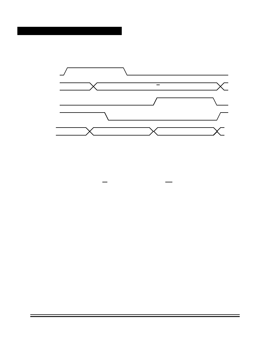
Technical Data
Technical Data
MC68HC(8)05PV8/A -- Rev. 1.9
Fast Parallel Interface
NO
NDISCLOSURE AGREEMENT REQUIRED
Figure 15-1 Basic Fast Peripheral Interface Timing
The basic timing as shown in
Figure 15-1
is similar to the timing used on
the HC11 parts in expanded multiplex mode. At the falling edge of the
address strobe signal (AS/PB0) the addresses on PA0�3, the read/write
signal (RW/PB1) and the chip select (CS/PB3) signal are valid. A high
DEN/PB2 signal indicates that data are driven on the bus in CPU write
cycles or that the peripheral IC can drive data in read cycles. Whenever
the FPICLK bit in the system control register is set the signals become
only active when the range from $0030�$003F is addressed by the CPU
thus significantly reducing electromagnetic noise.
When using the A/D converter in conjunction with the fast peripheral
interface the VRLEN bit of port A configuration register must be cleared.
See
7.4.4 Port A Configuration Register
.
PB0
PA0-3
A0�3
D0�3
RW
CS
PB1
PB2
PB3
AS
DEN
Freescale
Semiconductor,
I
Freescale Semiconductor, Inc.
For More Information On This Product,
Go to: www.freescale.com
nc.
..

Fast Parallel Interface
Description
MC68HC(8)05PV8/A -- Rev. 1.9
Technical Data
Fast Parallel Interface
NO
NDI
S
CLO
S
URE AG
REEMENT
REQ
U
IRED
15.3.1 System Control Register
The following paragraphs describe the FPIE and FPICLK bit function of
the system control register.
FPIE � Fast Peripheral Interface Enable
If this bit is set the fast peripheral interface is enabled. PA0�3 and
PB0�3 are no longer available as I/Os.
1 = Fast peripheral interface enabled
0 = Fast peripheral interface disabled
FPICLK � Fast Peripheral Clock
If this bit is set, the FPI clocks are free running
1 = AS and DEN only become active when CPU accesses
$0030�$003F
0 = AS and DEN always active
$000A
Bit 7
6
5
4
3
2
1
Bit 0
Read:
POR
INTP
INTN
INTE
WCOP
WCP
FPIE
FPICLK
Write:
Reset:
U
0
0
1
0
0
0
0
Figure 15-2 System Control Register (SYSCR)
Freescale
Semiconductor,
I
Freescale Semiconductor, Inc.
For More Information On This Product,
Go to: www.freescale.com
nc.
..

Technical Data
Technical Data
MC68HC(8)05PV8/A -- Rev. 1.9
Fast Parallel Interface
NO
NDISCLOSURE AGREEMENT REQUIRED
Freescale
Semiconductor,
I
Freescale Semiconductor, Inc.
For More Information On This Product,
Go to: www.freescale.com
nc.
..

MC68HC(8)05PV8/A -- Rev. 1.9
Technical Data
Electrical Specifications
NO
NDI
S
CLO
S
URE AG
REEMENT
REQ
U
IRED
Technical Data -- MC68HC(8)05PV8/A
Section 16. Electrical Specifications
16.1 Contents
16.2
Maximum Ratings . . . . . . . . . . . . . . . . . . . . . . . . . . . . . . . . . . 174
16.3
Thermal Characteristics . . . . . . . . . . . . . . . . . . . . . . . . . . . . . 175
16.4
Program and Data EEPROM Characteristics . . . . . . . . . . . . . 175
16.5
Supply Current . . . . . . . . . . . . . . . . . . . . . . . . . . . . . . . . . . . . 176
16.6
V
DD
Referenced Pins Electrical Characteristics . . . . . . . . . . . 178
16.7
Voltage Regulator . . . . . . . . . . . . . . . . . . . . . . . . . . . . . . . . . . 180
16.8
Operational Amplifier . . . . . . . . . . . . . . . . . . . . . . . . . . . . . . . 182
16.9
Power Supply Monitor. . . . . . . . . . . . . . . . . . . . . . . . . . . . . . . 183
16.9.1
V
SUP
related Reset and Interrupts . . . . . . . . . . . . . . . . . . 183
16.10 Down Scaler . . . . . . . . . . . . . . . . . . . . . . . . . . . . . . . . . . . . . . 184
16.11 Die Temperature Monitor . . . . . . . . . . . . . . . . . . . . . . . . . . . . 184
16.12 Control Timing . . . . . . . . . . . . . . . . . . . . . . . . . . . . . . . . . . . . 185
16.13 A/D Converter Characteristics . . . . . . . . . . . . . . . . . . . . . . . . 187
16.14 Fast Peripheral Interface Timing. . . . . . . . . . . . . . . . . . . . . . . 188
16.15 PORT C Characteristics . . . . . . . . . . . . . . . . . . . . . . . . . . . . .189
16.15.1
High Voltage Input/Output (PC0�4). . . . . . . . . . . . . . . . . . 189
16.15.2
Contact Sense Circuitry to Vbattery (PC0�3) and to Ground
(PC1�4 MC68HC(8)05PV8)/(PC1-3 MC68HC05PV8A) . . 189
16.15.3
ISO9141 Driver (PC4) MC68HC(8)05PV8 . . . . . . . . . . . .190
16.15.5
Low Side Driver (PC5/6, PVSS) . . . . . . . . . . . . . . . . . . . . 191
Freescale
Semiconductor,
I
Freescale Semiconductor, Inc.
For More Information On This Product,
Go to: www.freescale.com
nc.
..

Technical Data
Technical Data
MC68HC(8)05PV8/A -- Rev. 1.9
Electrical Specifications
NO
NDISCLOSURE AGREEMENT REQUIRED
16.2 Maximum Ratings
(Voltages referenced to V
SS
)
This device contains circuitry to protect the inputs against damage due
to high static voltages or electric fields. However, it is advised that
normal precautions be taken to avoid application of any voltage higher
than maximum rated voltages to this high-impedance circuit. For proper
operation, it is recommended that LV
IN
is constrained to the range V
SS
LV
IN
V
DD
. Reliability of operation could be affected if unused inputs are
not connected to an appropriate logic voltage level (e.g., either V
SS
or
V
DD
, or V
SS
for the high voltage pins).
Rating
Symbol
Value
Unit
Supply Voltage
V
SUP
�0.3 to +40.0
V
Supply Voltage without using
the Voltage Regulator (V
SUP
= V
DD
)
V
DD
�0.3 to +7.0
V
Input Voltage (PA0�7, PB0�4, OSC1)
LV
IN1
V
SS
�0.3 to V
DD
+0.3
V
Input Voltage (IRQ, RESET)
LV
IN2
V
SS
�0.3 to 12
V
Input Voltage (PC0�3)
HV
IN1
V
SS
�0.3 to V
SUP
+0.3
V
Input Voltage (PC4)
HV
IN2
V
SS
�5 to V
SUP
+0.3
V
Applied Voltage (PC5/6)
HV
IN3
40
V
Applied Voltage (PVSS)
HV
IN4
V
SS
to V
DD
V
Current Drain per Pin
(all I/O, except PC4�6)
I
OUT1
25
mA
Current Drain per Pin (VSUP, VDD, VSS, PC4)
I
OUT2
110
mA
Current Drain per Pin (PC5/6, PVSS)
I
OUT3
700
mA
Operating Junction Temperature Range
T
J
�40 to +125
�
C
Storage Temperature Range
T
STG
�65 to +150
�
C
Freescale
Semiconductor,
I
Freescale Semiconductor, Inc.
For More Information On This Product,
Go to: www.freescale.com
nc.
..
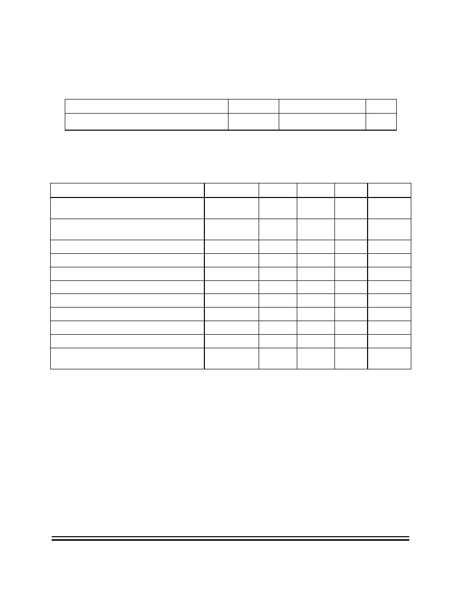
Electrical Specifications
Thermal Characteristics
MC68HC(8)05PV8/A -- Rev. 1.9
Technical Data
Electrical Specifications
NO
NDI
S
CLO
S
URE AG
REEMENT
REQ
U
IRED
16.3 Thermal Characteristics
16.4 Program and Data EEPROM Characteristics
(V
DD
= 5.0Vdc
�
10%, V
SS
= 0Vdc, T
J
= �40
�
C to +125
�
C, unless otherwise noted)
NOTES:
1. Not applicable for MC68HC05PV8
Characteristic
Symbol
Value
Unit
Thermal Resistance SOIC28
JA
60
�
C/W
Rating
Symbol
Min
Max
Unit
Comment
Write/Erase Cycles Program EEPROM
@ 10ms write time, T
J
= +125
�
C
100
-
Cycles
See note 1
Write/Erase Cycles Data EEPROM
@ 10ms write time, T
J
= +125
�
C
10000
-
Cycles
Data Retention EEPROMs
10
-
Years
Program EEPROM Programming Time per 4 Bytes
t
PEEPGM
5
10
ms
See note 1
Program EEPROM Erase Time per 4 Bytes
t
PEBYT
5
10
ms
See note 1
Program EEPROM Bulk Erase Time
t
PEBULK
400
500
ms
See note 1
Data EEPROM Programming Time per Byte
t
EEPGM
5
10
ms
Data EEPROM Erase Time per Byte
t
EBYT
5
10
ms
Data EEPROM Erase Time per Block
t
EBLOCK
5
10
ms
Data EEPROM Bulk Erase Time
t
EBULK
5
10
ms
RC Oscillators Stabilization Time
(Program & Data EEPROM)
t
RCON
5
-
t
CYC
Freescale
Semiconductor,
I
Freescale Semiconductor, Inc.
For More Information On This Product,
Go to: www.freescale.com
nc.
..

Technical Data
Technical Data
MC68HC(8)05PV8/A -- Rev. 1.9
Electrical Specifications
NO
NDISCLOSURE AGREEMENT REQUIRED
16.5 Supply Current
(6V
V
SUP
16V, device untrimmed, V
SS
= 0Vdc, T
J
= �40
�
C to +125
�
C, unless otherwise noted)
NOTES:
1. Typical values reflect average measurements at mid point of supply voltage range (VSUP
= 12V, VDD = 5V) and T
J
= 25
�
C (applies to all tables).
2. Run (Operating), Wait I
SUP
: measured using external square wave clock source to OSC1
(F
OSC
= 4.2 MHz), all inputs 0.2 Vdc from rail; no DC load, all programmable outputs are
static, C
L
= 20 pF on OSC2.
3. Wait, Stop I
SUP
: all ports configured as inputs, LV
IL
= 0.2Vdc, LV
IH
= V
DD
�0.2Vdc, HV
I
=
0.2Vdc.
4. I
SUP1/2/3
are affected by the OSC2 capacitance.
5. Stop I
SUP4
measured with OSC1 = PA0�7 = PB0�4 = IRQ = V
SS
. RESET open.
6. The down scaler is automatically enabled after any reset and can be disabled by setting
Characteristic
Symbol
Typ
Max
Unit
Comment
Full circuit in Run mode
TIMER, A/D, PWM, COP on
I
SUP1
4.4
9
mA
See note 2,4
Full circuit in Wait mode
TIMER, A/D, PWM, COP on
TIMER, A/D, PWM, COP off
I
SUP2
I
SUP3
1.95
1.45
-
-
mA
mA
See notes 2, 3 & 4
Full circuit in Stop mode (PV8)
Port C, Op Amp, Power
Supply Monitor, Temperature
Sensor disabled
I
SUP4
485
650
�
A
See note 5
Full circuit in Stop mode (PV8A)
Port C, Op Amp, Power
Supply Monitor, Temperature
Sensor disabled
I
SUP4A
510
750
�
A
See note 5
Down Scaler Biasing Current
I
SUP5
100
-
�
A
See note 6
Low Side Driver Biasing Current
I
SUP6
280
-
�
A
See notes 7, 8, 13
Contact Sense Circuitry Internal Reference
Biasing Current
I
SUP7
600
-
�
A
See notes 9 & 10
Contact Sense Circuitry to V
BAT
Biasing
Current per Output
I
SUP8B
60
-
�
A
Contact Sense Circuitry to Ground Biasing
Current per Output
I
SUP8G
120
-
�
A
See note 14
ISO9141 Driver Biasing Current On State
I
SUP9
280
-
�
A
See note 11
ISO9141 Driver Biasing Current Off State
I
SUP10
35
-
�
A
Port C Input Biasing Current
I
SUP11
10
-
�
A
See note 12
Ultra Low Power Mode
I
SUP12
35
100
�
A
See note 15, 16, 17
Freescale
Semiconductor,
I
Freescale Semiconductor, Inc.
For More Information On This Product,
Go to: www.freescale.com
nc.
..

Electrical Specifications
Supply Current
MC68HC(8)05PV8/A -- Rev. 1.9
Technical Data
Electrical Specifications
NO
NDI
S
CLO
S
URE AG
REEMENT
REQ
U
IRED
the VSCAL bit in the MFTEST register.
7. Low Side Drivers and Die Temperature Monitor can be disabled by setting LSOFF bit in
the MFTEST register.
8. The Die Temperature Monitor is only disabled when the LSOFF bit is set and the Port C4
DDR bit is cleared as well.
9. There are two common reference blocks for PC0-4, one for contacts to Vbat and one for
contacts to ground.
10. This current is proportional to V
SUP
.
11. The ISO9141 driver can be disabled by clearing the PCDDR4 bit.
12. The Port C Inputs can be disabled by setting the HVTOFF bit in the MFTEST register.
13. Low Side Drivers must be switched off.
14. Comparators are automatically enabled with the corresponding output.
15. Ultra Low Power Mode is only available on MC68HC05PV8A. All I/O pins must be pulled
to levels near VSS or VDD/VSUP resp..
16. 6V < VSUP < 12V.
17. In Ultra Low Power Mode, no external load on VDD, Port A or Port B is allowed.
Freescale
Semiconductor,
I
Freescale Semiconductor, Inc.
For More Information On This Product,
Go to: www.freescale.com
nc.
..

Technical Data
Technical Data
MC68HC(8)05PV8/A -- Rev. 1.9
Electrical Specifications
NO
NDISCLOSURE AGREEMENT REQUIRED
16.6 V
DD
Referenced Pins Electrical Characteristics
(V
DD
= 5.0Vdc
�
10%, V
SS
= 0Vdc, T
J
= �40
�
C to +125
�
C, unless otherwise noted)
Characteristic
Symbol
Min
Typ
Max
Unit
Comment
Output Low Voltage
Port A, Port B
V
OL
1
V
OL
2
�
�
�
�
0.1
0.4
V
V
I
LOAD
= 10
�
A
I
LOAD
= 1.6mA
Output Low Voltage
RESET
V
OL
3
�
�
1
V
I
LOAD
= 1.6mA
Output High Voltage
Port A, Port B
V
OH
1
V
OH
2
V
DD
� 0.1
V
DD
� 0.8
�
�
�
�
V
V
I
LOAD
= �10
�
A
I
LOAD
=�0.8mA
Input High Voltage
Port A, Port B, IRQ, RESET, OSC1
V
IH
0.7xV
DD
�
V
DD
V
Input Low Voltage
Port A, Port B, IRQ, RESET,OSC1
V
IL
V
SS
�
0.3xV
DD
V
Schmitt Trigger Hysteresis
Port A, Port B, IRQ, RESET
V
HYS
�
1
-
V
Input Pull-up Current
PA0�3
I
IN
1
�
80
250
�
A
V
IN
=
V
SS
,
see notes
Input Pull-up Current
PA4�7
I
IN
2
�
0.8
2.5
mA
Input Pull-up Current
PA0�3
I
IN
3
�
50
250
�
A
V
IN
=
0.7xV
DD
,
see notes
Input Pull-up Current
PA4�7
I
IN
4
�
0.5
2.5
mA
Internal Pull-up Resistor
RESET
R
RSTPU
5
19
50
K
Input Current
IRQ, OSC1
I
IN
6
�
�
1
�
A
V
SS
V
IN
V
DD
I/O Ports Hi-Z Leakage Current
Port A, Port B
I
LEAK
�1
�
1
�
A
Pin Capacitance
Port A, Port B, RESET, IRQ
C
PIN
�
�
10
pF
Not tested
Oscillator Transconductance
(I
OSC2
/V
OSC2
)
g
M
0.9
�
�
mA/V
Injection Current
PA1�5
I
INJ
-5
�
5
mA
Not production
tested.
See note 3.
Injection Current
PA0, PA6, PA7
I
INJ
-2
�
2
mA
Injection Current
PB2�4
I
INJ
-1
�
1
mA
Freescale
Semiconductor,
I
Freescale Semiconductor, Inc.
For More Information On This Product,
Go to: www.freescale.com
nc.
..

Electrical Specifications
V
DD
Referenced Pins Electrical Characteristics
MC68HC(8)05PV8/A -- Rev. 1.9
Technical Data
Electrical Specifications
NO
NDI
S
CLO
S
URE AG
REEMENT
REQ
U
IRED
NOTES:
(see next page)
1. The pull-up structures on Port A0�7 can be disabled by software, they are automatically
enabled by each reset.
2. The pull-up structures on Port A consist of enabled PMOS devices. For input voltages near
V
SS
they act like a constant current source.
3. A simple protection can be built with a series resistor: R > V
MAX
/I
INJ
. The sum of currents
during multiple injection should be limited below the maximum values for a single pin:
R > (V
MAX
/I
INJ
)�(number of pins).
Positive injection current can raise the supply voltage (V
DD
). Care must be taken in the ap-
plication to ensure votages do not exceed the maximum ratings.
Characterized on the HC805PV8 and HC05PV8.
Freescale
Semiconductor,
I
Freescale Semiconductor, Inc.
For More Information On This Product,
Go to: www.freescale.com
nc.
..
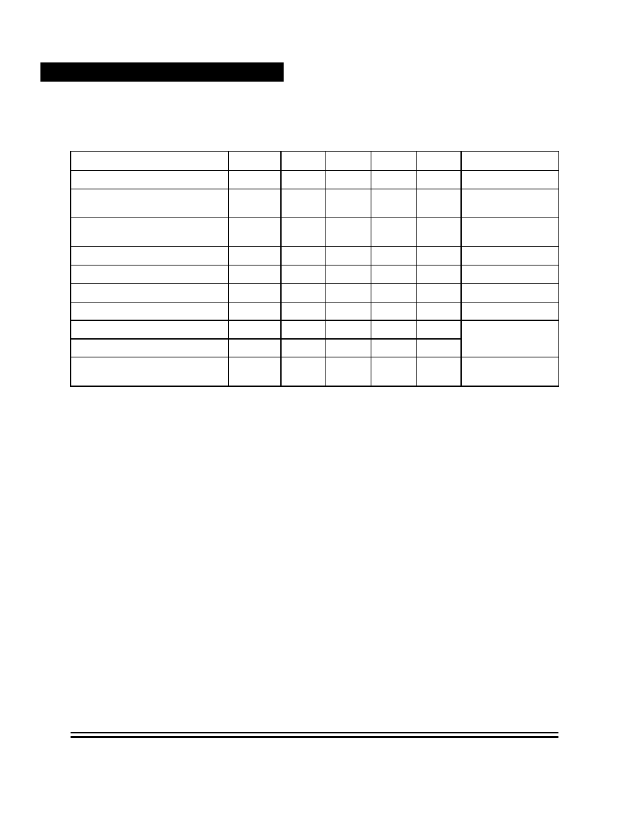
Technical Data
Technical Data
MC68HC(8)05PV8/A -- Rev. 1.9
Electrical Specifications
NO
NDISCLOSURE AGREEMENT REQUIRED
16.7 Voltage Regulator
(6V
V
SUP
16V, device untrimmed, V
SS
= 0Vdc, T
J
= �40
�
C to +125
�
C, unless otherwise noted)
NOTES:
1. The current sourcing capability includes the current for the MCU core, for the ports and
also for any external load.
2. Refer to the maximum power dissipation.
3. The Low Voltage Reset thresholds and hysteresis are measured relative to V
DD
with
VT2..VT0 cleared in the MFTEST register (POR condition, TRIM 0 configuration).
4. As the voltage regulator and the low voltage reset are using the same internal voltage ref-
erence, it is ensured that the low voltage reset will only occur when the voltage regulator
is out of regulation.
5. The stability is ensured with a decoupling capacitor between VDD and VSS: C
OUT
10
�
F
with ESR
10
. Capacitor value and type should be choosen under consideration of the
allowable VDD ripple in the particular application.
Characteristic
Symbol
Min
Typ
Max Unit
Comment
Output Voltage (6V
V
SUP
16V)
V
DD
4.75
5.0
5.25
V
I
OUT
20mA
Output Voltage (9V
V
SUP
16V) in
Ultra Low Power Mode
V
DD
3.7
V
only on
MC68HC05PV8A
Output Voltage
(5.5V < V
SUP
40V)
V
DD
4.5
5.0
5.5
V
I
OUT
30mA
Total Output Current
I
OUT
�
�
30
mA
See notes 1 & 2
Line Regulation (6V
V
SUP
16V)
V
L
I
R
�
10
35
mV
I
OUT
= 1mA
Load Regulation
V
L
O
R
�
50
100
mV
1mA
I
OUT
20mA
Output Voltage Trimming Step
V
S
TEP
T
RIM
-
40
-
mV
See chapter 12
Low Voltage Reset Low Threshold
V
LVRON
4.15
4.40
4.65
V
See notes 3, 4
&
Figure 16-1
Low Voltage Reset Hysteresis
V
LVRH
40
100
200
mV
Low Voltage Reset Low Threshold in
Ultra Low Power Mode
V
ULVRON
2.6
V
only on
MC68HC05PV8A
Freescale
Semiconductor,
I
Freescale Semiconductor, Inc.
For More Information On This Product,
Go to: www.freescale.com
nc.
..

Electrical Specifications
Voltage Regulator
MC68HC(8)05PV8/A -- Rev. 1.9
Technical Data
Electrical Specifications
NO
NDI
S
CLO
S
URE AG
REEMENT
REQ
U
IRED
Figure 16-1 Low Voltage Reset waveform
V
DD
RESET
V
LVRON
V
LVRON
+ V
LVRH
Freescale
Semiconductor,
I
Freescale Semiconductor, Inc.
For More Information On This Product,
Go to: www.freescale.com
nc.
..

Technical Data
Technical Data
MC68HC(8)05PV8/A -- Rev. 1.9
Electrical Specifications
NO
NDISCLOSURE AGREEMENT REQUIRED
16.8 Operational Amplifier
(device untrimmed, V
SS
= 0Vdc, T
J
= �40
�
C to +125
�
C, unless otherwise noted)
Characteristic
Symbol
Min
Typ
Max Unit
Comment
Input Offset Voltage
V
IO
�
1
20
mV
Input Common Mode Voltage Range
V
ICR
V
SS
�
V
DD
�
1.2
V
Large Signal Gain
A
VOL
�
30
�
V/mV
Output Voltage Swing
V
OH
V
SS
..
V
DD
�
0.2
V
R
LOAD
= 50K
to VSS
Output Short Circuit Current to V
SS
I
SCG
�
5
�
mA
V
ID
= 1V, V
O
= V
SS
,
T
J
= 25
�
C
Output Short Circuit Current to V
DD
I
SCP
�
50
�
�
A
V
ID
= �1V, V
O
= V
DD
,
T
J
= 25
�
C
Slew Rate
SR
�
1
�
V/
�
s
V
IN
= 0.5V to 4.5V,
R
LOAD
= 50K
to
VSS, C
LOAD
= 25pF
Gain Bandwidth Product
GBW
�
1
�
MHz
f = 10KHz
Freescale
Semiconductor,
I
Freescale Semiconductor, Inc.
For More Information On This Product,
Go to: www.freescale.com
nc.
..

Electrical Specifications
Power Supply Monitor
MC68HC(8)05PV8/A -- Rev. 1.9
Technical Data
Electrical Specifications
NO
NDI
S
CLO
S
URE AG
REEMENT
REQ
U
IRED
16.9 Power Supply Monitor
16.9.1 V
SUP
related Reset and Interrupts
(device untrimmed, V
SS
= 0Vdc, T
J
= �40
�
C to +125
�
C, unless otherwise noted)
NOTE:
See chapter
16.7
for the Low Voltage Reset function.
Figure 16-2 VSUP related Reset and Interrupts waveforms
Characteristic
Symbol
Min
Typ
Max
Unit
Comment
High Voltage Reset On
V
HVRON
34.5
36
37.5
V
S
EE
Figure 16-2
High Voltage Reset Hysteresis
V
HVRH
-
1.5
-
V
High Voltage Interrupt On
V
HVION
29
30.5
32
V
High Voltage Interrupt Hysteresis
V
HVIH
-
1.5
-
V
Low Voltage Interrupt On
V
LVION
6.5
7.5
8.5
V
Low Voltage Interrupt Hysteresis
V
LVIH
-
0.6
-
V
V
SUP
V
HVRON
� V
HVRH
V
HVRON
V
HVION
� V
HVIH
V
HVION
V
LVION
V
LVION
+ V
LVIH
High Voltage Reset
High Voltage Interrupt
Low Voltage Interrupt
Freescale
Semiconductor,
I
Freescale Semiconductor, Inc.
For More Information On This Product,
Go to: www.freescale.com
nc.
..

Technical Data
Technical Data
MC68HC(8)05PV8/A -- Rev. 1.9
Electrical Specifications
NO
NDISCLOSURE AGREEMENT REQUIRED
16.10 Down Scaler
(device untrimmed, V
SS
= 0Vdc, T
J
= �40
�
C to +125
�
C, unless otherwise noted)
NOTE:
1. The Down Scaler output is internally clamped at 5.3V typical.
2. The Down Scaler can only be observed by the A/D. The errors of the A/D has to be taken
into account.
16.11 Die Temperature Monitor
(device untrimmed, V
SS
= 0Vdc, unless otherwise noted)
NOTE:
1. By design the High Temperature Reset threshold is guaranteed to be (typically 25
�
C)
above the High Temperature Interrupt threshold.
2. Functionality of the device is not guaranteed for T
J
125
�
C. See absolute maximum rat-
ings.
3. Measured on final test with VDD forced to 5.0V and ATD switched to internal reference.
P
tot
~ 100mW.
Characteristic
Symbol
Min
Typ
Max Unit
Comment
Voltage Ratio
=
V
SUP
/V
AD7
4.85
5.1
5.35
�
6V
V
SUP
25.5V,
See note 1,2
and chapter 10
Characteristic
Symbol
Min
Typ
Max
Unit
Comment
High Temperature Reset On
T
HTRON
�
150
�
�
C
See note 1 & 2
High Temperature Reset Hysteresis
T
HTRH
�
7
�
�
C
High Temperature Interrupt On
T
HTION
�
125
�
�
C
High Temperature Interrupt Hystere-
sis
T
HTIH
�
7
�
�
C
Temperature Sensor A/D Reading
N
TSOUT
�
142
�
-
T
J
= 25
�
C
Temperature Sensor A/D Reading
N
TSOUT
171
202
-
T
A
= 125
�
C, note 3
Temperature Sensor Output
Sensitivity (A/D Reading)
S
�
0.45
�
1/
�
C
�40
�
C
T
J
+125
�
C
Freescale
Semiconductor,
I
Freescale Semiconductor, Inc.
For More Information On This Product,
Go to: www.freescale.com
nc.
..

Electrical Specifications
Control Timing
MC68HC(8)05PV8/A -- Rev. 1.9
Technical Data
Electrical Specifications
NO
NDI
S
CLO
S
URE AG
REEMENT
REQ
U
IRED
16.12 Control Timing
(V
DD
= 5.0Vdc
�
10%, V
SS
= 0Vdc, T
J
= �40
�
C to +125
�
C, unless otherwise noted)
NOTES:
1. The minimum period t
ILIL
or t
IHIH
should not be less than the number of cycles it takes to
execute the interrupt service routine plus 19 t
CYC
.
2. The 2-bit timer prescaler is the limiting factor in determining timer resolution.
3. The minimum period t
TLTL
should not be less than the number of cycles it takes to execute
the capture interrupt service routine plus 24 t
CYC
.
Characteristic
Symbol
Min
Max
Unit
Frequency of Operation
Crystal Oscillator Option
(i.e. using the oscillator with a crystal)
External Clock Source
Oscillator Frequency With Enabled Clock Monitor
f
OSC
f
OSC
f
OSC
0.1
dc
0.4
4.2
4.2
4.2
MHz
MHz
MHz
Cycle Time (2/f
OSC
)
t
CYC
476
�
ns
Frequency Detected As Clock Monitor Error
f
OSC
dc
10
KHz
Clock Monitor Backup-Oscillator Frequency
f
OSC
0.8
4.2
MHz
Crystal Oscillator Start-up Time
t
OXON
�
100
ms
Stop Recovery Start-up Time
t
ILCH
�
100
ms
RESET Pulse Width Low
t
RL
120
�
ns
Interrupt Pulse Width Low (Edge-Triggered)
t
ILIH
120
�
ns
Interrupt Pulse Period
t
ILIL
note 1
�
t
CYC
OSC1 Pulse Width
t
OSC1
90
�
ns
Supply rise slew rate for POR detection
S
RISE
0.1
�
V/
�
s
16 bit Timer
Resolution (note 2)
Input Capture Pulse Width
Input Capture Period
t
RESL
t
TH
, t
TL
t
TLTL
4.0
85
note 3
�
�
�
t
CYC
ns
t
CYC
Freescale
Semiconductor,
I
Freescale Semiconductor, Inc.
For More Information On This Product,
Go to: www.freescale.com
nc.
..
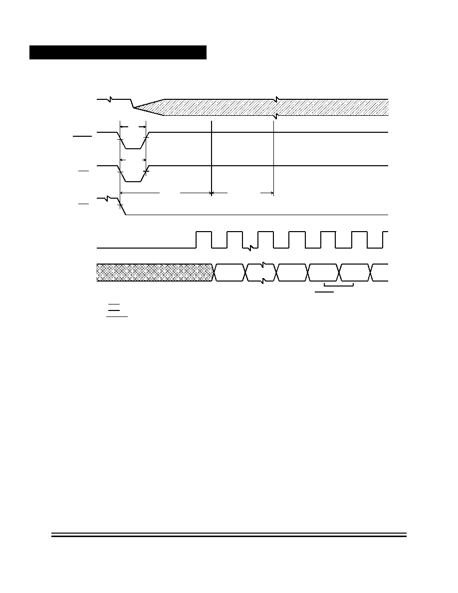
Technical Data
Technical Data
MC68HC(8)05PV8/A -- Rev. 1.9
Electrical Specifications
NO
NDISCLOSURE AGREEMENT REQUIRED
Figure 16-3 Stop Recovery Timing Diagram
3FFE
3FFE
3FFE
3FFE
3FFF
t
RL
t
ILIH
OSC1
1
RESET
IRQ
2
IRQ
3
Internal
Clock
Internal
Address
Bus
t
ILCH
4064 t
CYC
NOTES:
1. Represents the internal gating of the OSC1 pin
2. IRQ pin edge-sensitive selected.
3. IRQ pin level and edge-sensitive selected.
4.RESET vector address shown for timing example.
RESET or Interrupt
Vector Fetch
Freescale
Semiconductor,
I
Freescale Semiconductor, Inc.
For More Information On This Product,
Go to: www.freescale.com
nc.
..

Electrical Specifications
A/D Converter Characteristics
MC68HC(8)05PV8/A -- Rev. 1.9
Technical Data
Electrical Specifications
NO
NDI
S
CLO
S
URE AG
REEMENT
REQ
U
IRED
16.13 A/D Converter Characteristics
(V
REFH
= V
DD
= 5.0Vdc
�
10%, V
REFL
= 0Vdc, T
J
= �40
�
C to +125
�
C, unless otherwise noted
)
NOTE:
1. t
AD
is either the bus clock period or the RC oscillator period (600ns typical).
Characteristic
Symbol
Min
Max
Unit
Comment
Resolution
�
8
bit
Absolute Accuracy
�
�
1.5
LSB
Including quantization error
Conversion Range
Voltage Reference High Level
Voltage Reference Low Level
V
REFH
V
REFL
V
REFL
V
REFL
V
SS
V
REFH
V
DD
V
REFH
V
V
V
A/D accuracy may decrease
proportionately as V
REFH
is
reduced below V
DD
Analog Input Voltage
�
V
REFL
V
REFH
V
Must be within V
SS
and V
DD
Zero Input Reading
�
00
01
Hex
V
IN
= V
REFL
Full-scale Reading
�
FE
FF
Hex
V
IN
= V
REFH
Conversion Time
(Including Sampling Time)
T
C
ONV
32
t
AD
See note
Sampling Time
T
S
AMP
12
t
AD
Power-up Time
�
�
100
�
s
A/D On Current Stabilization Time
t
ADON
�
100
�
s
RC Oscillator Stabilization Time
t
RCON
�
5
�
s
A/D Capacitance
C
AD
�
8
pF
Not tested
Freescale
Semiconductor,
I
Freescale Semiconductor, Inc.
For More Information On This Product,
Go to: www.freescale.com
nc.
..

Technical Data
Technical Data
MC68HC(8)05PV8/A -- Rev. 1.9
Electrical Specifications
NO
NDISCLOSURE AGREEMENT REQUIRED
16.14 Fast Peripheral Interface Timing
(V
DD
= 5.0Vdc
�
10%, V
SS
= 0Vdc, T
J
= �40
�
C to +125
�
C, unless otherwise noted)
NOTES:
1. The first cycle denotes a read, the second a write cycle.
2. Unlike in the HC11 AS and DEN occur only when accessing the external memory if not
enabled continuously.
3. OSC1/OSC2 input clock other than 50% duty cycle affect bus performance.
4. All timing is shown with respect to 20% V
DD
and 70% V
DD
, unless otherwise noted.
Figure 16-4 Timing definition
Characteristic
Symbol
Min
Max
Unit
Comment
DEN/AS Rise and Fall Time
t
R
t
F
-
-
25
25
ns
ns
See
Pulse Width AS, DEN high
PW
210
-
ns
See
Address, CS, RW setup time
t
AS
49
-
ns
See
Address, CS, RW hold time
t
AH
22
-
ns
See
Read data setup time
t
DSR
100
-
ns
See
Read data hold time
t
DHR
50
-
ns
See
Write data setup time
t
DSW
30
-
ns
See
Write data hold time
t
DHW
30
-
ns
See
PB0/AS
PB1/RW
A3:0
PA3:0
1
PB2/DEN
1
2
3
4
D3:0
R/W
A3:0
1
1
5
6
R/W
D3:0
7
8
PB3/CS
Freescale
Semiconductor,
I
Freescale Semiconductor, Inc.
For More Information On This Product,
Go to: www.freescale.com
nc.
..
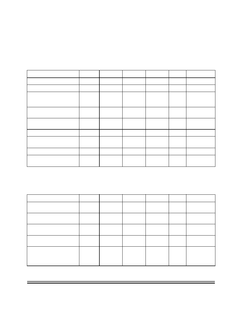
Electrical Specifications
PORT C Characteristics
MC68HC(8)05PV8/A -- Rev. 1.9
Technical Data
Electrical Specifications
NO
NDI
S
CLO
S
URE AG
REEMENT
REQ
U
IRED
16.15 PORT C Characteristics
16.15.1 High Voltage Input/Output (PC0�4)
(6V
V
SUP
16V, device untrimmed, V
SS
= 0Vdc, T
J
= �40
�
C to +125
�
C, unless otherwise noted)
,
16.15.2 Contact Sense Circuitry to Vbattery (PC0�3) and to Ground (PC1�4
MC68HC(8)05PV8)/(PC1-3 MC68HC05PV8A)
(9V
V
SUP
16V, device untrimmed, V
SS
= 0Vdc, T
J
= �40
�
C to +125
�
C, unless otherwise noted)
Characteristic
Symbol
Min
Typ
Max
Unit
Comment
Input Low Voltage
HV
IL
0
�
0.35 x V
SUP
V
Input High Voltage
HV
IH
0.65 x V
SUP
�
V
SUP
V
Input Hysteresis Voltage
(PC0-3, PC4 on
MC68HC(8)05PV8)
V
HYS
0.1
0.1 x V
SUP
�
V
Leakage Current
I
L
EAK
�10
�
10
�
A
Inputs
disabled
Input Pull-Down Current
I
P
ULL
D
OWN
�
2.5
10
�
A
Inputs enabled,
V
IN
= V
SUP
Output Low Voltage (PC0�3)
V
OL
�
-
0.2 x V
SUP
V
I
LOAD
= 1mA
Output High Voltage (PC0�4)
(PC0-3 MC68HC05PV8A)
V
OH
0.8 x V
SUP
-
�
V
I
LOAD
= �1mA
Pin Capacitance
C
OUT
�
�
10
pF
Not tested
Debounce Time
(PC4 on MC68HC05PV8A)
t
DB
1.5
�
s
Not tested
Characteristic
Symbol
Min
Typ
Max
Unit
Comment
Effective Internal Input
Resistance
R
IN
�
�
600
|I
LOAD
| = 5mA
Total Path Resistance for Low
Threshold
R
LT
2.5
4.0
�
K
Total Path Resistance for High
Threshold
R
HT
�
6.0
10.0
K
Total Path Resistance
Hysteresis
R
LT
/R
HT
�
0.75
�
�
Injection Current
I
INJ
-5
�
5
mA
Not production
tested. See also
note 3 on page
179.
Freescale
Semiconductor,
I
Freescale Semiconductor, Inc.
For More Information On This Product,
Go to: www.freescale.com
nc.
..
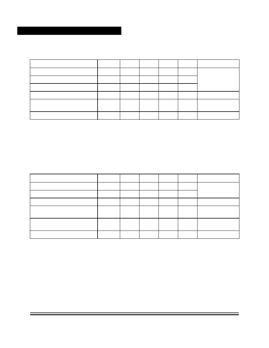
Technical Data
Technical Data
MC68HC(8)05PV8/A -- Rev. 1.9
Electrical Specifications
NO
NDISCLOSURE AGREEMENT REQUIRED
16.15.3 ISO9141 Driver (PC4) MC68HC(8)05PV8
(6V
V
SUP
16V, device untrimmed, V
SS
= 0Vdc, T
J
= �40
�
C to +125
�
C, unless otherwise noted
NOTES:
1. The ISOMODE bit in PORTC CONFIG0 register must be set.
2. Calculated from 20% to 80% of the output swing.
3. PC4 is not short circuit protected to VSUP.
16.15.4 ISO9141 Driver (PC4) MC68HC05PV8A
(6V
V
SUP
16V, device untrimmed, V
SS
= 0Vdc, T
J
= �40
�
C to +125
�
C, unless otherwise noted
Characteristic
Symbol
Min
Typ
Max Unit
Comment
Output Falling Edge Slew Rate
SR
F
3
5
7
V/
�
s
R
Pull-up
= 510
,
See note 2
Output Rising Edge Slew Rate
SR
R
3
5
7
V/
�
s
Rise Fall Slew Rates Symmetry
SR
�1
0
1
V/
�
s
Output Low Voltage
V
OL
�
1
1.3
V
I
LOAD
= 25mA
Leakage Current (driver switched
recessive)
I
LEAK
-10
10
�
A
-5V
V
IN
V
SUP
Current Limitation Threshold
I
LIM
40
55
-
mA
See note 3
Characteristic
Symbol
Min
Typ
Max Unit
Comment
Output Falling Edge Slew Rate
SR
F
-3.25
-2.25
-1.5
V/
�
s
R
Pull-up
= 510
,
See note 2
Output Rising Edge Slew Rate
SR
R
1.5
2.25
3.25
V/
�
s
Output Low Voltage
V
OL
�
1
1.4
V
I
LOAD
= 25mA
Leakage Current (driver switched
recessive)
I
LEAK
-10
10
�
A
0V
V
IN
V
SUP
Input Current (driver switched reces-
sive)
I
LEAK
-10
V
IN
/5K
0.01
mA
-16V
V
IN
0V
Device powered
Current Limitation Threshold
I
LIM
40
55
-
mA
See note 3
Freescale
Semiconductor,
I
Freescale Semiconductor, Inc.
For More Information On This Product,
Go to: www.freescale.com
nc.
..
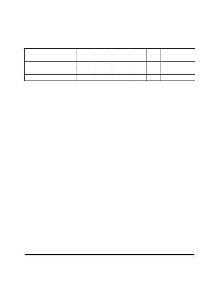
Electrical Specifications
PORT C Characteristics
MC68HC(8)05PV8/A -- Rev. 1.9
Technical Data
Electrical Specifications
NO
NDI
S
CLO
S
URE AG
REEMENT
REQ
U
IRED
16.15.5 Low Side Driver (PC5/6, PVSS)
(6V
V
SUP
16V, device untrimmed,
Vss = 0 Vdc, T
J
= �40
�
C to +125
�
C, unless otherwise noted)
Characteristic
Symbol
Min
Typ
Max
Unit
Comments
Output Resistance
R
DS_ON
�
2
4
I
LOAD
= 100mA
Leakage Current
I
L
EAK
�10
�
10
�
A
0V
V
IN
16V
Positive Output Clamp Voltage
V
C
LAMP
40
42.5
45
V
Over Current Threshold Shutdown
I
S
HUT
D
OWN
300
500
700
mA
Freescale
Semiconductor,
I
Freescale Semiconductor, Inc.
For More Information On This Product,
Go to: www.freescale.com
nc.
..

Technical Data
Technical Data
MC68HC(8)05PV8/A -- Rev. 1.9
Electrical Specifications
NO
NDISCLOSURE AGREEMENT REQUIRED
Freescale
Semiconductor,
I
Freescale Semiconductor, Inc.
For More Information On This Product,
Go to: www.freescale.com
nc.
..

MC68HC(8)05PV8/A -- Rev. 1.9
Technical Data
NO
NDI
S
CLO
S
URE AG
REEMENT
REQ
U
IRED
APPENDIX B
ELECTRICAL SPECIFICATION FOR CURRENT
COMMUNICATION INTERFACE
B.1
Current Interface (PC5 or 6, PVSS)
(6V
V
SUP
16V, device untrimmed
,
Vss = 0 Vdc, T
J
= -40
o
C to +125
o
C,
unless otherwise noted)
NOTE :
1. With an external serial resistor 82.6
�
1%(typically) between PVSS and VSS.
Characteristic
Symbol
Min
Typ
Max
Unit
Comments
Output Current
I
LIM2
30
35
40
mA
See note 1
Freescale
Semiconductor,
I
Freescale Semiconductor, Inc.
For More Information On This Product,
Go to: www.freescale.com
nc.
..

Technical Data
Technical Data
MC68HC(8)05PV8/A -- Rev. 1.9
NO
NDISCLOSURE AGREEMENT REQUIRED
Freescale
Semiconductor,
I
Freescale Semiconductor, Inc.
For More Information On This Product,
Go to: www.freescale.com
nc.
..

F
r
e
e
s
c
a
l
e
S
e
m
i
c
o
n
d
u
c
t
o
r
,
I
Freescale Semiconductor, Inc.
For More Information On This Product,
Go to: www.freescale.com
n
c
.
.
.

MC68HC05PV8/D
REV 1.9
F
r
e
e
s
c
a
l
e
S
e
m
i
c
o
n
d
u
c
t
o
r
,
I
Freescale Semiconductor, Inc.
For More Information On This Product,
Go to: www.freescale.com
n
c
.
.
.
Home Page:
www.freescale.com
email:
support@freescale.com
USA/Europe or Locations Not Listed:
Freescale Semiconductor
Technical Information Center, CH370
1300 N. Alma School Road
Chandler, Arizona 85224
(800) 521-6274
480-768-2130
support@freescale.com
Europe, Middle East, and Africa:
Freescale Halbleiter Deutschland GmbH
Technical Information Center
Schatzbogen 7
81829 Muenchen, Germany
+44 1296 380 456 (English)
+46 8 52200080 (English)
+49 89 92103 559 (German)
+33 1 69 35 48 48 (French)
support@freescale.com
Japan:
Freescale Semiconductor Japan Ltd.
Headquarters
ARCO Tower 15F
1-8-1, Shimo-Meguro, Meguro-ku
Tokyo 153-0064, Japan
0120 191014
+81 2666 8080
support.japan@freescale.com
Asia/Pacific:
Freescale Semiconductor Hong Kong Ltd.
Technical Information Center
2 Dai King Street
Tai Po Industrial Estate,
Tai Po, N.T., Hong Kong
+800 2666 8080
support.asia@freescale.com
For Literature Requests Only:
Freescale Semiconductor
Literature Distribution Center
P.O. Box 5405
Denver, Colorado 80217
(800) 441-2447
303-675-2140
Fax: 303-675-2150
LDCForFreescaleSemiconductor
@hibbertgroup.com
Information in this document is provided solely to enable system and software
implementers to use Freescale Semiconductor products. There are no express or
implied copyright licenses granted hereunder to design or fabricate any integrated
circuits or integrated circuits based on the information in this document.
Freescale Semiconductor reserves the right to make changes without further notice to
any products herein. Freescale Semiconductor makes no warranty, representation or
guarantee regarding the suitability of its products for any particular purpose, nor does
Freescale Semiconductor assume any liability arising out of the application or use of
any product or circuit, and specifically disclaims any and all liability, including without
limitation consequential or incidental damages. "Typical" parameters which may be
provided in Freescale Semiconductor data sheets and/or specifications can and do
vary in different applications and actual performance may vary over time. All operating
parameters, including "Typicals" must be validated for each customer application by
customer's technical experts. Freescale Semiconductor does not convey any license
under its patent rights nor the rights of others. Freescale Semiconductor products are
not designed, intended, or authorized for use as components in systems intended for
surgical implant into the body, or other applications intended to support or sustain life,
or for any other application in which the failure of the Freescale Semiconductor product
could create a situation where personal injury or death may occur. Should Buyer
purchase or use Freescale Semiconductor products for any such unintended or
unauthorized application, Buyer shall indemnify and hold Freescale Semiconductor
and its officers, employees, subsidiaries, affiliates, and distributors harmless against all
claims, costs, damages, and expenses, and reasonable attorney fees arising out of,
directly or indirectly, any claim of personal injury or death associated with such
unintended or unauthorized use, even if such claim alleges that Freescale
Semiconductor was negligent regarding the design or manufacture of the part.
RoHS-compliant and/or Pb- free versions of Freescale products have the functionality
and electrical characteristics of their non-RoHS-compliant and/or non-Pb- free
counterparts. For further information, see http://www.freescale.com or contact your
Freescale sales representative.
For information on Freescale.s Environmental Products program, go to
http://www.freescale.com/epp.