
� Freescale Semiconductor, Inc., 2005. All rights reserved.
Freescale Semiconductor
Technical Data
The MPC7455 and MPC7445 are implementations of the
PowerPCTM microprocessor family of reduced instruction set
computer (RISC) microprocessors. This document is primarily
concerned with the MPC7455; however, unless otherwise noted,
all information here also applies to the MPC7445. This document
describes pertinent electrical and physical characteristics of the
MPC7455. For functional characteristics of the processor, refer to
the MPC7450 RISC Microprocessor Family User's Manual. To
locate any published updates for this document, refer to the
website at http://www.freescale.com.
1
Overview
The MPC7455 is the third implementation of the fourth generation
(G4) microprocessors from Freescale. The MPC7455 implements
the full PowerPC 32-bit architecture and is targeted at networking
and computing systems applications. The MPC7455 consists of a
processor core, a 256-Kbyte L2, and an internal L3 tag and
controller which support a glueless backside L3 cache through a
dedicated high-bandwidth interface. The MPC7445 is identical to
the MPC7455 except it does not support the L3 cache interface.
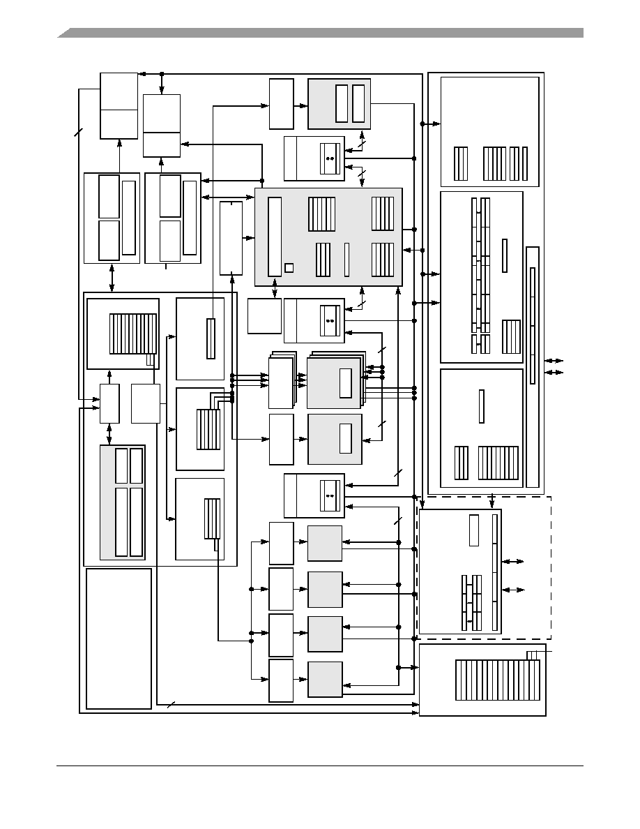
Figure 1
shows a block diagram of the MPC7455.
MPC7455EC
Rev. 4.1, 02/2005
Contents
1. Overview . . . . . . . . . . . . . . . . . . . . . . . . . . . . . . . . . . . 1
2. Features . . . . . . . . . . . . . . . . . . . . . . . . . . . . . . . . . . . . 3
3. Comparison with the MPC7400, MPC7410,
MPC7450, MPC7451, and MPC7441 . . . . . . . . . . . . . 7
4. General Parameters . . . . . . . . . . . . . . . . . . . . . . . . . . . 9
5. Electrical and Thermal Characteristics . . . . . . . . . . . 10
6. Pin Assignments . . . . . . . . . . . . . . . . . . . . . . . . . . . . 33
7. Pinout Listings . . . . . . . . . . . . . . . . . . . . . . . . . . . . . 35
8. Package Description . . . . . . . . . . . . . . . . . . . . . . . . . 41
9. System Design Information . . . . . . . . . . . . . . . . . . . 45
10. Document Revision History . . . . . . . . . . . . . . . . . . . 59
11. Ordering Information . . . . . . . . . . . . . . . . . . . . . . . . 60
MPC7455
RISC Microprocessor
Hardware Specifications
MPC7455 RISC Microprocessor Hardware Specifications, Rev. 4.1
2
Freescale Semiconductor
Overview
Figure 1. MPC7455 Block Diagram
+
In
t
e
g
e
r
R
e
s
e
r
v
ati
on
St
a
t
i
o
n
Un
it
2
+
In
t
e
g
e
r
R
e
s
e
r
v
at
i
o
n
St
a
t
i
o
n
Un
it
2
A
d
dit
i
on
a
l
Fe
a
t
ur
e
s
�
T
im
e B
a
s
e
C
o
u
n
t
er
/
D
ec
r
e
me
nt
er
�
C
lo
c
k
Mu
lt
i
p
l
i
e
r
�
J
T
A
G
/
C
O
P
In
te
r
f
a
c
e
�
T
he
r
m
al
/
P
o
w
er
Ma
na
ge
m
e
n
t
�
P
er
f
o
r
m
an
c
e
M
o
ni
t
o
r
+
+
x �
FP
S
C
R
FP
S
C
R
PA
+x
�
In
st
r
u
ct
io
n
Un
it
I
n
s
t
r
u
c
t
i
o
n Q
u
eu
e
(
12-
W
o
r
d
)
96-
B
i
t (
3
In
s
t
r
u
c
t
i
o
n
s
)
R
e
s
e
r
v
ati
on
In
t
e
g
e
r
1
28-
B
i
t (
4
Ins
t
r
u
c
t
i
ons
)
32-
B
i
t
Fl
oa
ti
ng
-
P
o
in
t
Un
it
64
-
B
i
t
R
e
s
e
r
v
ati
on
Loa
d/
S
t
o
r
e
U
n
i
t
(
EA C
a
lc
u
l
a
t
io
n
)
F
i
ni
s
hed
32
-
B
i
t
Co
m
p
le
t
i
o
n
Un
it
C
o
mp
l
e
ti
on Q
ueu
e
(1
6
-
E
n
t
r
y
)
Ta
g
s
32-
K
b
y
t
e
D Ca
c
h
e
L
3
C
ach
e C
o
n
t
r
o
ller
S
y
st
em
B
u
s In
t
e
r
f
ace
3
6
-
B
i
t
A
ddr
es
s
B
u
s
64-
B
i
t D
a
ta B
u
s
18
-
B
i
t
64-
B
i
t Data
In
t
e
g
e
r
S
t
ati
ons
(
2
)
R
e
s
e
r
v
ati
on
St
a
t
i
o
n
R
e
s
e
r
v
at
i
on
S
t
ati
ons
(
2
)
FP
R
Fi
l
e
1
6
R
enam
e
B
u
ffer
s
S
t
ati
ons
(
2
-
E
ntr
y
)
GP
R
F
i
l
e
1
6
R
ena
me
B
u
ffer
s
R
e
s
e
r
v
at
i
o
n
St
a
t
i
o
n
VR
F
i
le
16 R
e
name
Bu
f
f
e
r
s
64
-
B
i
t
128-
B
i
t
128
-
B
i
t
Com
p
l
e
te
s
up
to thr
e
e
i
n
s
t
r
u
c
t
i
ons
per
c
l
oc
k
C
o
m
p
l
e
ted
In
st
r
u
ct
io
n
MMU
SR
s
(
S
hadow
)
12
8-
E
n
tr
y
IB
A
T
A
r
r
a
y
IT
L
B
T
ags
32-
K
b
y
t
e
I Cac
h
e
S
t
or
es
S
t
or
es
Load Mi
s
s
Ve
c
t
o
r
To
u
c
h
Q
ueue
(3
)
V
R
Is
s
u
e
F
P
R
Is
s
u
e
B
r
a
n
c
h
P
r
o
ces
sin
g
U
n
it
CT
R
LR
B
T
I
C
(
1
28-
E
n
tr
y
)
B
H
T
(
2
0
48-
E
n
tr
y
)
F
e
tc
her
GP
R
I
ssu
e
(6
-E
n
t
ry
/
3
-I
s
s
u
e
)
(4
-E
n
t
r
y
/
2
-I
s
s
u
e
)
(
2
-
E
n
t
r
y
/
1
-
I
s
s
u
e
)
D
i
s
patc
h
Un
i
t
256-
K
b
yt
e U
n
if
i
e
d
L
2
C
ach
e/C
a
c
h
e
C
o
n
t
r
o
ller
Da
t
a
M
M
U
SR
s
(Or
i
g
i
n
a
l
)
1
28-
E
n
tr
y
DB
A
T
A
r
r
a
y
DT
L
B
V
e
c
t
or
T
ouc
h
E
n
g
i
ne
32-
B
i
t
EA
L1 C
a
s
t
out
S
t
at
us
L
2
S
t
o
r
e Q
u
eu
e (
L
2S
Q
)
Ex
t
e
r
n
a
l
SR
A
M
L3
C
R
(8
-
B
i
t
P
a
ri
t
y
)
Ad
d
r
e
s
s
V
ect
o
r
FP
U
R
e
s
e
r
v
ati
on
St
a
t
i
o
n
R
e
s
e
r
v
ati
on
St
a
t
i
o
n
R
e
s
e
r
v
ati
o
n
St
a
t
i
o
n
Ve
c
t
o
r
In
t
e
g
e
r
Un
i
t
1
Ve
c
t
o
r
In
t
e
g
e
r
Un
it
2
V
ect
o
r
Pe
r
m
u
t
e
Un
it
Li
ne
S
t
at
us
Ta
g
s
Bu
s
A
c
c
u
m
u
l
a
t
o
r
Ta
g
s
B
l
o
ck 0
(
32-
B
y
t
e
)
St
a
t
u
s
B
l
o
ck 1 (
32-
B
y
t
e
)
B
l
oc
k
0/
1
Li
ne
Mem
o
r
y
S
u
b
s
yst
em
L1
Load
Q
u
e
ue (
LLQ
)
L1 Load
M
i
s
s
(
5
)
C
a
c
heab
l
e
S
t
o
r
e
Ins
t
r
u
c
t
i
on F
e
t
c
h (
2
)
R
equ
es
t (
1
)
L
1
S
e
r
v
ice
Q
u
eu
es
S
noop P
u
s
h
/
Int
e
r
v
ent
i
ons
L1 S
t
or
e
Q
u
eue
L1 C
a
s
t
outs
Pu
s
h
Ca
s
t
o
u
t
Qu
e
u
e
B
u
s
S
t
or
e Q
u
eu
e
L2 P
r
e
f
etc
h
(
3
)
Bu
s
Ac
c
u
m
u
l
a
t
o
r
(
1
or
2 M
b
y
t
e
s
)
(L
S
Q
)
L1
P
u
s
h
(4
)
(9
)
Un
it
2
U
n
i
t
1
No
t
i
n
MP
C
7
44
5

MPC7455 RISC Microprocessor Hardware Specifications, Rev. 4.1
Freescale Semiconductor
3
Features
The core is a high-performance superscalar design supporting a double-precision floating-point unit and a SIMD
multimedia unit. The memory storage subsystem supports the MPX bus protocol and a subset of the 60x bus protocol
to main memory and other system resources. The L3 interface supports 1 or 2 Mbytes of external SRAM for L3
cache data.
Note that the MPC7455 is footprint-compatible with the MPC7450 and MPC7451, and the MPC7445 is
footprint-compatible with the MPC7441.
2
Features
This section summarizes features of the MPC7455 implementation of the PowerPC architecture.
Major features of the MPC7455 are as follows:
�
High-performance, superscalar microprocessor
-- As many as four instructions can be fetched from the instruction cache at a time
-- As many as three instructions can be dispatched to the issue queues at a time
-- As many as 12 instructions can be in the instruction queue (IQ)
-- As many as 16 instructions can be at some stage of execution simultaneously
-- Single-cycle execution for most instructions
-- One instruction per clock cycle throughput for most instructions
-- Seven-stage pipeline control
�
Eleven independent execution units and three register files
-- Branch processing unit (BPU) features static and dynamic branch prediction
� 128-entry (32-set, four-way set-associative) branch target instruction cache (BTIC), a cache of
branch instructions that have been encountered in branch/loop code sequences. If a target instruction
is in the BTIC, it is fetched into the instruction queue a cycle sooner than it can be made available
from the instruction cache. Typically, a fetch that hits the BTIC provides the first four instructions
in the target stream.
� 2048-entry branch history table (BHT) with two bits per entry for four levels of
prediction--not-taken, strongly not-taken, taken, and strongly taken
� Up to three outstanding speculative branches
� Branch instructions that do not update the count register (CTR) or link register (LR) are often
removed from the instruction stream.
� Eight-entry link register stack to predict the target address of Branch Conditional to Link Register
(bclr) instructions
-- Four integer units (IUs) that share 32 GPRs for integer operands
� Three identical IUs (IU1a, IU1b, and IU1c) can execute all integer instructions except multiply,
divide, and move to/from special-purpose register instructions
� IU2 executes miscellaneous instructions including the CR logical operations, integer multiplication
and division instructions, and move to/from special-purpose register instructions
-- Five-stage FPU and a 32-entry FPR file
� Fully IEEE 754-1985-compliant FPU for both single- and double-precision operations
� Supports non-IEEE mode for time-critical operations
� Hardware support for denormalized numbers

MPC7455 RISC Microprocessor Hardware Specifications, Rev. 4.1
4
Freescale Semiconductor
Features
� Thirty-two 64-bit FPRs for single- or double-precision operands
-- Four vector units and 32-entry vector register file (VRs)
� Vector permute unit (VPU)
� Vector integer unit 1 (VIU1) handles short-latency AltiVecTM integer instructions, such as vector add
instructions (vaddsbs, vaddshs, and vaddsws, for example)
� Vector integer unit 2 (VIU2) handles longer-latency AltiVec integer instructions, such as vector
multiply add instructions (vmhaddshs, vmhraddshs, and vmladduhm, for example)
� Vector floating-point unit (VFPU)
-- Three-stage load/store unit (LSU)
� Supports integer, floating-point, and vector instruction load/store traffic
� Four-entry vector touch queue (VTQ) supports all four architected AltiVec data stream operations
� Three-cycle GPR and AltiVec load latency (byte, half-word, word, vector) with one-cycle
throughput
� Four-cycle FPR load latency (single, double) with one-cycle throughput
� No additional delay for misaligned access within double-word boundary
� Dedicated adder calculates effective addresses (EAs)
� Supports store gathering
� Performs alignment, normalization, and precision conversion for floating-point data
� Executes cache control and TLB instructions
� Performs alignment, zero padding, and sign extension for integer data
� Supports hits under misses (multiple outstanding misses)
� Supports both big- and little-endian modes, including misaligned little-endian accesses
�
Three issue queues FIQ, VIQ, and GIQ can accept as many as one, two, and three instructions, respectively,
in a cycle. Instruction dispatch requires the following:
-- Instructions can be dispatched only from the three lowest IQ entries--IQ0, IQ1, and IQ2
-- A maximum of three instructions can be dispatched to the issue queues per clock cycle
-- Space must be available in the CQ for an instruction to dispatch (this includes instructions that are
assigned a space in the CQ but not in an issue queue)
�
Rename buffers
-- 16 GPR rename buffers
-- 16 FPR rename buffers
-- 16 VR rename buffers
�
Dispatch unit
-- Decode/dispatch stage fully decodes each instruction
�
Completion unit
-- The completion unit retires an instruction from the 16-entry completion queue (CQ) when all
instructions ahead of it have been completed, the instruction has finished execution, and no exceptions
are pending.
-- Guarantees sequential programming model (precise exception model)
-- Monitors all dispatched instructions and retires them in order
-- Tracks unresolved branches and flushes instructions after a mispredicted branch

MPC7455 RISC Microprocessor Hardware Specifications, Rev. 4.1
Freescale Semiconductor
5
Features
-- Retires as many as three instructions per clock cycle
�
Separate on-chip L1 instruction and data caches (Harvard architecture)
-- 32-Kbyte, eight-way set-associative instruction and data caches
-- Pseudo least-recently-used (PLRU) replacement algorithm
-- 32-byte (eight-word) L1 cache block
-- Physically indexed/physical tags
-- Cache write-back or write-through operation programmable on a per-page or per-block basis
-- Instruction cache can provide four instructions per clock cycle; data cache can provide four words per
clock cycle
-- Caches can be disabled in software
-- Caches can be locked in software
-- MESI data cache coherency maintained in hardware
-- Separate copy of data cache tags for efficient snooping
-- Parity support on cache and tags
-- No snooping of instruction cache except for icbi instruction
-- Data cache supports AltiVec LRU and transient instructions
-- Critical double- and/or quad-word forwarding is performed as needed. Critical quad-word forwarding
is used for AltiVec loads and instruction fetches. Other accesses use critical double-word forwarding.
�
Level 2 (L2) cache interface
-- On-chip, 256-Kbyte, eight-way set-associative unified instruction and data cache
-- Fully pipelined to provide 32 bytes per clock cycle to the L1 caches
-- A total nine-cycle load latency for an L1 data cache miss that hits in L2
-- PLRU replacement algorithm
-- Cache write-back or write-through operation programmable on a per-page or per-block basis
-- 64-byte, two-sectored line size
-- Parity support on cache
�
Level 3 (L3) cache interface (not implemented on MPC7445)
-- Provides critical double-word forwarding to the requesting unit
-- Internal L3 cache controller and tags
-- External data SRAMs
-- Support for 1- and 2-Mbyte L3 caches
-- Cache write-back or write-through operation programmable on a per-page or per-block basis
-- 64-byte (1M) or 128-byte (2M) sectored line size
-- Private memory capability for half (1-Mbyte minimum) or all of the L3 SRAM space
-- Supports MSUG2 dual data rate (DDR) synchronous Burst SRAMs, PB2 pipelined synchronous Burst
SRAMs, and pipelined (register-register) late write synchronous Burst SRAMs
-- Supports parity on cache and tags
-- Configurable core-to-L3 frequency divisors
-- 64-bit external L3 data bus sustains 64 bits per L3 clock cycle

MPC7455 RISC Microprocessor Hardware Specifications, Rev. 4.1
6
Freescale Semiconductor
Features
�
Separate memory management units (MMUs) for instructions and data
-- 52-bit virtual address; 32- or 36-bit physical address
-- Address translation for 4-Kbyte pages, variable-sized blocks, and 256-Mbyte segments
-- Memory programmable as write-back/write-through, caching-inhibited/caching-allowed, and memory
coherency enforced/memory coherency not enforced on a page or block basis
-- Separate IBATs and DBATs (eight each) also defined as SPRs
-- Separate instruction and data translation lookaside buffers (TLBs)
� Both TLBs are 128-entry, two-way set-associative, and use LRU replacement algorithm
� TLBs are hardware- or software-reloadable (that is, on a TLB miss a page table search is performed
in hardware or by system software)
�
Efficient data flow
-- Although the VR/LSU interface is 128 bits, the L1/L2/L3 bus interface allows up to 256 bits
-- The L1 data cache is fully pipelined to provide 128 bits/cycle to or from the VRs
-- L2 cache is fully pipelined to provide 256 bits per processor clock cycle to the L1 cache
-- As many as eight outstanding, out-of-order, cache misses are allowed between the L1 data cache and
L2/L3 bus
-- As many as 16 out-of-order transactions can be present on the MPX bus
-- Store merging for multiple store misses to the same line. Only coherency action taken (address-only)
for store misses merged to all 32 bytes of a cache block (no data tenure needed).
-- Three-entry finished store queue and five-entry completed store queue between the LSU and the L1 data
cache
-- Separate additional queues for efficient buffering of outbound data (such as castouts and write through
stores) from the L1 data cache and L2 cache
�
Multiprocessing support features include the following:
-- Hardware-enforced, MESI cache coherency protocols for data cache
-- Load/store with reservation instruction pair for atomic memory references, semaphores, and other
multiprocessor operations
�
Power and thermal management
-- 1.3-V processor core
-- The following three power-saving modes are available to the system:
� Nap--Instruction fetching is halted. Only those clocks for the time base, decrementer, and JTAG
logic remain running. The part goes into the doze state to snoop memory operations on the bus and
then back to nap using a QREQ/QACK processor-system handshake protocol.
� Sleep--Power consumption is further reduced by disabling bus snooping, leaving only the PLL in a
locked and running state. All internal functional units are disabled.
� Deep sleep--When the part is in the sleep state, the system can disable the PLL. The system can then
disable the SYSCLK source for greater system power savings. Power-on reset procedures for
restarting and relocking the PLL must be followed on exiting the deep sleep state.
-- Thermal management facility provides software-controllable thermal management. Thermal
management is performed through the use of three supervisor-level registers and an MPC7455-specific
thermal management exception.
-- Instruction cache throttling provides control of instruction fetching to limit power consumption

MPC7455 RISC Microprocessor Hardware Specifications, Rev. 4.1
Freescale Semiconductor
7
Comparison with the MPC7400, MPC7410, MPC7450, MPC7451, and MPC7441
�
Performance monitor can be used to help debug system designs and improve software efficiency
�
In-system testability and debugging features through JTAG boundary-scan capability
�
Testability
-- LSSD scan design
-- IEEE 1149.1 JTAG interface
-- Array built-in self test (ABIST)--factory test only
�
Reliability and serviceability
-- Parity checking on system bus and L3 cache bus
-- Parity checking on the L2 and L3 cache tag arrays
3
Comparison with the MPC7400, MPC7410, MPC7450,
MPC7451, and MPC7441
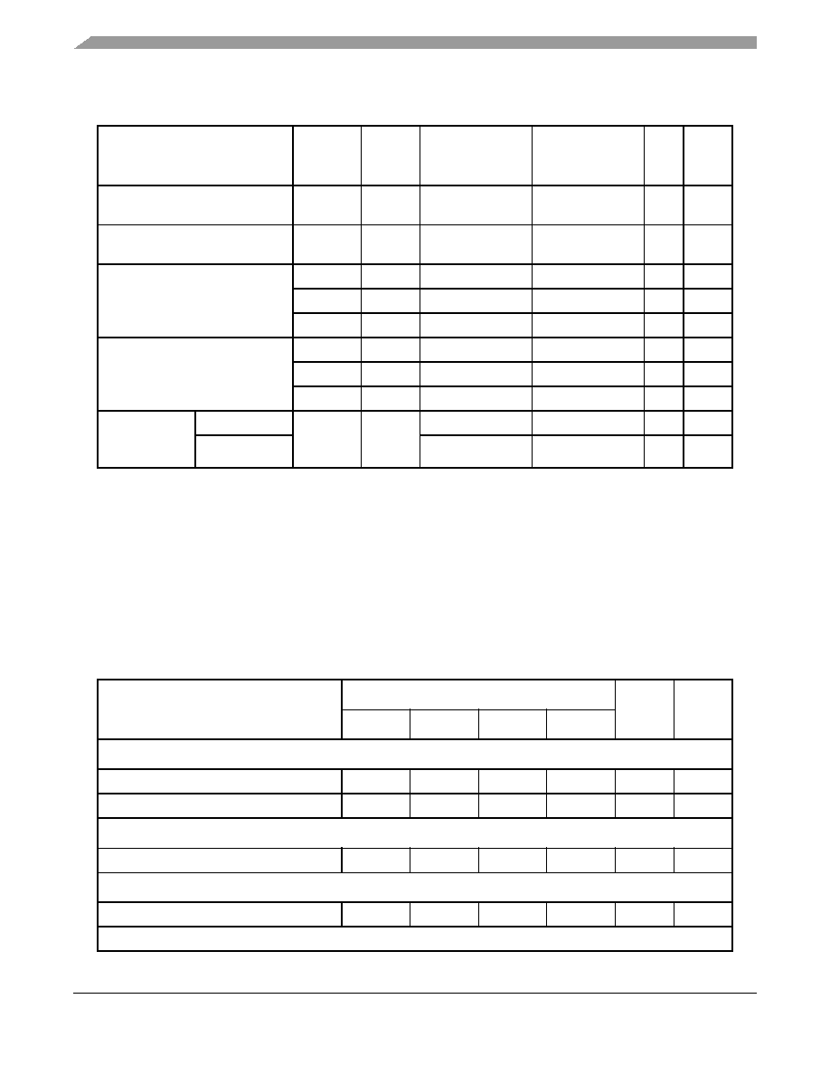
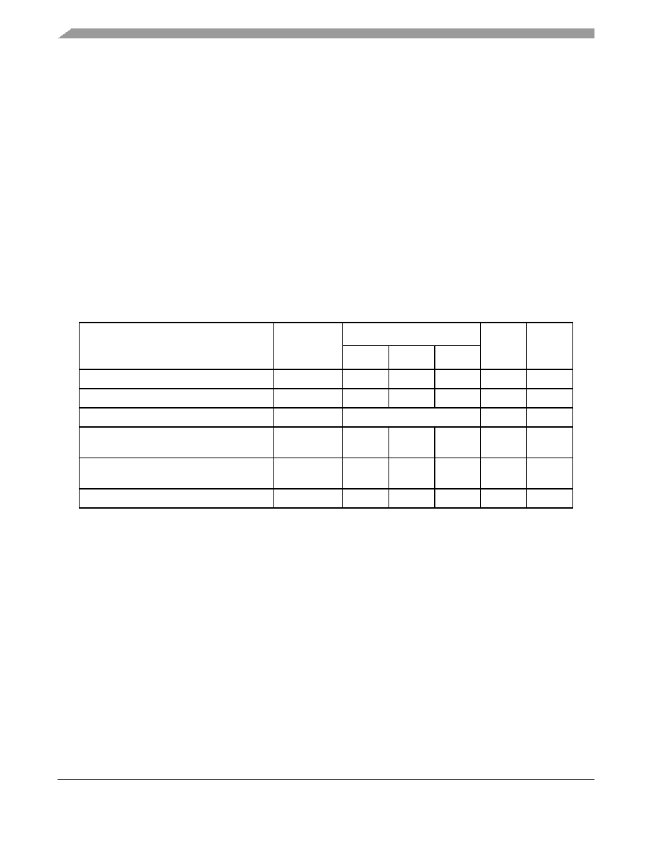
Table 1
compares the key features of the MPC7455 with the key features of the earlier MPC7400, MPC7410,
MPC7450, MPC7451, and MPC7441. To achieve a higher frequency, the number of logic levels per cycle is
reduced. Also, to achieve this higher frequency, the pipeline of the MPC7455 is extended (compared to the
MPC7400), while maintaining the same level of performance as measured by the number of instructions executed
per cycle (IPC).
Table 1. Microarchitecture Comparison
Microarchitectural Specs
MPC7455/MPC7445
MPC7450/MPC7451/
MPC7441
MPC7400/MPC7410
Basic Pipeline Functions
Logic inversions per cycle
18
18
28
Pipeline stages up to execute
5
5
3
Total pipeline stages (minimum)
7
7
4
Pipeline maximum instruction
throughput
3 + Branch
3 + Branch
2 + Branch
Pipeline Resources
Instruction buffer size
12
12
6
Completion buffer size
16
16
8
Renames (integer, float, vector)
16, 16, 16
16, 16, 16
6, 6, 6
Maximum Execution Throughput
SFX
3
3
2
Vector
2 (Any 2 of 4 Units)
2 (Any 2 of 4 Units)
2 (Permute/Fixed)
Scalar floating-point
1
1
1
Out-of-Order Window Size in Execution Queues
SFX integer units
1 Entry
� 3 Queues
1 Entry
� 3 Queues
1 Entry
� 2 Queues
Vector units
In Order, 4 Queues
In Order, 4 Queues
In Order, 2 Queues

MPC7455 RISC Microprocessor Hardware Specifications, Rev. 4.1
8
Freescale Semiconductor
Comparison with the MPC7400, MPC7410, MPC7450, MPC7451, and MPC7441
Scalar floating-point unit
In Order
In Order
In Order
Branch Processing Resources
Prediction structures
BTIC, BHT, Link Stack
BTIC, BHT, Link Stack
BTIC, BHT
BTIC size, associativity
128-Entry, 4-Way
128-Entry, 4-Way
64-Entry, 4-Way
BHT size
2K-Entry
2K-Entry
512-Entry
Link stack depth
8
8
None
Unresolved branches supported
3
3
2
Branch taken penalty (BTIC hit)
1
1
0
Minimum misprediction penalty
6
6
4
Execution Unit Timings (Latency-Throughput)
Aligned load (integer, float, vector)
3-1, 4-1, 3-1
3-1, 4-1, 3-1
2-1, 2-1, 2-1
Misaligned load (integer, float, vector)
4-2, 5-2, 4-2
4-2, 5-2, 4-2
3-2, 3-2, 3-2
L1 miss, L2 hit latency
9 Data/13 Instruction
9 Data/13 Instruction
9 (11)
1
SFX (aDd Sub, Shift, Rot, Cmp, logicals)
1-1
1-1
1-1
Integer multiply (32
� 8, 32 � 16, 32 � 32)
3-1, 3-1, 4-2
3-1, 3-1, 4-2
2-1, 3-2, 5-4
Scalar float
5-1
5-1
3-1
VSFX (vector simple)
1-1
1-1
1-1
VCFX (vector complex)
4-1
4-1
3-1
VFPU (vector float)
4-1
4-1
4-1
VPER (vector permute)
2-1
2-1
1-1
MMUs
TLBs (instruction and data)
128-Entry, 2-Way
128-Entry, 2-Way
128-Entry, 2-Way
Tablewalk mechanism
Hardware + Software
Hardware + Software
Hardware
Instruction BATs/data BATs
8/8
4/4
4/4
L1 I Cache/D Cache Features
Size
32K/32K
32K/32K
32K/32K
Associativity
8-Way
8-Way
8-Way
Locking granularity
Way
Way
Full Cache
Parity on I cache
Word
Word
None
Parity on D cache
Byte
Byte
None
Number of D cache misses (load/store)
5/1
5/1
8 (Any Combination)
Data stream touch engines
4 Streams
4 Streams
4 Streams
On-Chip Cache Features
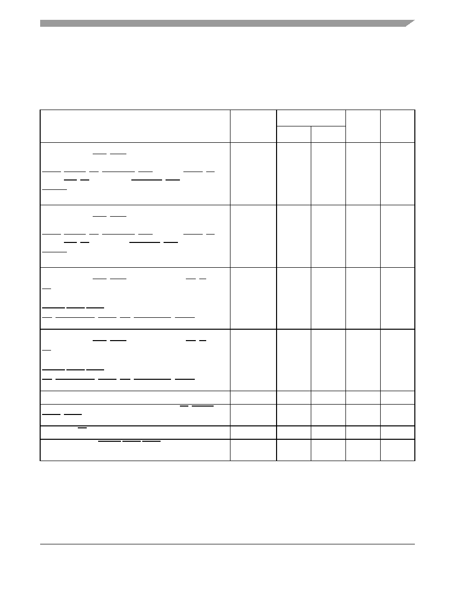
Table 1. Microarchitecture Comparison (continued)
Microarchitectural Specs
MPC7455/MPC7445
MPC7450/MPC7451/
MPC7441
MPC7400/MPC7410

MPC7455 RISC Microprocessor Hardware Specifications, Rev. 4.1
Freescale Semiconductor
9
General Parameters
4
General Parameters
The following list provides a summary of the general parameters of the MPC7455:
Technology
0.18 � m CMOS, six-layer metal
Die size
8.69 mm
� 12.17 mm (106 mm
2
)
Transistor count
33 million
Logic design
Fully-static
Packages
MPC7445: Surface mount 360 ceramic ball grid array (CBGA)
MPC7455: Surface mount 483 ceramic ball grid array (CBGA)
Core power supply
1.3 V � 50 mV DC nominal
I/O power supply
1.8 V � 5% DC, or
2.5 V � 5% DC, or
1.5 V � 5% DC (L3 interface only)
Cache level
L2
L2
L2 tags and controller
only (see off-chip cache
support below)
Size/associativity
256-Kbyte/8-Way
256-Kbyte/8-Way
Access width
256 Bits
256 Bits
Number of 32-byte sectors/line
2
2
Parity
Byte
Byte
Off-Chip Cache Support
2
Cache level
L3
L3
L2
On-chip tag logical size
1MB, 2MB
1MB, 2MB
0.5MB, 1MB, 2MB
Associativity
8-Way
8-Way
2-Way
Number of 32-byte sectors/line
2, 4
2, 4
1, 2, 4
Off-chip data SRAM support
MSUG2 DDR, LW, PB2 MSUG2 DDR, LW, PB2
LW, PB2, PB3
Data path width
64
64
64
Direct mapped SRAM sizes
1 Mbyte, 2 Mbytes
1 Mbyte, 2 Mbytes
0.5 Mbyte, 1 Mbyte,
2 Mbytes
3
Parity
Byte
Byte
Byte
Notes:
1. Numbers in parentheses are for 2:1 SRAM.
2. Not implemented on MPC7445 or MPC7441.
3. Private memory feature not implemented on MPC7400.
Table 1. Microarchitecture Comparison (continued)
Microarchitectural Specs
MPC7455/MPC7445
MPC7450/MPC7451/
MPC7441
MPC7400/MPC7410

MPC7455 RISC Microprocessor Hardware Specifications, Rev. 4.1
10
Freescale Semiconductor
Electrical and Thermal Characteristics
5
Electrical and Thermal Characteristics
This section provides the AC and DC electrical specifications and thermal characteristics for the MPC7455.
5.1 DC Electrical Characteristics
The tables in this section describe the MPC7455 DC electrical characteristics.
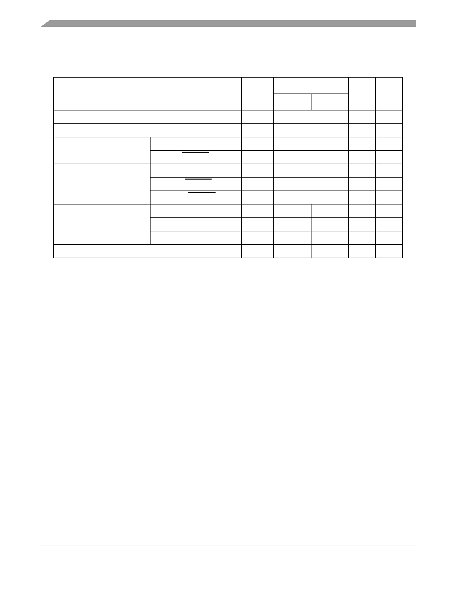
Table 2
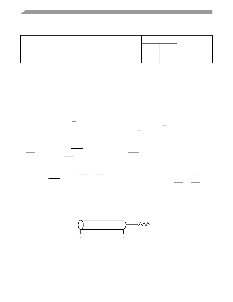
provides the absolute
maximum ratings.
Table 2. Absolute Maximum Ratings
1
Characteristic
Symbol
Maximum Value
Unit
Notes
Core supply voltage
V
DD
�0.3 to 1.95
V
4
PLL supply voltage
AV
DD
�0.3 to 1.95
V
4
Processor bus supply voltage
BVSEL = 0
OV
DD
�0.3 to 1.95
V
3, 6
BVSEL = HRESET or OV
DD
OV
DD
�0.3 to 2.7
V
3, 7
L3 bus supply voltage
L3VSEL = �HRESET
GV
DD
�0.3 to 1.65
V
3, 8
L3VSEL = 0
GV
DD
�0.3 to 1.95
V
3, 9
L3VSEL = HRESET or GV
DD
GV
DD
�0.3 to 2.7
V
3, 10
Input voltage
Processor bus
V
in
�0.3 to OV
DD
+ 0.3
V
2, 5
L3 bus
V
in
�0.3 to GV
DD
+ 0.3
V
2, 5
JTAG signals
V
in
�0.3 to OV
DD
+ 0.3
V
Input voltage
Processor bus
V
in
�0.3 to OV
DD
+ 0.3
V
2, 5
JTAG signals
V
in
�0.3 to OV
DD
+ 0.3
V
Storage temperature range
T
stg
�55 to 150
�C
Notes:
1. Functional and tested operating conditions are given in
Table 4
. Absolute maximum ratings are stress ratings only,
and functional operation at the maximums is not guaranteed. Stresses beyond those listed may affect device
reliability or cause permanent damage to the device.
2. Caution: Vin must not exceed OV
DD
or GV
DD
by more than 0.3 V at any time including during power-on reset.
3. Caution: OV
DD
/GV
DD
must not exceed V
DD
/AV
DD
by more than 2.0 V during normal operation; this limit may be
exceeded for a maximum of 20 ms during power-on reset and power-down sequences.
4. Caution: V
DD
/AV
DD
must not exceed OV
DD
/GV
DD
by more than 1.0 V during normal operation; this limit may be
exceeded for a maximum of 20 ms during power-on reset and power-down sequences.
5. V
in
may overshoot/undershoot to a voltage and for a maximum duration as shown in
Figure 2
.
6. BVSEL must be set to 0, such that the bus is in 1.8 V mode.
7. BVSEL must be set to HRESET or 1, such that the bus is in 2.5 V mode.
8. L3VSEL must be set to �HRESET (inverse of HRESET), such that the bus is in 1.5 V mode.
9. L3VSEL must be set to 0, such that the bus is in 1.8 V mode.
10.L3VSEL must be set to HRESET or 1, such that the bus is in 2.5 V mode.
MPC7455 RISC Microprocessor Hardware Specifications, Rev. 4.1
Freescale Semiconductor
11
Electrical and Thermal Characteristics
Figure 2
shows the undershoot and overshoot voltage on the MPC7455.
Figure 2. Overshoot/Undershoot Voltage
The MPC7455 provides several I/O voltages to support both compatibility with existing systems and migration to
future systems. The MPC7455 core voltage must always be provided at nominal 1.3 V (see
Table 4
for actual
recommended core voltage). Voltage to the L3 I/Os and processor interface I/Os are provided through separate sets
of supply pins and may be provided at the voltages shown in
Table 3
. The input voltage threshold for each bus is
selected by sampling the state of the voltage select pins at the negation of the signal HRESET. The output voltage
will swing from GND to the maximum voltage applied to the OV
DD
or GV
DD
power pins.
Table 3. Input Threshold Voltage Setting
BVSEL Signal
Processor Bus Input
Threshold is Relative to:
L3VSEL Signal
5
L3 Bus Input Threshold is
Relative to:
Notes
0
1.8 V
0
1.8 V
1, 4
�HRESET
Not Available
�HRESET
1.5 V
1, 3
HRESET
2.5 V
HRESET
2.5 V
1, 2
1
2.5 V
1
2.5 V
1
Notes:
1. Caution: The input threshold selection must agree with the OV
DD
/GV
DD
voltages supplied. See notes in
Table 2
.
2. To select the 2.5-V threshold option for the processor bus, BVSEL should be tied to HRESET so that the two signals
change state together. Similarly, to select 2.5 V for the L3 bus, tie L3VSEL to HRESET. This is the preferred method
for selecting this mode of operation.
3. Applicable to L3 bus interface only. �HRESET is the inverse of HRESET.
4. If used, pulldown resistors should be less than 250
.
5. Not implemented on MPC7445.
V
IH
GND
GND � 0.3 V
GND � 0.7 V
Not to Exceed 10%
OV
DD
/GV
DD
+ 20%
V
IL
OV
DD
/GV
DD
OV
DD
/GV
DD
+ 5%
of t
SYSCLK
MPC7455 RISC Microprocessor Hardware Specifications, Rev. 4.1
12
Freescale Semiconductor
Electrical and Thermal Characteristics
Table 4
provides the recommended operating conditions for the MPC7455.
Table 4. Recommended Operating Conditions
1
Characteristic
Symbol
Recommended Value
Unit
Notes
Min
Max
Core supply voltage
V
DD
1.3 V � 50 mV
V
PLL supply voltage
AV
DD
1.3 V � 50 mV
V
2
Processor bus supply voltage
BVSEL = 0
OV
DD
1.8 V � 5%
V
BVSEL = HRESET or OV
DD
OV
DD
2.5 V � 5%
V
L3 bus supply voltage
L3VSEL = 0
GV
DD
1.8 V � 5%
V
L3VSEL = HRESET or GV
DD
GV
DD
2.5 V � 5%
V
L3VSEL = �HRESET
GV
DD
1.5 V � 5%
V
Input voltage
Processor bus
V
in
GND
OV
DD
V
L3 bus
V
in
GND
GV
DD
V
JTAG signals
V
in
GND
OV
DD
V
Die-junction temperature
T
j
0
105
�C
Notes:
1. These are the recommended and tested operating conditions. Proper device operation outside of these conditions
is not guaranteed.
2. This voltage is the input to the filter discussed in
Section 9.2, "PLL Power Supply Filtering,"
and not necessarily the
voltage at the AV
DD
pin which may be reduced from V
DD
by the filter.
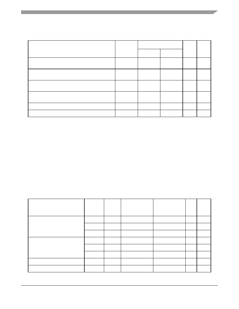
MPC7455 RISC Microprocessor Hardware Specifications, Rev. 4.1
Freescale Semiconductor
13
Electrical and Thermal Characteristics
Table 5
provides the package thermal characteristics for the MPC7455.
Table 6
provides the DC electrical characteristics for the MPC7455.
Table 5. Package Thermal Characteristics
6
Characteristic
Symbol
Value
Unit
Notes
MPC7445 MPC7455
Junction-to-ambient thermal resistance, natural
convection
R
JA
22
20
�C/W
1, 2
Junction-to-ambient thermal resistance, natural
convection, four-layer (2s2p) board
R
JMA
14
14
�C/W
1, 3
Junction-to-ambient thermal resistance, 200 ft/min
airflow, single-layer (1s) board
R
JMA
16
15
�C/W
1, 3
Junction-to-ambient thermal resistance, 200 ft/min
airflow, four-layer (2s2p) board
R
JMA
11
11
�C/W
1, 3
Junction-to-board thermal resistance
R
JB
6
6
�C/W
4
Junction-to-case thermal resistance
R
JC
<0.1
<0.1
�C/W
5
Notes:
1. Junction temperature is a function of on-chip power dissipation, package thermal resistance, mounting site (board)
temperature, ambient temperature, airflow, power dissipation of other components on the board, and board thermal
resistance.
2. Per SEMI G38-87 and JEDEC JESD51-2 with the single-layer board horizontal.
3. Per JEDEC JESD51-6 with the board horizontal.
4. Thermal resistance between the die and the printed-circuit board per JEDEC JESD51-8. Board temperature is
measured on the top surface of the board near the package.
5. Thermal resistance between the die and the case top surface as measured by the cold plate method
(MIL SPEC-883 Method 1012.1) with the calculated case temperature. The actual value of R
JC
for the part is less
than 0.1�C/W.
6. Refer to
Section 9.8, "Thermal Management Information,"
for more details about thermal management.
Table 6. DC Electrical Specifications
At recommended operating conditions. See
Table 4
.
Characteristic
Nominal
Bus
Voltage
1
Symbol
Min
Max
Unit
Notes
Input high voltage
(all inputs except SYSCLK)
1.5
V
IH
GV
DD
� 0.65
GV
DD
+ 0.3
V
6
1.8
V
IH
OV
DD
/GV
DD
� 0.65 OV
DD
/GV
DD
+ 0.3
V
2.5
V
IH
1.7
OV
DD
/GV
DD
+ 0.3
V
Input low voltage
(all inputs except SYSCLK)
1.5
V
IL
�0.3
GV
DD
� 0.35
V
6
1.8
V
IL
�0.3
OV
DD
/GV
DD
� 0.35
V
2.5
V
IL
�0.3
0.7
V
SYSCLK input high voltage
--
CV
IH
1.4
OV
DD
+ 0.3
V
SYSCLK input low voltage
--
CV
IL
�0.3
0.4
V
MPC7455 RISC Microprocessor Hardware Specifications, Rev. 4.1
14
Freescale Semiconductor
Electrical and Thermal Characteristics
Table 7
provides the power consumption for the MPC7455.
Input leakage current,
V
in
= GV
DD
/OV
DD
+ 0.3 V
--
I
in
--
30
�A
2, 3
High impedance (off-state) leakage
current, V
in
= GV
DD
/OV
DD
+ 0.3 V
--
I
TSI
--
30
�A
2, 3, 5
Output high voltage, I
OH
= �5 mA
1.5
V
OH
GV
DD
� 0.45
--
V
6
1.8
V
OH
OV
DD
/GV
DD
� 0.45
--
V
2.5
V
OH
1.7
--
V
Output low voltage, I
OL
= 5 mA
1.5
V
OL
--
0.45
V
6
1.8
V
OL
--
0.45
V
2.5
V
OL
--
0.7
V
Capacitance,
V
in
= 0 V,
f = 1 MHz
L3 interface
--
C
in
--
9.5
pF
4
All other inputs
--
8.0
pF
4
Notes:
1. Nominal voltages; see
Table 4
for recommended operating conditions.
2. For processor bus signals, the reference is OV
DD
while GV
DD
is the reference for the L3 bus signals.
3. Excludes test signals and IEEE 1149.1 boundary scan (JTAG) signals.
4. Capacitance is periodically sampled rather than 100% tested.
5. The leakage is measured for nominal OV
DD
/GV
DD
and V
DD
, or both OV
DD
/GV
DD
and V
DD
must vary in the same
direction (for example, both OV
DD
and V
DD
vary by either +5% or �5%).
6. Applicable to L3 bus interface only.
Table 7. Power Consumption for MPC7455
Processor (CPU) Frequency
Unit
Notes
733 MHz
867 MHz
933 MHz
1 GHz
Full-Power Mode
Typical 11.5
12.9
13.6
15.0
W
1,
3
Maximum 17.0
19.0
20.0
22.0
W
1,
2
Doze Mode
Typical
--
--
--
--
W
4
Nap Mode
Typical
8.0
8.0
8.0
8.0
W
1, 3
Sleep Mode
Table 6. DC Electrical Specifications (continued)
At recommended operating conditions. See
Table 4
.
Characteristic
Nominal
Bus
Voltage
1
Symbol
Min
Max
Unit
Notes

MPC7455 RISC Microprocessor Hardware Specifications, Rev. 4.1
Freescale Semiconductor
15
Electrical and Thermal Characteristics
5.2 AC Electrical Characteristics
This section provides the AC electrical characteristics for the MPC7455. After fabrication, functional parts are
sorted by maximum processor core frequency as shown in
Section 5.2.1, "Clock AC Specifications
,"
and tested for
conformance to the AC specifications for that frequency. The processor core frequency is determined by the bus
(SYSCLK) frequency and the settings of the PLL_CFG[0:4] signals. Parts are sold by maximum processor core
frequency; see
Section 11, "Ordering Information.
"
5.2.1 Clock AC Specifications
Table 8
provides the clock AC timing specifications as defined in
Figure 3
.
Typical
7.6
7.6
7.6
7.6
W
1, 3
Deep Sleep Mode (PLL Disabled)
Typical
7.3
7.3
7.3
7.3
W
1, 3
Notes:
1. These values apply for all valid processor bus and L3 bus ratios. The values do not include I/O supply power (OV
DD
and GV
DD
) or PLL supply power (AV
DD
). OV
DD
and GV
DD
power is system dependent, but is typically <5% of V
DD
power. Worst case power consumption for AV
DD
< 3 mW.
2. Maximum power is measured at nominal V
DD
(see
Table 4
) while running an entirely cache-resident, contrived
sequence of instructions which keep the execution units, with or without AltiVec, maximally busy.
3. Typical power is an average value measured at the nominal recommended V
DD
(see
Table 4
) and 65
�C in a system
while running a typical code sequence.
4. Doze mode is not a user-definable state; it is an intermediate state between full-power and either nap or sleep mode.
As a result, power consumption for this mode is not tested.
Table 8. Clock AC Timing Specifications
At recommended operating conditions. See
Table 4
.
Characteristic
Symbol
Maximum Processor Core Frequency
Unit
Notes
733 MHz
867 MHz
933 MHz
1 GHz
Min
Max
Min
Max
Min
Max
Min
Max
Processor frequency
f
core
500
733
500
867
500
933
500
1000
MHz
1
VCO frequency
f
VCO
1000
1466
1000
1734
1000
1866
1000
2000
MHz
1
SYSCLK frequency
f
SYSCLK
33
133
33
133
33
133
33
133
MHz
1
SYSCLK cycle time
t
SYSCLK
7.5
30
7.5
30
7.5
30
7.5
30
ns
SYSCLK rise and fall time
t
KR
, t
KF
--
1.0
--
1.0
--
1.0
--
1.0
ns
2
SYSCLK duty cycle
measured at OV
DD
/2
t
KHKL
/
t
SYSCLK
40
60
40
60
40
60
40
60
%
3
Table 7. Power Consumption for MPC7455 (continued)
Processor (CPU) Frequency
Unit
Notes
733 MHz
867 MHz
933 MHz
1 GHz

MPC7455 RISC Microprocessor Hardware Specifications, Rev. 4.1
16
Freescale Semiconductor
Electrical and Thermal Characteristics
Figure 3
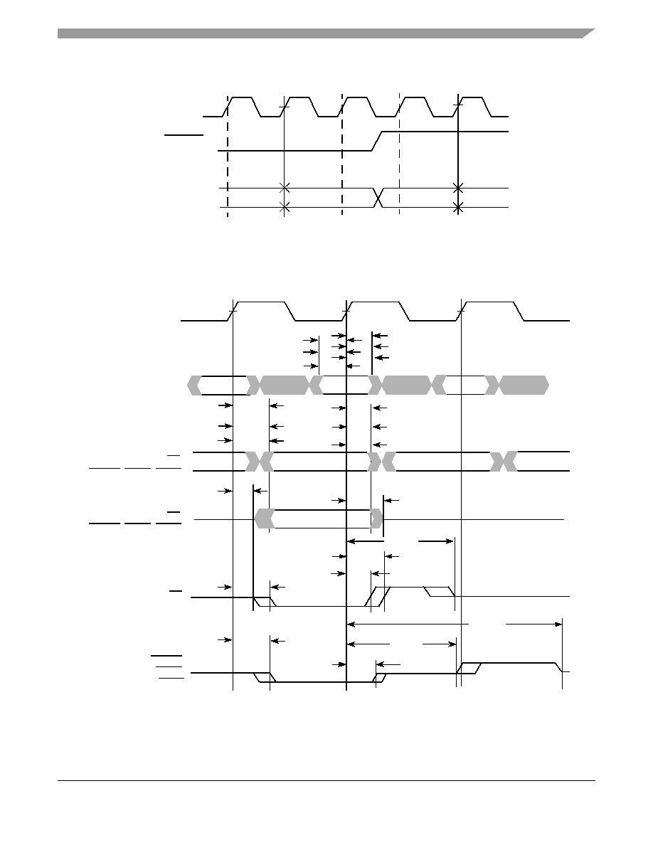
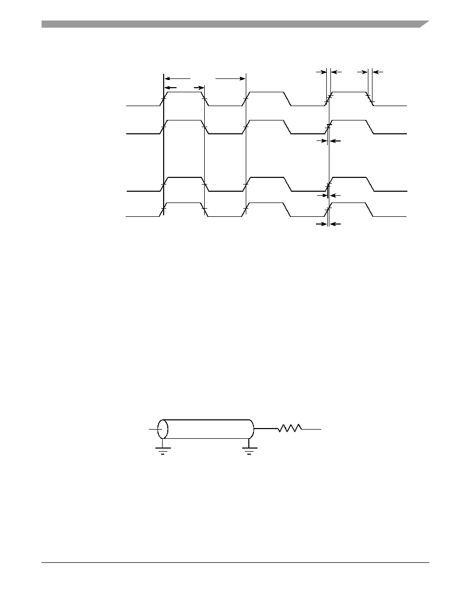
provides the SYSCLK input timing diagram.
Figure 3. SYSCLK Input Timing Diagram
SYSCLK jitter
--
� 150
--
� 150
--
� 150
--
� 150
ps
4, 6
Internal PLL relock time
--
100
--
100
--
100
--
100
�s
5
Notes:
1. Caution: The SYSCLK frequency and PLL_CFG[0:4] settings must be chosen such that the resulting SYSCLK
(bus) frequency, CPU (core) frequency, and PLL (VCO) frequency do not exceed their respective maximum or
minimum operating frequencies. Refer to the PLL_CFG[0:4] signal description in
Section 9.1, "PLL Configuration,"
for valid PLL_CFG[0:4] settings.
2. Rise and fall times for the SYSCLK input measured from 0.4 to 1.4 V.
3. Timing is guaranteed by design and characterization.
4. This represents total input jitter--short term and long term combined--and is guaranteed by design.
5. Relock timing is guaranteed by design and characterization. PLL-relock time is the maximum amount of time
required for PLL lock after a stable V
DD
and SYSCLK are reached during the power-on reset sequence. This
specification also applies when the PLL has been disabled and subsequently re-enabled during sleep mode. Also
note that HRESET must be held asserted for a minimum of 255 bus clocks after the PLL-relock time during the
power-on reset sequence.
6. The SYSCLK driver's closed loop jitter bandwidth should be <500 kHz at �20 dB. The bandwidth must be set low
to allow cascade connected PLL-based devices to track SYSCLK drivers with the specified jitter.
Table 8. Clock AC Timing Specifications (continued)
At recommended operating conditions. See
Table 4
.
Characteristic
Symbol
Maximum Processor Core Frequency
Unit
Notes
733 MHz
867 MHz
933 MHz
1 GHz
Min
Max
Min
Max
Min
Max
Min
Max
SYSCLK
VM
VM
VM
CV
IH
CV
IL
VM = Midpoint Voltage (OV
DD
/2)
t
SYSCLK
t
KR
t
KF
t
KHKL
MPC7455 RISC Microprocessor Hardware Specifications, Rev. 4.1
Freescale Semiconductor
17
Electrical and Thermal Characteristics
5.2.2 Processor Bus AC Specifications
Table 9
provides the processor bus AC timing specifications for the MPC7455 as defined in
Figure 4
and
Figure 5
.
Timing specifications for the L3 bus are provided in
Section 5.2.3, "L3 Clock AC Specifications
."
Table 9. Processor Bus AC Timing Specifications
1
At recommended operating conditions. See
Table 4
.
Parameter
Symbol
2
All Speed Grades
Unit
Notes
Min
Max
Input setup times:
A[0:35], AP[0:4], GBL, TBST, TSIZ[0:2], TT[0:3], D[0:63],
DP[0:7]
AACK, ARTRY, BG, CKSTP_IN, DBG, DTI[0:3], QACK, TA,
TBEN, TEA, TS, EXT_QUAL, PMON_IN, SHD[0:1]
BMODE[0:1], BVSEL, L3VSEL
t
AVKH
t
IVKH
t
MVKH
2.0
2.0
2.0
--
--
--
ns
8
Input hold times:
A[0:35], AP[0:4], GBL, TBST, TSIZ[0:2], TT[0:3], D[0:63],
DP[0:7]
AACK, ARTRY, BG, CKSTP_IN, DBG, DTI[0:3], QACK, TA,
TBEN, TEA, TS,EXT_QUAL, PMON_IN, SHD[0:1]
BMODE[0:1], BVSEL, L3VSEL
t
AXKH
t
IXKH
t
MXKH
0
0
0
--
--
--
ns
8
Output valid times:
A[0:35], AP[0:4], GBL, TBST, TSIZ[0:2], TT[0:3], WT, CI
TS
D[0:63], DP[0:7]
ARTRY/SHD0/SHD1
BR, CKSTP_OUT, DRDY, HIT, PMON_OUT, QREQ]
t
KHAV
t
KHTSV
t
KHDV
t
KHARV
t
KHOV
--
--
--
--
--
2.5
2.5
2.5
2.5
2.5
ns
Output hold times:
A[0:35], AP[0:4], GBL, TBST, TSIZ[0:2], TT[0:3], WT, CI
TS
D[0:63], DP[0:7]
ARTRY/SHD0/SHD1
BR, CKSTP_OUT, DRDY, HIT, PMON_OUT, QREQ
t
KHAX
t
KHTSX
t
KHDX
t
KHARX
t
KHOX
0.5
0.5
0.5
0.5
0.5
--
--
--
--
--
ns
SYSCLK to output enable
t
KHOE
0.5
--
ns
SYSCLK to output high impedance (all except TS, ARTRY,
SHD0, SHD1)
t
KHOZ
--
3.5
ns
SYSCLK to TS high impedance after precharge
t
KHTSPZ
--
1
t
SYSCLK
3, 4, 5
Maximum delay to ARTRY/SHD0/SHD1 precharge
t
KHARP
--
1
t
SYSCLK
3, 5,
6, 7
MPC7455 RISC Microprocessor Hardware Specifications, Rev. 4.1
18
Freescale Semiconductor
Electrical and Thermal Characteristics
Figure 4
provides the AC test load for the MPC7455.
Figure 4. AC Test Load
SYSCLK to ARTRY/SHD0/SHD1 high impedance after
precharge
t
KHARPZ
--
2
t
SYSCLK
3, 5,
6, 7
Notes:
1. All input specifications are measured from the midpoint of the signal in question to the midpoint of the rising edge of the input
SYSCLK. All output specifications are measured from the midpoint of the rising edge of SYSCLK to the midpoint of the signal
in question. All output timings assume a purely resistive 50-
load (see
Figure 4
). Input and output timings are measured at
the pin; time-of-flight delays must be added for trace lengths, vias, and connectors in the system.
2. The symbology used for timing specifications herein follows the pattern of t
(signal)(state)(reference)(state)
for inputs and
t
(reference)(state)(signal)(state)
for outputs. For example, t
IVKH
symbolizes the time input signals (I) reach the valid state (V)
relative to the SYSCLK reference (K) going to the high (H) state or input setup time. And t
KHOV
symbolizes the time from
SYSCLK(K) going high (H) until outputs (O) are valid (V) or output valid time. Input hold time can be read as the time that the
input signal (I) went invalid (X) with respect to the rising clock edge (KH) (note the position of the reference and its state for
inputs) and output hold time can be read as the time from the rising edge (KH) until the output went invalid (OX).
3. t
sysclk
is the period of the external clock (SYSCLK) in ns. The numbers given in the table must be multiplied by the period of
SYSCLK to compute the actual time duration (in ns) of the parameter in question.
4. According to the bus protocol, TS is driven only by the currently active bus master. It is asserted low then precharged high
before returning to high impedance as shown in
Figure 6
. The nominal precharge width for TS is 0.5
� t
SYSCLK
, that is, less
than the minimum t
SYSCLK
period, to ensure that another master asserting TS on the following clock will not contend with the
precharge. Output valid and output hold timing is tested for the signal asserted. Output valid time is tested for precharge. The
high-impedance behavior is guaranteed by design.
5. Guaranteed by design and not tested.
6. According to the bus protocol, ARTRY can be driven by multiple bus masters through the clock period immediately following
AACK. Bus contention is not an issue because any master asserting ARTRY will be driving it low. Any master asserting it low
in the first clock following AACK will then go to high impedance for one clock before precharging it high during the second
cycle after the assertion of AACK. The nominal precharge width for ARTRY is 1.0 t
SYSCLK
; that is, it should be high
impedance as shown in
Figure 6
before the first opportunity for another master to assert ARTRY. Output valid and output
hold timing is tested for the signal asserted. The high-impedance behavior is guaranteed by design.
7. According to the MPX bus protocol, SHD0 and SHD1 can be driven by multiple bus masters beginning the cycle of TS. Timing
is the same as ARTRY, that is, the signal is high impedance for a fraction of a cycle, then negated for up to an entire cycle
(crossing a bus cycle boundary) before being three-stated again. The nominal precharge width for SHD0 and SHD1 is 1.0
t
SYSCLK
. The edges of the precharge vary depending on the programmed ratio of core-to-bus (PLL configurations).
8. BMODE[0:1] and BVSEL are mode select inputs and are sampled before and after HRESET negation. These paramenters
represent the input setup and hold times for each sample. These values are guaranteed by design and not tested. These
inputs must remain stable after the second sample. See
Figure 5
for sample timing.
Table 9. Processor Bus AC Timing Specifications
1
(continued)
At recommended operating conditions. See
Table 4
.
Parameter
Symbol
2
All Speed Grades
Unit
Notes
Min
Max
Output
Z
0
= 50
OV
DD
/2
R
L
= 50
MPC7455 RISC Microprocessor Hardware Specifications, Rev. 4.1
Freescale Semiconductor
19
Electrical and Thermal Characteristics
Figure 5
provides the mode select input timing diagram for the MPC7455.
Figure 5. Mode Input Timing Diagram
Figure 6
provides the input/output timing diagram for the MPC7455.
Figure 6. Input/Output Timing Diagram
HRESET
Mode Signals
VM = Midpoint Voltage (OVDD/2)
SYSCLK
Firs t Sample
Second Sample
VM
VM
SYSCLK
All Inputs
VM
VM = Midpoint Voltage (OV
DD
/2)
All Outputs
t
KHOX
VM
t
KHDV
(Except TS,
ARTRY
,
SHD0, SHD1)
All Outputs
TS
ARTRY,
(Except TS,
ARTRY
,
SHD0, SHD1)
VM
t
KHOE
t
KHOZ
t
KHTSPZ
t
KHARPZ
t
KHARP
SHD1
SHD0,
t
KHOV
t
KHAV
t
KHDX
t
KHAX
t
IXKH
t
AXKH
t
KHTSX
t
KHTSV
t
KHTSV
t
KHARV
t
KHARX
t
IVKH
t
AVKH
t
MVKH
t
MXKH
MPC7455 RISC Microprocessor Hardware Specifications, Rev. 4.1
20
Freescale Semiconductor
Electrical and Thermal Characteristics
5.2.3 L3 Clock AC Specifications
The L3_CLK frequency is programmed by the L3 configuration register (L3CR[6:8]) core-to-L3 divisor ratio. See
Table 18
for example core and L3 frequencies at various divisors.
Table 10
provides the potential range of L3_CLK
output AC timing specifications as defined in
Figure 7
.
The maximum L3_CLK frequency is the core frequency divided by two. Given the high core frequencies available
in the MPC7455, however, most SRAM designs will be not be able to operate in this mode using current technology
and, as a result, will select a greater core-to-L3 divisor to provide a longer L3_CLK period for read and write access
to the L3 SRAMs. Therefore, the typical L3_CLK frequency shown in
Table 10
is considered to be the practical
maximum in a typical system. The maximum L3_CLK frequency for any application of the MPC7455 will be a
function of the AC timings of the MPC7455, the AC timings for the SRAM, bus loading, and printed-circuit board
trace length, and may be greater or less than the value given in
Table 10
.
Freescale is similarly limited by system constraints and cannot perform tests of the L3 interface on a socketed part
on a functional tester at the maximum frequencies of
Table 10
. Therefore, functional operation and AC timing
information are tested at core-to-L3 divisors which result in L3 frequencies at 200 MHz or less.
Table 10. L3_CLK Output AC Timing Specifications
At recommended operating conditions. See
Table 4
.
Parameter
Symbol
All Speed Grades
Unit
Notes
Min
Typ
Max
L3 clock frequency
f
L3_CLK
75
250
--
MHz
1
L3 clock cycle time
t
L3_CLK
--
4.0
13.3
ns
L3 clock duty cycle
t
CHCL
/t
L3_CLK
50
%
2
L3 clock output-to-output skew (L1_CLK0 to
L1_CLK1)
t
L3CSKW1
--
--
200
ps
3
L3 clock output-to-output skew (L1_CLK[0:1]
to L1_ECHO_CLK[2:3])
t
L3CSKW2
--
--
100
ps
4
L3 clock jitter
--
--
�50
ps
5
Notes:
1. The maximum L3 clock frequency will be system dependent. See
Section 5.2.3, "L3 Clock AC Specifications,"
for
an explanation that this maximum frequency is not functionally tested at speed by Freescale.
2. The nominal duty cycle of the L3 output clocks is 50% measured at midpoint voltage.
3. Maximum possible skew between L3_CLK0 and L3_CLK1. This parameter is critical to the address and control
signals which are common to both SRAM chips in the L3.
4. Maximum possible skew between L3_CLK0 and L3_ECHO_CLK1 or between L3_CLK1 and L3_ECHO_CLK3 for
PB2 or late write SRAM. This parameter is critical to the write data signals which are separately latched onto each
SRAM part by these pairs of signals.
5. Guaranteed by design and not tested. The input jitter on SYSCLK affects L3 output clocks and the L3
address/data/control signals equally and, therefore, is already comprehended in the AC timing and does not have
to be considered in the L3 timing analysis. The clock-to-clock jitter shown here is uncertainty in the internal clock
period caused by supply voltage noise or thermal effects. This must be accounted for, along with clock skew, in
any L3 timing analysis.
MPC7455 RISC Microprocessor Hardware Specifications, Rev. 4.1
Freescale Semiconductor
21
Electrical and Thermal Characteristics
The L3_CLK timing diagram is shown in
Figure 7
.
Figure 7. L3_CLK_OUT Output Timing Diagram
5.2.4 L3 Bus AC Specifications
The MPC7455 L3 interface supports three different types of SRAM: source-synchronous, double data rate (DDR)
MSUG2 SRAM, late write SRAMs, and pipeline burst (PB2) SRAMs. Each requires a different protocol on the L3
interface and a different routing of the L3 clock signals. The type of SRAM is programmed in L3CR[22:23] and the
MPC7455 then follows the appropriate protocol for that type. The designer must connect and route the L3 signals
appropriately for each type of SRAM. Following are some observations about the chip-to-SRAM interface.
�
The routing for the point-to-point signals (L3_CLK[0:1], L3DATA[0:63], L3DP[0:7], and
L3_ECHO_CLK[0:3]) to a particular SRAM should be delay matched. If necessary, the length of traces can
be altered in order to intentionally skew the timing and provide additional setup or hold time margin.
�
For a 1-Mbyte L3, use address bits 16:0 (bit 0 is LSB).
�
No pull-up resistors are required for the L3 interface.
�
For high speed operations, L3 interface address and control signals should be a `T' with minimal stubs to
the two loads; data and clock signals should be point-to-point to their single load.
Figure 8
shows the AC
test load for the L3 interface.
Figure 8. AC Test Load for the L3 Interface
In general, if routing is short, delay-matched, and designed for incident wave reception and minimal reflection, there
is a high probability that the AC timing of the MPC7455 L3 interface will meet the maximum frequency operation
of appropriately chosen SRAMs. This is despite the pessimistic, guard-banded AC specifications (see
Table 12
,
Table 13
, and
Table 14
), the limitations of functional testers described in
Section 5.2.3, "L3 Clock AC
Specifications
,"
and the uncertainty of clocks and signals which inevitably make worst-case critical path timing
analysis pessimistic.
L3_CLK0
VM
t
L3CR
t
L3CF
VM
VM
VM
L3_CLK1
VM
VM
t
L3_CLK
t
CHCL
VM
t
L3CSKW1
L3_ECHO_CLK1
L3_ECHO_CLK3
VM
VM
VM
VM
t
L3CSKW2
VM
VM
VM
VM
t
L3CSKW2
For PB2 or Late Write:
Output
Z
0
= 50
GV
DD
/2
R
L
= 50

MPC7455 RISC Microprocessor Hardware Specifications, Rev. 4.1
22
Freescale Semiconductor
Electrical and Thermal Characteristics
More specifically, certain signals within groups should be delay-matched with others in the same group while
intergroup routing is less critical. Only the address and control signals are common to both SRAMs and additional
timing margin is available for these signals. The double-clocked data signals are grouped with individual clocks as
shown in
Figure 9
or
Figure 11
, depending on the type of SRAM. For example, for the MSUG2 DDR SRAM (see
Figure 9
); L3DATA[0:31], L3DP[0:3], and L3_CLK[0] form a closely coupled group of outputs from the MPC7455;
while L3DATA[0:15], L3DP[0:1], and L3_ECHO_CLK[0] form a closely coupled group of inputs.
The MPC7450 RISC Microprocessor Family User's Manual refers to logical settings called `sample points' used in
the synchronization of reads from the receive FIFO. The computation of the correct value for this setting is
system-dependent and is described in the MPC7450 RISC Microprocessor Family User's Manual. Three
specifications are used in this calculation and are given in
Table 11
. It is essential that all three specifications are
included in the calculations to determine the sample points, as incorrect settings can result in errors and
unpredictable behavior. For more information, see the MPC7450 RISC Microprocessor Family User's Manual.
5.2.4.1 L3 Bus AC Specifications for DDR MSUG2 SRAMs
When using DDR MSUG2 SRAMs at the L3 interface, the parts should be connected as shown in
Figure 9
.
Outputs from the MPC7455 are actually launched on the edges of an internal clock phase-aligned to SYSCLK
(adjusted for core and L3 frequency divisors). L3_CLK0 and L3_CLK1 are this internal clock output with 90� phase
delay, so outputs are shown synchronous to L3_CLK0 and L3_CLK1. Output valid times are typically negative
when referenced to L3_CLKn because the data is launched one-quarter period before L3_CLKn to provide adequate
setup time at the SRAM after the delay-matched address, control, data, and L3_CLKn signals have propagated
across the printed-wiring board.
Inputs to the MPC7455 are source-synchronous with the CQ clock generated by the DDR MSUG2 SRAMs. These
CQ clocks are received on the L3_ECHO_CLKn inputs of the MPC7455. An internal circuit delays the incoming
L3_ECHO_CLKn signal such that it is positioned within the valid data window at the internal receiving latches. This
delayed clock is used to capture the data into these latches which comprise the receive FIFO. This clock is
asynchronous to all other processor clocks. This latched data is subsequently read out of the FIFO synchronously to
the processor clock. The time between writing and reading the data is set by the using the sample point settings
defined in the L3CR register.
Table 11. Sample Points Calculation Parameters
Parameter
Symbol
Max
Unit
Notes
Delay from processor clock to internal_L3_CLK
t
AC
3/4
t
L3_CLK
1
Delay from internal_L3_CLK to L3_CLK
n output pins
t
CO
3
ns
2
Delay from L3_ECHO_CLK
n to receive latch
t
ECI
3
ns
3
Notes:
1. This specification describes a logical offset between the internal clock edge used to launch the L3 address and
control signals (this clock edge is phase-aligned with the processor clock edge) and the internal clock edge used to
launch the L3_CLK
n signals. With proper board routing, this offset ensures that the L3_CLKn edge will arrive at the
SRAM within a valid address window and provide adequate setup and hold time. This offset is reflected in the L3
bus interface AC timing specifications, but must also be separately accounted for in the calculation of sample points
and, thus, is specified here.
2. This specification is the delay from a rising or falling edge on the internal_L3_CLK signal to the corresponding rising
or falling edge at the L3CLK
n pins.
3. This specification is the delay from a rising or falling edge of L3_ECHO_CLK
n to data valid and ready to be sampled
from the FIFO.

MPC7455 RISC Microprocessor Hardware Specifications, Rev. 4.1
Freescale Semiconductor
23
Electrical and Thermal Characteristics
Table 12
provides the L3 bus interface AC timing specifications for the configuration as shown in
Figure 9
,
assuming the timing relationships shown in
Figure 10
and the loading shown in
Figure 8
.
Table 12. L3 Bus Interface AC Timing Specifications for MSUG2
At recommended operating conditions. See
Table 4
.
Parameter
Symbol
All Speed Grades
8
Unit
Notes
L3OH0 = 0, L3OH1 = 0 L3OH0 = 0, L3OH1 =1 L3OH0 = 1, L3OH1 = 0 L3OH0 = 1, L3OH1 = 1
Min
Max
Min
Max
Min
Max
Min
Max
L3_CLK rise
and fall time
t
L3CR
,
t
L3CF
--
1.0
--
1.0
--
1.0
--
1.0
ns
1
Setup times:
Data and
parity
t
L3DVEH
,
t
L3DVEL
� 0.1
--
� 0.1
--
� 0.1
--
� 0.1
--
ns
2, 3,
4
Input hold
times: Data
and parity
t
L3DXEH
,
t
L3DXEL
t
L3_CLK
/4
+ 0.30
--
t
L3_CLK
/4
+ 0.30
--
t
L3_CLK
/4
+ 0.30
--
t
L3_CLK
/4
+ 0.30
--
ns
2, 4
Valid times:
Data and
parity
t
L3CHDV
,
t
L3CLDV
--
(� t
L3_CLK
/4)
+ 0.60
--
(� t
L3_CLK
/4)
+ 0.40
--
(� t
L3_CLK
/4)
+ 0.20
--
(� t
L3_CLK
/4)
+ 0.00
ns
5, 6,
7
Valid times:
All other
outputs
t
L3CHOV
--
t
L3_CLK
/4
+ 0.80
--
t
L3_CLK
/4
+ 0.60
--
t
L3_CLK
/4
+ 0.40
--
t
L3_CLK
/4
+ 0.20
ns
5, 7
Output hold
times: Data
and parity
t
L3CHDX
,
t
L3CLDX,
t
L3_CLK
/4
� 0.40
--
t
L3_CLK
/4
� 0.60
--
t
L3_CLK
/4
� 0.80
--
t
L3_CLK
/4
� 1.00
--
ns
5, 6,
7
Output hold
times: All
other outputs
t
L3CHOX
t
L3_CLK
/4
� 0.20
--
t
L3_CLK
/4
� 0.40
--
t
L3_CLK
/4
� 0.60
--
t
L3_CLK
/4
� 0.80
--
ns
5, 7
L3_CLK to
high
impedance:
Data and
parity
t
L3CLDZ
--
t
L3_CLK
/2
--
t
L3_CLK
/2
--
t
L3_CLK
/2
--
t
L3_CLK
/2
ns

MPC7455 RISC Microprocessor Hardware Specifications, Rev. 4.1
24
Freescale Semiconductor
Electrical and Thermal Characteristics
L3_CLK to
high
impedance:
All other
outputs
t
L3CHOZ
--
t
L3_CLK
/4
+ 2.0
--
t
L3_CLK
/4
+ 2.0
t
L3_CLK
/4
+ 2.0
--
t
L3_CLK
/4
+ 2.0
--
ns
Notes:
1. Rise and fall times for the L3_CLK output are measured from 20% to 80% of GV
DD
.
2. For DDR, all input specifications are measured from the midpoint of the signal in question to the midpoint voltage of the rising
or falling edge of the input L3_ECHO_CLK
n (see
Figure 10
). Input timings are measured at the pins.
3. For DDR, the input data will typically follow the edge of L3_ECHO_CLK
n as shown in
Figure 10
. For consistency with other
input setup time specifications, this will be treated as negative input setup time.
4. t
L3_CLK
/4 is one-fourth the period of L3_CLK
n. This parameter indicates that the MPC7455 can latch an input signal that is
valid for only a short time before and a short time after the midpoint between the rising and falling (or falling and rising) edges
of L3_ECHO_CLK
n at any frequency.
5. All output specifications are measured from the midpoint voltage of the rising (or for DDR write data, also the falling) edge
of L3_CLK to the midpoint of the signal in question. The output timings are measured at the pins. All output timings assume
a purely resistive 50-
load (see
Figure 8
).
6. For DDR, the output data will typically lead the edge of L3_CLK
n as shown in
Figure 10
. For consistency with other output
valid time specifications, this will be treated as negative output valid time.
7. t
L3_CLK
/4 is one-fourth the period of L3_CLK
n. This parameter indicates that the specified output signal is actually launched
by an internal clock delayed in phase by 90�. Therefore, there is a frequency component to the output valid and output hold
times such that the specified output signal will be valid for approximately one L3_CLK period starting three-fourths of a clock
prior to the edge on which the SRAM will sample it and ending one-fourth of a clock period after the edge it will be sampled.
8. These configuration bits allow the AC timing of the L3 interface to be altered via software. L3OH0 = L2CR[12],
L30H1 = L3CR[12]. Revisions of the MPC7455 not described by this document may implement these bits differently. See
Section 11.1, "Part Numbers Fully Addressed by This Document,"
and
Section 11.2, "Part Numbers Not Fully Addressed by
This Document,"
for more information on which devices are addressed by this document.
Table 12. L3 Bus Interface AC Timing Specifications for MSUG2 (continued)
At recommended operating conditions. See
Table 4
.
Parameter
Symbol
All Speed Grades
8
Unit
Notes
L3OH0 = 0, L3OH1 = 0 L3OH0 = 0, L3OH1 =1 L3OH0 = 1, L3OH1 = 0 L3OH0 = 1, L3OH1 = 1
Min
Max
Min
Max
Min
Max
Min
Max
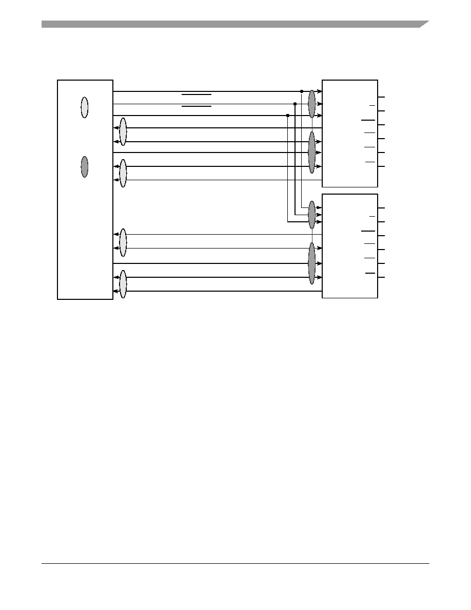
MPC7455 RISC Microprocessor Hardware Specifications, Rev. 4.1
Freescale Semiconductor
25
Electrical and Thermal Characteristics
Figure 9
shows the typical connection diagram for the MPC7455 interfaced to MSUG2 SRAMs such as the
Freescale MCM64E836.
Figure 9. Typical Source Synchronous 2-Mbyte L3 Cache DDR Interface
Denotes
Receive (SRAM
to MPC7455)
Aligned Signals
{L3DATA[0:15],
{L3DATA[16:31],
{L3_DATA[32:47],
L3ADDR[17:0]
L3_CNTL[0]
L3_CLK[0]
L3_CLK[1]
L3_ECHO_CLK[0]
L3_ECHO_CLK[1]
L3ECHO_CLK[2]
L3_ECHO_CLK[3]
{L3DATA[48:63],
L3DP[0:1]}
L3DP[2:3]}
L3DP[4:5]}
L3DP[6:7]}
CQ
SA[17:0]
CK
B1
B2
SRAM 0
SRAM 1
CQ
D[0:17]
D[18:35]
CQ
SA[17:0]
CK
B1
B2
CQ
D[0:17]
D[18:35]
L3_CNTL[1]
NC
NC
GND
GND
GND
NC
NC
GND
GND
GND
MPC7455
Denotes
Receive (SRAM
to MPC7455)
Aligned Signals
Denotes
Transmit
(MPC7455 to
SRAM)
Aligned Signals
GV
DD
/2
1
GV
DD
/2
1
CQ
CK
B3
G
CQ
LBO
CQ
CK
B3
G
CQ
LBO
Note:
1. Or as recommended by SRAM manufacturer for single-ended clocking.
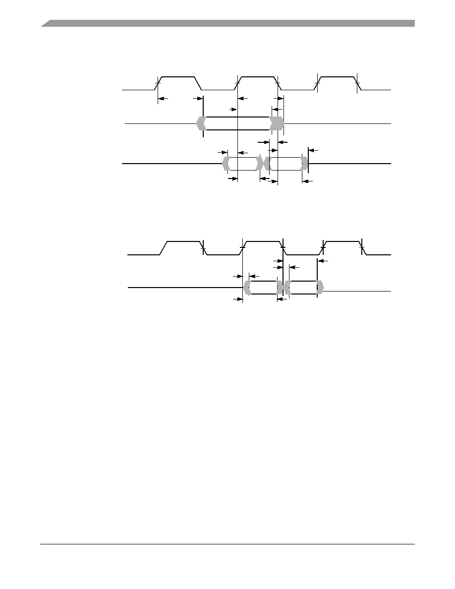
MPC7455 RISC Microprocessor Hardware Specifications, Rev. 4.1
26
Freescale Semiconductor
Electrical and Thermal Characteristics
Figure 10
shows the L3 bus timing diagrams for the MPC7455 interfaced to MSUG2 SRAMs.
Figure 10. L3 Bus Timing Diagrams for L3 Cache DDR SRAMs
5.2.4.2 L3 Bus AC Specifications for PB2 and Late Write SRAMs
When using PB2 or late write SRAMs at the L3 interface, the parts should be connected as shown in
Figure 11
.
These SRAMs are synchronous to the MPC7455; one L3_CLKn signal is output to each SRAM to latch address,
control, and write data. Read data is launched by the SRAM synchronous to the delayed L3_CLKn signal it received.
The MPC7455 needs a copy of that delayed clock which launched the SRAM read data to know when the returning
data will be valid. Therefore, L3_ECHO_CLK1 and L3_ECHO_CLK3 must be routed halfway to the SRAMs and
then returned to the MPC7455 inputs L3_ECHO_CLK0 and L3_ECHO_CLK2, respectively. Thus,
L3_ECHO_CLK0 and L3_ECHO_CLK2 are phase-aligned with the input clock received at the SRAMs. The
MPC7455 will latch the incoming data on the rising edge of L3_ECHO_CLK0 and L3_ECHO_CLK2.
L3_ECHO_CLK[0,1,2,3]
L3 Data and Data
VM
VM = Midpoint Voltage (GV
DD
/2)
Parity Inputs
L3_CLK[0,1]
ADDR, L3CNTL
VM
t
L3CHOV
t
L3CHOX
VM
L3DATA WRITE
t
L3CHOZ
VM
VM
VM
VM
t
L3CHDV
t
L3CHDX
VM
VM
VM
Outputs
Inputs
t
L3CLDV
t
L3CLDX
t
L3CLDZ
t
L3DVEH
t
L3DXEL
t
L3DVEL
t
L3DXEH
Note: t
L3DVEH
and t
L3DVEL
as drawn here will be negative numbers, that is, input setup time will be
time after the clock edge.
Note: t
L3CHDV
and t
L3CLDV
as drawn here will be negative numbers, that is, output valid time will be
time before the clock edge.
VM = Midpoint Voltage (GV
DD
/2)
MPC7455 RISC Microprocessor Hardware Specifications, Rev. 4.1
Freescale Semiconductor
27
Electrical and Thermal Characteristics
Table 13
provides the L3 bus interface AC timing specifications for the configuration shown in
Figure 11
, assuming
the timing relationships of
Figure 12
and the loading of
Figure 8
.
Table 13. L3 Bus Interface AC Timing Specifications for PB2 and Late Write SRAMs
At recommended operating conditions. See
Table 4
.
Parameter
Symbol
All Speed Grades
6
Unit Notes
L3OH0 = 0, L3OH1 = 0 L3OH0 = 0, L3OH1 =1 L3OH0 = 1, L3OH1 = 0 L3OH0 = 1, L3OH1 = 1
Min
Max
Min
Max
Min
Max
Min
Max
L3_CLK rise
and fall time
t
L3CR
,
t
L3CF
--
1.0
--
1.0
--
1.0
--
1.0
ns
1, 5
Setup times:
Data and
parity
t
L3DVEH
1.5
--
1.5
--
1.5
--
1.5
--
ns
2, 5
Input hold
times: Data
and parity
t
L3DXEH
--
0.5
--
0.5
--
0.5
--
0.5
ns
2, 5
Valid times:
Data and
parity
t
L3CHDV
--
t
L3_CLK
/4
+ 1.00
--
t
L3_CLK
/4
+ 0.80
--
t
L3_CLK
/4
+ 0.60
--
t
L3_CLK
/4
+ 0.40
ns
3, 4, 5
Valid times: All
other outputs
t
L3CHOV
--
t
L3_CLK
/4
+ 1.00
--
t
L3_CLK
/4
+ 0.80
--
t
L3_CLK
/4
+ 0.60
--
t
L3_CLK
/4
+ 0.40
ns
4
Output hold
times: Data
and parity
t
L3CHDX
t
L3_CLK
/4
� 0.40
--
t
L3_CLK
/4
� 0.60
--
t
L3_CLK
/4
� 0.80
--
t
L3_CLK
/4
� 1.00
--
ns
3, 4, 5
Output hold
times: All other
outputs
t
L3CHOX
t
L3_CLK
/4
� 0.40
--
t
L3_CLK
/4
� 0.60
--
t
L3_CLK
/4
� 0.80
--
t
L3_CLK
/4
� 1.00
--
ns
4, 5
L3_CLK to
high
impedance:
Data and
parity
t
L3CHDZ
--
2.0
--
2.0
--
2.0
--
2.0
ns
5
MPC7455 RISC Microprocessor Hardware Specifications, Rev. 4.1
28
Freescale Semiconductor
Electrical and Thermal Characteristics
L3_CLK to
high
impedance: All
other outputs
t
L3CHOZ
--
2.0
--
2.0
--
2.0
--
2.0
ns
5
Notes:
1. Rise and fall times for the L3_CLK output are measured from 20% to 80% of GV
DD
.
2. All input specifications are measured from the midpoint of the signal in question to the midpoint voltage of the rising edge of
the input L3_ECHO_CLK
n (see
Figure 10
). Input timings are measured at the pins.
3. All output specifications are measured from the midpoint voltage of the rising edge of L3_CLK
n to the midpoint of the signal
in question. The output timings are measured at the pins. All output timings assume a purely resistive 50-
load (see
Figure 10
).
4. t
L3_CLK
/4 is one-fourth the period of L3_CLK
n. This parameter indicates that the specified output signal is actually launched
by an internal clock delayed in phase by 90�. Therefore, there is a frequency component to the output valid and output hold
times such that the specified output signal will be valid for approximately one L3_CLK period starting three-fourths of a clock
prior to the edge on which the SRAM will sample it and ending one-fourth of a clock period after the edge it will be sampled.
5. Timing behavior and characterization are currently being evaluated.
6. These configuration bits allow the AC timing of the L3 interface to be altered via software. L3OH0 = L2CR[12],
L30H1 = L3CR[12]. Revisions of the MPC7455 not described by this document may implement these bits differently. See
Section 11.1, "Part Numbers Fully Addressed by This Document,"
and
Section 11.2, "Part Numbers Not Fully Addressed by
This Document,"
for more information on which devices are addressed by this document.
Table 13. L3 Bus Interface AC Timing Specifications for PB2 and Late Write SRAMs (continued)
At recommended operating conditions. See
Table 4
.
Parameter
Symbol
All Speed Grades
6
Unit Notes
L3OH0 = 0, L3OH1 = 0 L3OH0 = 0, L3OH1 =1 L3OH0 = 1, L3OH1 = 0 L3OH0 = 1, L3OH1 = 1
Min
Max
Min
Max
Min
Max
Min
Max
MPC7455 RISC Microprocessor Hardware Specifications, Rev. 4.1
Freescale Semiconductor
29
Electrical and Thermal Characteristics
Figure 11
shows the typical connection diagram for the MPC7455 interfaced to PB2 SRAMs, such as the Freescale
MCM63R737, or late write SRAMs, such as the Freescale MCM63R836A.
Figure 11. Typical Synchronous 1-MByte L3 Cache Late Write or PB2 Interface
L3_ADDR[16:0]
L3_CNTL[0]
SA[16:0]
K
K
SS
SW
ZZ
G
SRAM 0
DQ[0:17]
DQ[18:36
]
L3_CNTL[1]
GV
DD
/2
1
GND
GND
SRAM 1
GV
DD
/2
1
GND
GND
{L3_DATA[0:15],
{L3_DATA[16:31],
{L3_DATA[32:47],
L3_CLK[0]
L3_CLK[1]
L3_ECHO_CLK[0]
L3_ECHO_CLK[1]
L3_ECHO_CLK[2]
{L3_DATA[48:63],
L3_DP[0:1]}
L3_DP[2:3]}
L3_DP[4:5]}
L3_DP[6:7]}
Denotes
Receive (SRAM
to MPC7455)
Aligned Signals
MPC7455
Denotes
Transmit
(MPC7455 to
SRAM)
Aligned Signals
L3_ECHO_CLK[3]
SA[16:0]
K
K
SS
SW
ZZ
G
DQ[0:17]
DQ[18:36
]
Note:
1. Or as recommended by SRAM manufacturer for single-ended clocking.
MPC7455 RISC Microprocessor Hardware Specifications, Rev. 4.1
30
Freescale Semiconductor
Electrical and Thermal Characteristics
Figure 12
shows the L3 bus timing diagrams for the MPC7455 interfaced to PB2 or late write SRAMs.
Figure 12. L3 Bus Timing Diagrams for Late Write or PB2 SRAMs
5.2.5 IEEE 1149.1 AC Timing Specifications
Table 14
provides the IEEE 1149.1 (JTAG) AC timing specifications as defined in
Figure 14
through
Figure 17
.
Table 14. JTAG AC Timing Specifications (Independent of SYSCLK)
1
At recommended operating conditions. See
Table 4
.
Parameter
Symbol
Min
Max
Unit
Notes
TCK frequency of operation
f
TCLK
0
33.3
MHz
TCK cycle time
t
TCLK
30
--
ns
TCK clock pulse width measured at 1.4 V
t
JHJL
15
--
ns
TCK rise and fall times
t
JR
and t
JF
0
2
ns
TRST assert time
t
TRST
25
--
ns
2
Input setup times:
Boundary-scan data
TMS, TDI
t
DVJH
t
IVJH
4
0
--
--
ns
3
Input hold times:
Boundary-scan data
TMS, TDI
t
DXJH
t
IXJH
20
25
--
--
ns
3
L3_ECHO_CLK[0,2]
L3 Data and Data
VM
VM = Midpoint Voltage (GV
DD
/2)
t
L3DVEH
t
L3DXEH
Parity Inputs
L3_CLK[0,1]
ADDR, L3_CNTL
VM
t
L3CHOV
t
L3CHOX
VM
L3DATA WRITE
t
L3CHDZ
Outputs
Inputs
L3_ECHO_CLK[1,3]
t
L3CHDV
t
L3CHDX
t
L3CHOZ

MPC7455 RISC Microprocessor Hardware Specifications, Rev. 4.1
Freescale Semiconductor
31
Electrical and Thermal Characteristics
Figure 13
provides the AC test load for TDO and the boundary-scan outputs of the MPC7455.
Figure 13. Alternate AC Test Load for the JTAG Interface
Figure 14
provides the JTAG clock input timing diagram.
Figure 14. JTAG Clock Input Timing Diagram
Figure 15
provides the TRST timing diagram.
Figure 15. TRST Timing Diagram
Valid times:
Boundary-scan data
TDO
t
JLDV
t
JLOV
4
4
20
25
ns
4
Output hold times:
Boundary-scan data
TDO
t
JLDX
t
JLOX
TBD
TBD
TBD
TBD
ns
4
TCK to output high impedance:
Boundary-scan data
TDO
t
JLDZ
t
JLOZ
3
3
19
9
ns
4, 5
Notes:
1. All outputs are measured from the midpoint voltage of the falling/rising edge of TCLK to the midpoint of the signal
in question. The output timings are measured at the pins. All output timings assume a purely resistive 50-
load
(see
Figure 13
). Time-of-flight delays must be added for trace lengths, vias, and connectors in the system.
2. TRST is an asynchronous level sensitive signal. The setup time is for test purposes only.
3. Non-JTAG signal input timing with respect to TCK.
4. Non-JTAG signal output timing with respect to TCK.
5. Guaranteed by design and characterization.
Table 14. JTAG AC Timing Specifications (Independent of SYSCLK)
1
(continued)
At recommended operating conditions. See
Table 4
.
Parameter
Symbol
Min
Max
Unit
Notes
Output
Z
0
= 50
OV
DD
/2
R
L
= 50
VM
VM
VM
VM = Midpoint Voltage (OV
DD
/2)
t
TCLK
t
JR
t
JF
t
JHJL
TCLK
TRST
t
TRST
VM = Midpoint Voltage (OV
DD
/2)
VM
VM
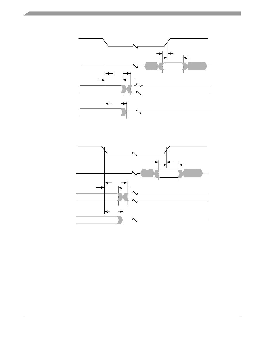
MPC7455 RISC Microprocessor Hardware Specifications, Rev. 4.1
32
Freescale Semiconductor
Electrical and Thermal Characteristics
Figure 16
provides the boundary-scan timing diagram.
Figure 16. Boundary-Scan Timing Diagram
Figure 17
provides the test access port timing diagram.
Figure 17. Test Access Port Timing Diagram
VM
TCK
Boundary
Boundary
Boundary
Data Outputs
Data Inputs
Data Outputs
VM = Midpoint Voltage (OV
DD
/2)
t
DXJH
t
DVJH
t
JLDV
t
JLDZ
Input
Data Valid
Output Data Valid
Output Data Valid
t
JLDX
VM
VM
TCK
TDI, TMS
TDO
Output Data Valid
VM
= Midpoint Voltage (OV
DD
/2)
t
IXJH
t
IVJH
t
JLOV
t
JLOZ
Input
Data Valid
TDO
Output Data Valid
t
JLOX
VM
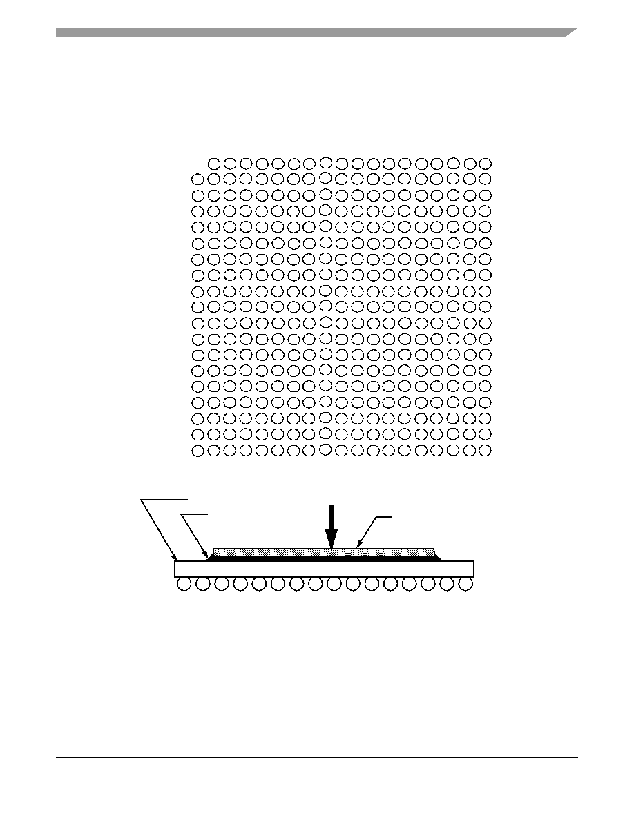
MPC7455 RISC Microprocessor Hardware Specifications, Rev. 4.1
Freescale Semiconductor
33
Pin Assignments
6
Pin Assignments
Figure 18
(in Part A) shows the pinout of the MPC7445, 360 CBGA package as viewed from the top surface. Part B
shows the side profile of the CBGA package to indicate the direction of the top surface view.
Figure 18. Pinout of the MPC7445, 360 CBGA Package as Viewed from the Top Surface
A
B
C
D
E
F
G
H
J
K
L
M
N
P
R
T
1
2
3
4
5
6
7
8
9
10 11 12 13 14 15 16
Not to Scale
17 18 19
U
V
W
Part A
View
Part B
Die
Substrate Assembly
Encapsulant
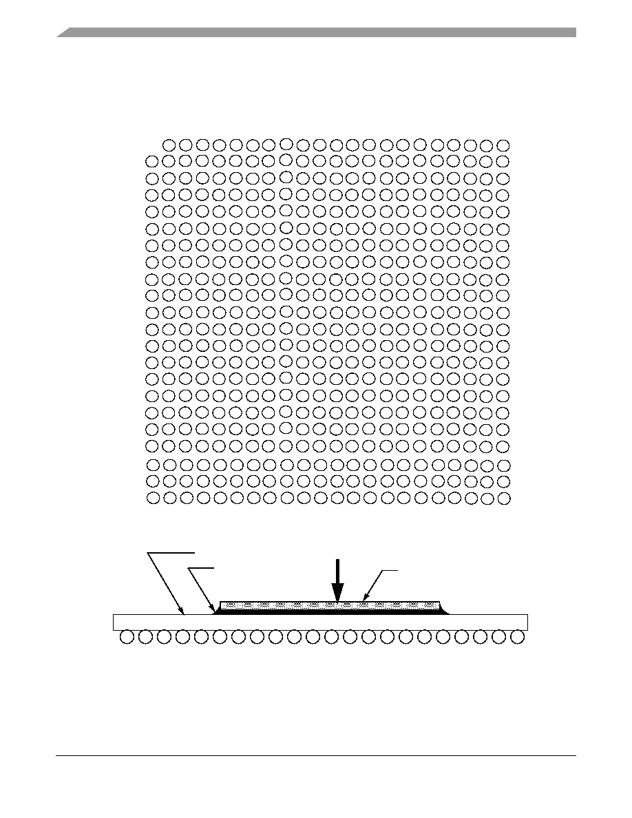
MPC7455 RISC Microprocessor Hardware Specifications, Rev. 4.1
34
Freescale Semiconductor
Pin Assignments
Figure 19
(in Part A) shows the pinout of the MPC7455, 483 CBGA package as viewed from the top surface. Part B
shows the side profile of the CBGA package to indicate the direction of the top surface view.
Figure 19. Pinout of the MPC7455, 483 CBGA Package as Viewed from the Top Surface
A
B
C
D
E
F
G
H
J
K
L
M
N
P
R
T
1
2
3
4
5
6
7
8
9
10 11 12 13 14 15 16
Not to Scale
17 18 19
U
V
W
20 21 22
Y
AA
AB
Part A
View
Part B
Die
Substrate Assembly
Encapsulant

MPC7455 RISC Microprocessor Hardware Specifications, Rev. 4.1
Freescale Semiconductor
35
Pinout Listings
7
Pinout Listings
Table 15
provides the pinout listing for the MPC7445, 360 CBGA package.
Table 16
provides the pinout listing for
the MPC7455, 483 CBGA package.
NOTE
This pinout is not compatible with the MPC750, MPC7400, or MPC7410, 360
BGA package.
Table 15. Pinout Listing for the MPC7445, 360 CBGA Package
Signal Name
Pin Number
Active
I/O
I/F Select
1
Notes
A[0:35]
E11, H1, C11, G3, F10, L2, D11, D1, C10,
G2, D12, L3, G4, T2, F4, V1, J4, R2, K5,
W2, J2, K4, N4, J3, M5, P5, N3, T1, V2,
U1, N5, W1, B12, C4, G10, B11
High
I/O
BVSEL
11
AACK
R1
Low
Input
BVSEL
AP[0:4]
C1, E3, H6, F5, G7
High
I/O
BVSEL
ARTRY
N2
Low
I/O
BVSEL
8
AV
DD
A8
--
Input
N/A
BG
M1
Low
Input
BVSEL
BMODE0
G9
Low
Input
BVSEL
5
BMODE1
F8
Low
Input
BVSEL
6
BR
D2
Low
Output
BVSEL
BVSEL
B7
High
Input
BVSEL
1, 7
CI
J1
Low
Output
BVSEL
8
CKSTP_IN
A3
Low
Input
BVSEL
CKSTP_OUT
B1
Low
Output
BVSEL
CLK_OUT
H2
High
Output
BVSEL
D[0:63]
R15, W15, T14, V16, W16, T15, U15,
P14, V13, W13, T13, P13, U14, W14,
R12, T12, W12, V12, N11, N10, R11, U11,
W11, T11, R10, N9, P10, U10, R9, W10,
U9, V9, W5, U6, T5, U5, W7, R6, P7, V6,
P17, R19, V18, R18, V19, T19, U19, W19,
U18, W17, W18, T16, T18, T17, W3, V17,
U4, U8, U7, R7, P6, R8, W8, T8
High
I/O
BVSEL
DBG
M2
Low
Input
BVSEL
DP[0:7]
T3, W4, T4, W9, M6, V3, N8, W6
High
I/O
BVSEL
DRDY
R3
Low
Output
BVSEL
4
DTI[0:3]
G1, K1, P1, N1
High
Input
BVSEL
13
EXT_QUAL
A11
High
Input
BVSEL
9

MPC7455 RISC Microprocessor Hardware Specifications, Rev. 4.1
36
Freescale Semiconductor
Pinout Listings
GBL
E2
Low
I/O
BVSEL
GND
B5, C3, D6, D13, E17, F3, G17, H4, H7,
H9, H11, H13, J6, J8, J10, J12, K7, K3,
K9, K11, K13, L6, L8, L10, L12, M4, M7,
M9, M11, M13, N7, P3, P9, P12, R5, R14,
R17, T7, T10, U3, U13, U17, V5, V8, V11,
V15
--
--
N/A
HIT
B2
Low
Output
BVSEL
4
HRESET
D8
Low
Input
BVSEL
INT
D4
Low
Input
BVSEL
L1_TSTCLK G8
High
Input
BVSEL
9
L2_TSTCLK
B3
High
Input
BVSEL
12
No Connect
A6, A13, A14, A15, A16, A17, A18, A19,
B13, B14, B15, B16, B17, B18, B19, C13,
C14, C15, C16, C17, C18, C19, D14, D15,
D16, D17, D18, D19, E12, E13, E14, E15,
E16, E19, F12, F13, F14, F15, F16, F17,
F18, F19, G11, G12, G13, G14, G15,
G16, G19, H14, H15, H16, H17, H18,
H19, J14, J15, J16, J17, J18, J19, K15,
K16, K17, K18, K19, L14, L15, L16, L17,
L18, L19, M14, M15, M16, M17, M18,
M19, N12, N13, N14, N15, N16, N17,
N18, N19, P15, P16, P18, P19
--
--
--
3
LSSD_MODE
E8
Low
Input
BVSEL
2, 7
MCP
C9
Low
Input
BVSEL
OV
DD
B4, C2, C12, D5, E18, F2, G18, H3, J5,
K2, L5, M3, N6, P2, P8, P11, R4, R13,
R16, T6, T9, U2, U12, U16, V4, V7, V10,
V14
--
--
N/A
PLL_CFG[0:4]
B8, C8, C7, D7, A7
High
Input
BVSEL
PMON_IN
D9
Low
Input
BVSEL
10
PMON_OUT
A9
Low
Output
BVSEL
QACK
G5
Low
Input
BVSEL
QREQ
P4
Low
Output
BVSEL
SHD[0:1]
E4, H5
Low
I/O
BVSEL
8
SMI
F9
Low
Input
BVSEL
SRESET
A2
Low
Input
BVSEL
SYSCLK
A10
--
Input
BVSEL
TA
K6
Low
Input
BVSEL
Table 15. Pinout Listing for the MPC7445, 360 CBGA Package (continued)
Signal Name
Pin Number
Active
I/O
I/F Select
1
Notes

MPC7455 RISC Microprocessor Hardware Specifications, Rev. 4.1
Freescale Semiconductor
37
Pinout Listings
TBEN
E1
High
Input
BVSEL
TBST
F11
Low
Output
BVSEL
TCK
C6
High
Input
BVSEL
TDI
B9
High
Input
BVSEL
7
TDO
A4
High
Output
BVSEL
TEA
L1
Low
Input
BVSEL
TEST[0:3]
A12, B6, B10, E10
--
Input
BVSEL
2
TEST[4]
D10
--
Input
BVSEL
9
TMS
F1
High
Input
BVSEL
7
TRST
A5
Low
Input
BVSEL
7, 14
TS
L4
Low
I/O
BVSEL
8
TSIZ[0:2]
G6, F7, E7
High
Output
BVSEL
TT[0:4]
E5, E6, F6, E9, C5
High
I/O
BVSEL
WT
D3
Low
Output
BVSEL
8
V
DD
H8, H10, H12, J7, J9, J11, J13, K8, K10,
K12, K14, L7, L9, L11, L13, M8, M10, M12
--
--
N/A
Notes:
1. OV
DD
supplies power to the processor bus, JTAG, and all control signals; and V
DD
supplies power to the processor
core and the PLL (after filtering to become AV
DD
). To program the I/O voltage, connect BVSEL to either GND
(selects 1.8 V) or to HRESET (selects 2.5 V). If used, the pulldown resistor should be less than 250
. For actual
recommended value of V
in
or supply voltages see
Table 4
.
2. These input signals are for factory use only and must be pulled up to OV
DD
for normal machine operation.
3. These signals are for factory use only and must be left unconnected for normal machine operation.
4. Ignored in 60x bus mode.
5. This signal selects between MPX bus mode (asserted) and 60x bus mode (negated) and will be sampled at
HRESET going high.
6. This signal must be negated during reset, by pull-up to OV
DD
or negation by �HRESET (inverse of HRESET), to
ensure proper operation.
7. Internal pull-up on die.
8. These pins require weak pull-up resistors (for example, 4.7 k
) to maintain the control signals in the negated state
after they have been actively negated and released by the MPC7445 and other bus masters.
9. These input signals are for factory use only and must be pulled down to GND for normal machine operation.
10.This pin can externally cause a performance monitor event. Counting of the event is enabled via software.
11.Unused address pins must be pulled down to GND.
12.This test signal is recommended to be tied to HRESET; however, other configurations will not adversely affect
performance.
13.These signals must be pulled down to GND if unused, or if the MPC7445 is in 60x bus mode.
14.This signal must be asserted during reset, by pull-down to GND or assertion by HRESET, to ensure proper
operation.
Table 15. Pinout Listing for the MPC7445, 360 CBGA Package (continued)
Signal Name
Pin Number
Active
I/O
I/F Select
1
Notes
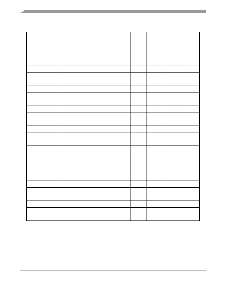
MPC7455 RISC Microprocessor Hardware Specifications, Rev. 4.1
38
Freescale Semiconductor
Pinout Listings
Table 16. Pinout Listing for the MPC7455, 483 CBGA Package
Signal Name
Pin Number
Active
I/O
I/F Select
1
Notes
A[0:35]
E10, N4, E8, N5, C8, R2, A7, M2, A6, M1,
A10, U2, N2, P8, M8, W4, N6, U6, R5, Y4, P1,
P4, R6, M7, N7, AA3, U4, W2, W1, W3, V4,
AA1, D10, J4, G10, D9
High
I/O
BVSEL
11
AACK
U1
Low
Input
BVSEL
AP[0:4]
L5, L6, J1, H2, G5
High
I/O
BVSEL
ARTRY
T2
Low
I/O
BVSEL
8
AV
DD
B2
--
Input
N/A
BG
R3
Low
Input
BVSEL
BMODE0
C6
Low
Input
BVSEL
5
BMODE1
C4
Low
Input
BVSEL
6
BR
K1
Low
Output
BVSEL
BVSEL
G6
High
Input
N/A
3, 7
CI
R1
Low
Output
BVSEL
8
CKSTP_IN
F3
Low
Input
BVSEL
CKSTP_OUT
K6
Low
Output
BVSEL
CLK_OUT
N1
High
Output
BVSEL
D[0:63]
AB15, T14, R14, AB13, V14, U14, AB14,
W16, AA11, Y11, U12, W13, Y14, U13, T12,
W12, AB12, R12, AA13, AB11, Y12, V11, T11,
R11, W10, T10, W11, V10, R10, U10, AA10,
U9, V7, T8, AB4, Y6, AB7, AA6, Y8, AA7, W8,
AB10, AA16, AB16, AB17, Y18, AB18, Y16,
AA18, W14, R13, W15, AA14, V16, W6,
AA12, V6, AB9, AB6, R7, R9, AA9, AB8, W9
High
I/O
BVSEL
DBG
V1
Low
Input
BVSEL
DP[0:7]
AA2, AB3, AB2, AA8, R8, W5, U8, AB5
High
I/O
BVSEL
DRDY
T6
Low
Output
BVSEL
4
DTI[0:3]
P2, T5, U3, P6
High
Input
BVSEL
13
EXT_QUAL
B9
High
Input
BVSEL
9
GBL
M4
Low
I/O
BVSEL
MPC7455 RISC Microprocessor Hardware Specifications, Rev. 4.1
Freescale Semiconductor
39
Pinout Listings
GND
A22, B1, B5, B12, B14, B16, B18, B20, C3,
C9, C21, D7, D13, D15, D17, D19, E2, E5,
E21, F10, F12, F14, F16, F19, G4, G7, G17,
G21, H13, H15, H19, H5, J3, J10, J12, J14,
J17, J21, K5, K9, K11, K13, K15, K19, L10,
L12, L14, L17, L21, M3, M6, M9, M11, M13,
M19, N10, N12, N14, N17, N21, P3, P9, P11,
P13, P15, P19, R17, R21, T13, T15, T19, T4,
T7, T9, U17, U21, V2, V5, V8, V12, V15, V19,
W7, W17, W21, Y3, Y9, Y13, Y15, Y20, AA5,
AA17, AB1, AB22
--
--
N/A
GV
DD
B13, B15, B17, B19, B21, D12, D14, D16,
D18, D21, E19, F13, F15, F17, F21, G19,
H12, H14, H17, H21, J19, K17, K21, L19,
M17, M21, N19, P17, P21, R15, R19, T17,
T21, U19, V17, V21, W19, Y21
--
--
N/A
15
HIT
K2
Low
Output
BVSEL
4
HRESET
A3
Low
Input
BVSEL
INT
J6
Low
Input
BVSEL
L1_TSTCLK H4
High
Input
BVSEL
9
L2_TSTCLK
J2
High
Input
BVSEL
12
L3VSEL
A4
High
Input
N/A
3, 7
L3ADDR[17:0]
F20, J16, E22, H18, G20, F22, G22, H20,
K16, J18, H22, J20, J22, K18, K20, L16, K22,
L18
High
Output
L3VSEL
L3_CLK[0:1]
V22, C17
High
Output
L3VSEL
L3_CNTL[0:1]
L20, L22
Low
Output
L3VSEL
L3DATA[0:63]
AA19, AB20, U16, W18, AA20, AB21, AA21,
T16, W20, U18, Y22, R16, V20, W22, T18,
U20, N18, N20, N16, N22, M16, M18, M20,
M22, R18, T20, U22, T22, R20, P18, R22,
M15, G18, D22, E20, H16, C22, F18, D20,
B22, G16, A21, G15, E17, A20, C19, C18,
A19, A18, G14, E15, C16, A17, A16, C15,
G13, C14, A14, E13, C13, G12, A13, E12,
C12
High
I/O
L3VSEL
L3DP[0:7]
AB19, AA22, P22, P16, C20, E16, A15, A12
High
I/O
L3VSEL
L3_ECHO_CLK[0,2]
V18, E18
High
Input
L3VSEL
L3_ECHO_CLK[1,3]
P20, E14
HIgh
I/O
L3VSEL
LSSD_MODE
F6
Low
Input
BVSEL
2, 7
MCP
B8
Low
Input
BVSEL
Table 16. Pinout Listing for the MPC7455, 483 CBGA Package (continued)
Signal Name
Pin Number
Active
I/O
I/F Select
1
Notes
MPC7455 RISC Microprocessor Hardware Specifications, Rev. 4.1
40
Freescale Semiconductor
Pinout Listings
No Connect
A8, A11, B6, B11, C11, D11, D3, D5, E11, E7,
F2, F11, G11, G2, H11, H9, J8
--
--
N/A
16
OV
DD
B3, C5, C7, C10, D2, E3, E9, F5, G3, G9, H7,
J5, K3, L7, M5, N3, P7, R4, T3, U5, U7, U11,
U15, V3, V9, V13, Y2, Y5, Y7, Y10, Y17, Y19,
AA4, AA15
--
--
N/A
PLL_CFG[0:4]
A2, F7, C2, D4, H8
High
Input
BVSEL
PMON_IN
E6
Low
Input
BVSEL
10
PMON_OUT
B4
Low
Output
BVSEL
QACK
K7
Low
Input
BVSEL
QREQ
Y1
Low
Output
BVSEL
SHD[0:1]
L4, L8
Low
I/O
BVSEL
8
SMI
G8
Low
Input
BVSEL
SRESET
G1
Low
Input
BVSEL
SYSCLK
D6
--
Input
BVSEL
TA
N8
Low
Input
BVSEL
TBEN
L3
High
Input
BVSEL
TBST
B7
Low
Output
BVSEL
TCK
J7
High
Input
BVSEL
TDI
E4
High
Input
BVSEL
7
TDO
H1
High
Output
BVSEL
TEA
T1
Low
Input
BVSEL
TEST[0:5]
B10, H6, H10, D8, F9, F8
--
Input
BVSEL
2
TEST[6]
A9
--
Input
BVSEL
9
TMS
K4
High
Input
BVSEL
7
TRST
C1
Low
Input
BVSEL
7, 14
TS
P5
Low
I/O
BVSEL
8
TSIZ[0:2]
L1,H3,D1
High
Output
BVSEL
TT[0:4]
F1, F4, K8, A5, E1
High
I/O
BVSEL
WT
L2
Low
Output
BVSEL
8
Table 16. Pinout Listing for the MPC7455, 483 CBGA Package (continued)
Signal Name
Pin Number
Active
I/O
I/F Select
1
Notes

MPC7455 RISC Microprocessor Hardware Specifications, Rev. 4.1
Freescale Semiconductor
41
Package Description
8
Package Description
The following sections provide the package parameters and mechanical dimensions for the CBGA package.
8.1 Package Parameters for the MPC7445, 360 CBGA
The package parameters are as provided in the following list. The package type is 25
� 25 mm, 360-lead ceramic
ball grid array (CBGA).
Package outline
25
� 25 mm
Interconnects
360 (19
� 19 ball array � 1)
Pitch
1.27 mm (50 mil)
Minimum module height
2.72 mm
Maximum module height
3.24 mm
Ball diameter
0.89 mm (35 mil)
V
DD
J9, J11, J13, J15, K10, K12, K14, L9, L11,
L13, L15, M10, M12, M14, N9, N11, N13, N15,
P10, P12, P14
--
--
N/A
Notes:
1. OV
DD
supplies power to the processor bus, JTAG, and all control signals except the L3 cache controls (L3CTL[0:1]);
GV
DD
supplies power to the L3 cache interface (L3ADDR[0:17], L3DATA[0:63], L3DP[0:7], L3_ECHO_CLK[0:3],
and L3_CLK[0:1]) and the L3 control signals L3_CNTL[0:1]; and V
DD
supplies power to the processor core and the
PLL (after filtering to become AV
DD
). For actual recommended value of V
in
or supply voltages, see
Table 4
.
2. These input signals are for factory use only and must be pulled up to OV
DD
for normal machine operation.
3. To program the processor interface I/O voltage, connect BVSEL to either GND (selects 1.8 V) or to HRESET (selects
2.5 V). To program the L3 interface, connect L3VSEL to either GND (selects 1.8 V) or to HRESET (selects 2.5 V)
or to HRESET (selects 1.5 V). If used, pulldown resistors should be less than 250
.
4. Ignored in 60x bus mode.
5. This signal selects between MPX bus mode (asserted) and 60x bus mode (negated) and will be sampled at
HRESET going high.
6. This signal must be negated during reset, by pull-up to OV
DD
or negation by �HRESET (inverse of HRESET), to
ensure proper operation.
7. Internal pull-up on die.
8. These pins require weak pull-up resistors (for example, 4.7 k
) to maintain the control signals in the negated state
after they have been actively negated and released by the MPC7455 and other bus masters.
9. These input signals for factory use only and must be pulled down to GND for normal machine operation.
10.This pin can externally cause a performance monitor event. Counting of the event is enabled via software.
11.Unused address pins must be pulled down to GND.
12.This test signal is recommended to be tied to HRESET; however, other configurations will not adversely affect
performance.
13.These signals must be pulled down to GND if unused or if the MPC7455 is in 60x bus mode.
14.This signal must be asserted during reset, by pull-down to GND or assertion by HRESET, to ensure proper
operation.
15.Power must be supplied to GV
DD
, even when the L3 interface is disabled or unused.
16.These signals are for factory use only and must be left unconnected for normal machine operation.
Table 16. Pinout Listing for the MPC7455, 483 CBGA Package (continued)
Signal Name
Pin Number
Active
I/O
I/F Select
1
Notes
MPC7455 RISC Microprocessor Hardware Specifications, Rev. 4.1
42
Freescale Semiconductor
Package Description
8.2 Mechanical Dimensions for the MPC7445, 360 CBGA
Figure 20
provides the mechanical dimensions and
bottom surface nomenclature for the MPC7445, 360 CBGA
package.
Figure 20. Mechanical Dimensions and Bottom Surface Nomenclature for the MPC7445,
360 CBGA Package
NOTES:
1. DIMENSIONING AND TOLERANCING
PER ASME Y14.5M, 1994.
2. DIMENSIONS IN MILLIMETERS.
3. TOP SIDE A1 CORNER INDEX IS A
METALIZED FEATURE WITH VARIOUS
SHAPES. BOTTOM SIDE A1 CORNER IS
DESIGNATED WITH A BALL MISSING
FROM THE ARRAY.
0.2
C
A
360X
D
2X
A1 CORNER
E
e
0.2
2X
C
B
1 2 3 4 5 6 7 8 9 10 11 1213141516
A
B
C
D
E
F
G
H
J
K
L
M
N
P
R
T
B
0.3
A
0.15
b
A
0.15 A
17 18 19
U
W
V
Millimeters
DIM
MIN
MAX
A
2.72
3.20
A1
0.80
1.00
A2
1.10
1.30
A3
--
0.6
b
0.82
0.93
D
25.00 BSC
D1
--
6.15
D2
12.15
12.45
e
1.27 BSC
E
25.00 BSC
E1
--
11.1
E2
7.45
--
E3
8.75
9.20
Capacitor Region
1
D1
E2
E1
A
A1
A2
A3
E3
D2
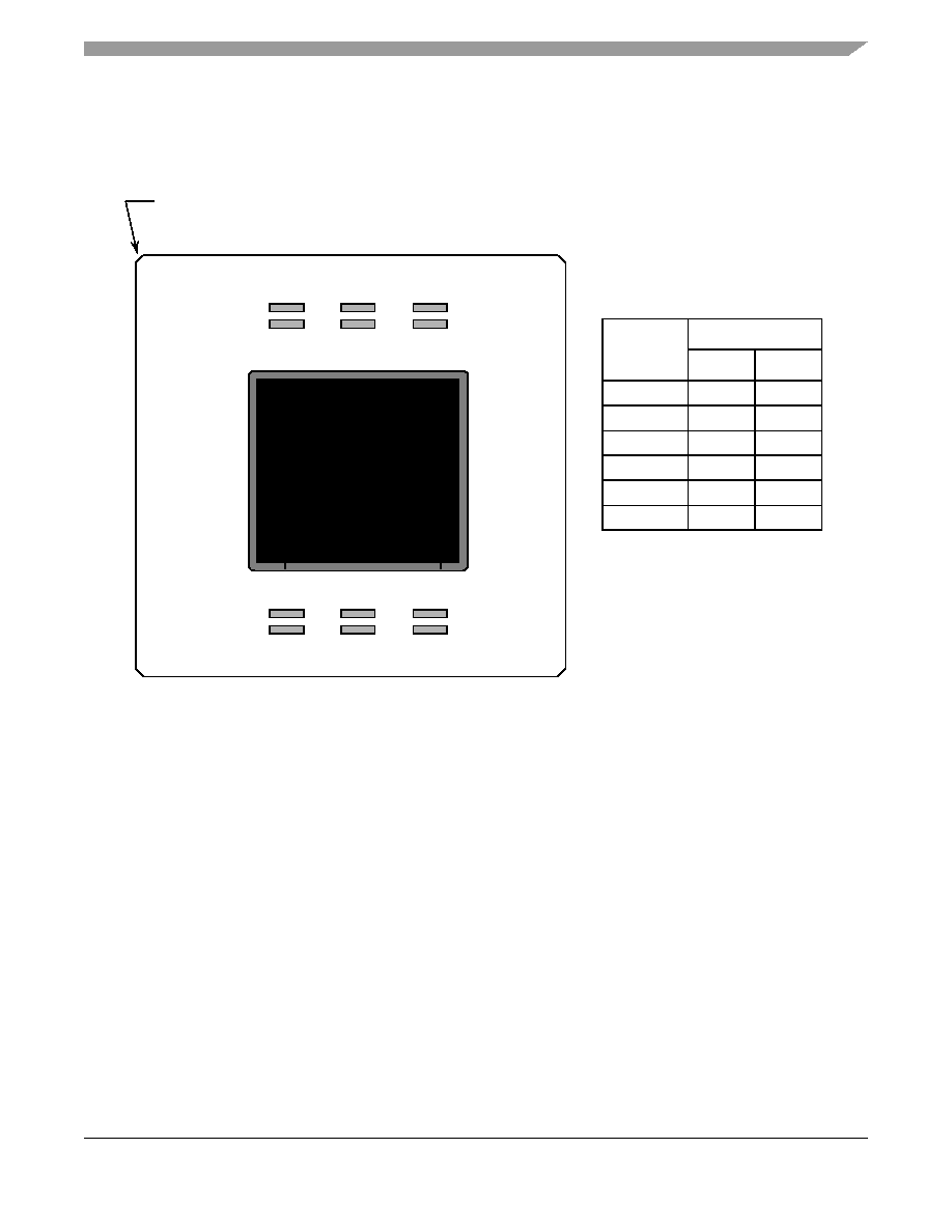
MPC7455 RISC Microprocessor Hardware Specifications, Rev. 4.1
Freescale Semiconductor
43
Package Description
8.3 Substrate Capacitors for the MPC7445, 360 CBGA
Figure 21
shows the connectivity of the substrate capacitor pads for the MPC7445, 360 CBGA. All capacitors are
100 nF.
Figure 21. Substrate Bypass Capacitors for the MPC7445, 360 CBGA
8.4 Package Parameters for the MPC7455, 483 CBGA
The package parameters are as provided in the following list. The package type is 29
� 29 mm, 483-lead ceramic
ball grid array (CBGA).
Package outline
29
� 29 mm
Interconnects
483 (22
� 22 ball array � 1)
Pitch
1.27 mm (50 mil)
Minimum module height
--
Maximum module height
3.22 mm
Ball diameter
0.89 mm (35 mil)
Capacitor
Pad Number
-1
-2
C1
OV
DD
GND
C2
V
DD
GND
C3
OV
DD
GND
C4
V
DD
GND
C5
OV
DD
GND
C6
V
DD
GND
1
C3-1
C3-2
C2-2
C1-2
C1-1
C2-1
A1 Corner
C4-1
C4-2
C5-2
C6-2
C6-1
C5-1
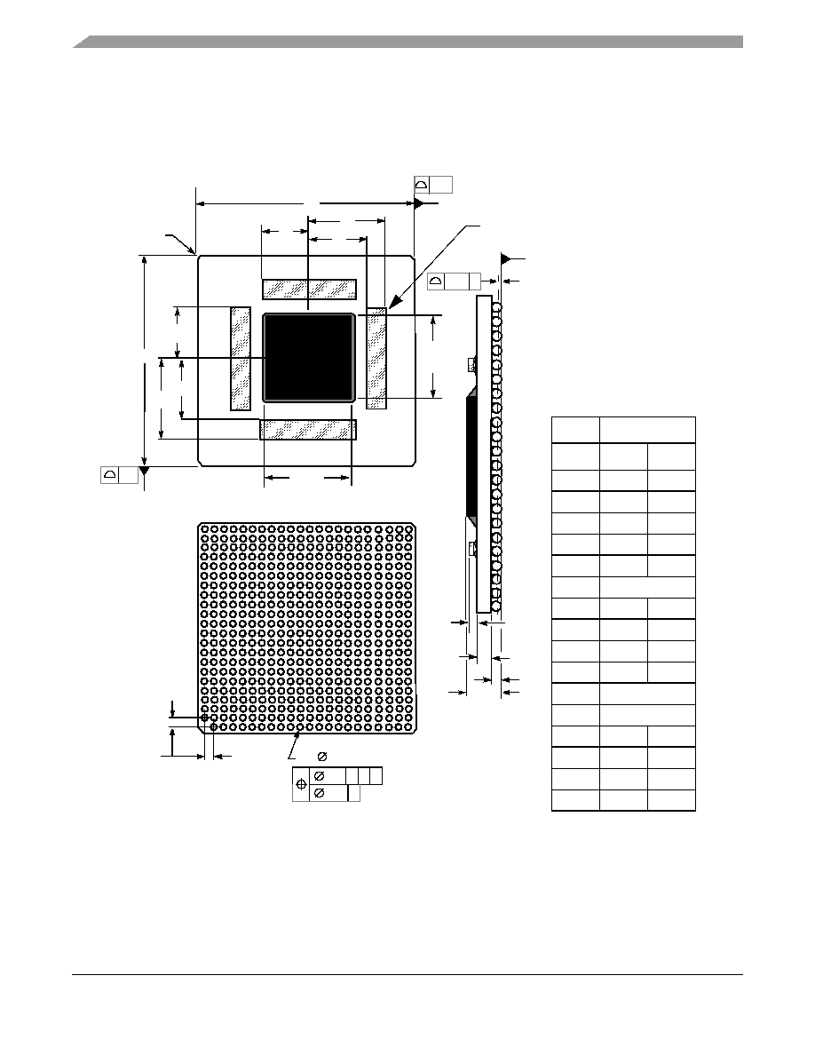
MPC7455 RISC Microprocessor Hardware Specifications, Rev. 4.1
44
Freescale Semiconductor
Package Description
8.5 Mechanical Dimensions for the MPC7455, 483 CBGA
Figure 22
provides the mechanical dimensions and
bottom surface nomenclature for the MPC7455, 483 CBGA
package.
Figure 22. Mechanical Dimensions and Bottom Surface Nomenclature for the MPC7455,
483 CBGA Package
0.2
2X
NOTES:
1. DIMENSIONING AND TOLERANCING
PER ASME Y14.5M, 1994.
2. DIMENSIONS IN MILLIMETERS.
3. TOP SIDE A1 CORNER INDEX IS A
METALIZED FEATURE WITH VARIOUS
SHAPES. BOTTOM SIDE. A1 CORNER
IS DESIGNATED WITH A BALL
MISSING FROM THE ARRAY.
D
A1 CORNER
E
e
0.2
2X
C
B
1 2 3 4 5 6 7 8 9 10 11 1213141516
A
B
C
D
E
F
G
H
J
K
L
M
N
P
R
T
A
A1
A2
A
0.15 A
171819
U
W
V
Millimeters
DIM
MIN
MAX
A
2.72
3.20
A1
0.80
1.00
A2
1.10
1.30
A3
--
0.60
b
0.82
0.93
D
29.00 BSC
D1
--
11.6
D2
8.94
--
D3
--
7.1
D4
12.15
12.45
e
1.27 BSC
E
29.00 BSC
E1
--
11.6
E2
8.94
--
E3
--
6.9
E4
8.75
9.20
C
A
483X
B
0.3
A
0.15
b
2021 22
Y
AA
AB
Capacitor Region
1
D1
D3
E1
E3
D2
E2
A3
D4
E4

MPC7455 RISC Microprocessor Hardware Specifications, Rev. 4.1
Freescale Semiconductor
45
System Design Information
8.6 Substrate Capacitors for the MPC7455, 483 CBGA
Figure 23
shows the connectivity of the substrate capacitor pads for the MPC7455, 483 CBGA. All capacitors are
100 nF.
Figure 23. Substrate Bypass Capacitors for the MPC7455, 483 CBGA
9
System Design Information
This section provides system and thermal design recommendations for successful application of the MPC7455.
9.1 PLL Configuration
The MPC7455 PLL is configured by the PLL_CFG[0:4] signals. For a given SYSCLK (bus) frequency, the PLL
configuration signals set the internal CPU and VCO frequency of operation. The PLL configuration for the
MPC7455 is shown in
Table 17
for a set of example frequencies. In this example, shaded cells represent settings
that, for a given SYSCLK frequency, result in core and/or VCO frequencies that do not comply with the 1-GHz
column in
Table 8
. Note that these configurations were different in devices prior to Rev F; see
Section 11.2, "Part
Numbers Not Fully Addressed by This Document
,"
for more information regarding documentation of prior
revisions.
Capacitor
Pad Number
-1
-2
C1
OV
DD
GND
C2
V
DD
GND
C3
OV
DD
GND
C4
OV
DD
GND
C5
V
DD
GND
C6
OV
DD
GND
C7
AV
DD
GND
C8
OV
DD
GND
C9
GV
DD
GND
C10
GV
DD
GND
C11
V
DD
GND
C12
GV
DD
GND
1
C3-1
C3-2
C2-2
C1-2
C1-1
C2-1
A1 Corner
C7-2
C7-1
C8-1
C9-1
C9-2
C8-2
C12
-
1
C12
-
2
C
1
1
-
2
C1
0-
2
C1
0-
1
C1
1-
1
C4-
2
C4-
1
C5-
1
C6-
1
C6-
2
C5-
2

MPC7455 RISC Microprocessor Hardware Specifications, Rev. 4.1
46
Freescale Semiconductor
System Design Information
Table 17. MPC7455 Microprocessor PLL Configuration Example for 1.0 GHz Parts
PLL_
CFG[0:4]
Example Bus-to-Core Frequency in MHz (VCO Frequency in MHz)
Bus-to-
Core
Multiplier
Core-to-
VCO
Multiplier
Bus (SYSCLK) Frequency
33.3
MHz
50
MHz
66.6
MHz
75
MHz
83
MHz
100
MHz
133
MHz
01000
2x
2x
10000 3x
2x
10100 4x
2x
532
(1064)
10110
5x
2x
500
(1000)
667
(1333)
10010
5.5x
2x
550
(1100)
733
(1466)
11010
6x
2x
600
(1200)
800
(1600)
01010
6.5x
2x
540
(1080)
650
(1300)
866
(1730)
00100
7x
2x
525
(1050)
580
(1160)
700
(1400)
931
(1862)
00010
7.5x
2x
500
(1000)
563
(1125)
623
(1245)
750
(1500)
1000
(2000)
11000
8x
2x
533
(1066)
600
(1200)
664
(1328)
800
(1600)
01100
8.5x
2x
566
(1132)
638
(1276)
706
(1412)
850
(1700)
01111
9x
2x
600
(1200)
675
(1350)
747
(1494)
900
(1800)
01110
9.5x
2x
633
(1266)
712
(1524)
789
(1578)
950
(1900)
10101
10x
2x
500
(1000)
667
(1333)
750
(1500)
830
(1660)
1000
(2000)
10001
10.5x
2x
525
(1050)
700
(1400)
938
(1876)
872
(1744)
10011
11x
2x
550
(1100)
733
(1466)
825
(1650)
913
(1826)
00000
11.5x
2x
575
(1150)
766
(532)
863
(1726)
955
(1910)
10111
12x
2x
600
(1200)
800
(1600)
900
(1800)
996
(1992)
MPC7455 RISC Microprocessor Hardware Specifications, Rev. 4.1
Freescale Semiconductor
47
System Design Information
11111
12.5x
2x
600
(1200)
833
(1666)
938
(1876)
01011
13x
2x
650
(1300)
865
(1730)
975
(1950)
11100
13.5x
2x
675
(1350)
900
(1800)
11001
14x
2x
700
(1400)
933
(1866)
00011
15x
2x
500
(1000)
750
(1500)
1000
(2000)
11011
16x
2x
533
(1066)
800
(1600)
00001
17x
2x
566
(1132)
850
(1900)
00101
18x
2x
600
(1200)
900
(1800)
00111
20x
2x
667
(1334)
1000
(2000)
01001
21x
2x
700
(1400)
01101
24x
2x
800
(1600)
11101
28x
2x
933
(1866)
00110
PLL bypass
PLL off, SYSCLK clocks core circuitry directly
11110
PLL off
PLL off, no core clocking occurs
Notes:
1. PLL_CFG[0:4] settings not listed are reserved.
2. The sample bus-to-core frequencies shown are for reference only. Some PLL configurations may select bus, core,
or VCO frequencies which are not useful, not supported, or not tested for by the MPC7455; see
Section 5.2.1,
"Clock AC Specifications
," for valid SYSCLK, core, and VCO frequencies.
3. In PLL-bypass mode, the SYSCLK input signal clocks the internal processor directly and the PLL is disabled.
However, the bus interface unit requires a 2x clock to function. Therefore, an additional signal, EXT_QUAL, must
be driven at one-half the frequency of SYSCLK and offset in phase to meet the required input setup t
IVKH
and hold
time t
IXKH
(see
Table 9
). The result will be that the processor bus frequency will be one-half SYSCLK while the
internal processor is clocked at SYSCLK frequency. This mode is intended for factory use and emulator tool use
only.
Note: The AC timing specifications given in this document do not apply in PLL-bypass mode.
4. In PLL-off mode, no clocking occurs inside the MPC7455 regardless of the SYSCLK input.
Table 17. MPC7455 Microprocessor PLL Configuration Example for 1.0 GHz Parts (continued)
PLL_
CFG[0:4]
Example Bus-to-Core Frequency in MHz (VCO Frequency in MHz)
Bus-to-
Core
Multiplier
Core-to-
VCO
Multiplier
Bus (SYSCLK) Frequency
33.3
MHz
50
MHz
66.6
MHz
75
MHz
83
MHz
100
MHz
133
MHz
MPC7455 RISC Microprocessor Hardware Specifications, Rev. 4.1
48
Freescale Semiconductor
System Design Information
The MPC7455 generates the clock for the external L3 synchronous data SRAMs by dividing the core clock
frequency of the MPC7455. The core-to-L3 frequency divisor for the L3 PLL is selected through the L3_CLK bits
of the L3CR register. Generally, the divisor must be chosen according to the frequency supported by the external
RAMs, the frequency of the MPC7455 core, and timing analysis of the circuit board routing.
Table 18
shows various
example L3 clock frequencies that can be obtained for a given set of core frequencies.
9.2 PLL Power Supply Filtering
The AV
DD
power signal is provided on the MPC7455 to provide power to the clock generation PLL. To ensure
stability of the internal clock, the power supplied to the AV
DD
input signal should be filtered of any noise in the 500
kHz to 10 MHz resonant frequency range of the PLL. A circuit similar to the one shown in
Figure 24
using surface
mount capacitors with minimum effective series inductance (ESL) is recommended.
The circuit should be placed as close as possible to the AV
DD
pin to minimize noise coupled from nearby circuits.
It is often possible to route directly from the capacitors to the AV
DD
pin, which is on the periphery of the 360 CBGA
footprint and very close to the periphery of the 483 CBGA footprint, without the inductance of vias.
Table 18. Sample Core-to-L3 Frequencies
Core Frequency
(MHz)
�2
�2.5
�3
�3.5
�4
�5
�6
500
250
200
167
143
125
100
83
533
266
213
178
152
133
107
89
550
275
220
183
157
138
110
92
600
300
240
200
171
150
120
100
650
2
325
260
217
186
163
130
108
666
2
333
266
222
190
167
133
111
700
2
350
280
233
200
175
140
117
733
2
367
293
244
209
183
147
122
800
2
400
320
266
230
200
160
133
867
2
433
347
289
248
217
173
145
933
2
467
373
311
266
233
187
156
1000
2
500
400
333
285
250
200
166
Notes:
1. The core and L3 frequencies are for reference only. Note that maximum L3 frequency is design dependent. Some
examples may represent core or L3 frequencies which are not useful, not supported, or not tested for the MPC7455;
see
Section 5.2.3, "L3 Clock AC Specifications,"
for valid L3_CLK frequencies and for more information regarding
the maximum L3 frequency. Shaded cells do not comply with
Table 10
.
2. These core frequencies are not supported by all speed grades; see
Table 8
.
MPC7455 RISC Microprocessor Hardware Specifications, Rev. 4.1
Freescale Semiconductor
49
System Design Information
Figure 24. PLL Power Supply Filter Circuit
9.3 Decoupling Recommendations
Due to the MPC7455 dynamic power management feature, large address and data buses, and high operating
frequencies, the MPC7455 can generate transient power surges and high frequency noise in its power supply,
especially while driving large capacitive loads. This noise must be prevented from reaching other components in the
MPC7455 system, and the MPC7455 itself requires a clean, tightly regulated source of power. Therefore, it is
recommended that the system designer place at least one decoupling capacitor at each V
DD
, OV
DD
, and GV
DD
pin
of the MPC7455. It is also recommended that these decoupling capacitors receive their power from separate V
DD
,
OV
DD
/GV
DD
, and GND power planes in the PCB, utilizing short traces to minimize inductance.
These capacitors should have a value of 0.01 or 0.1 �F. Only ceramic surface mount technology (SMT) capacitors
should be used to minimize lead inductance, preferably 0508 or 0603 orientations where connections are made along
the length of the part. Consistent with the recommendations of Dr. Howard Johnson in High Speed Digital Design:
A Handbook of Black Magic (Prentice Hall, 1993) and contrary to previous recommendations for decoupling
Freescale microprocessors, multiple small capacitors of equal value are recommended over using multiple values of
capacitance.
In addition, it is recommended that there be several bulk storage capacitors distributed around the PCB, feeding the
V
DD
, GV
DD
, and OV
DD
planes, to enable quick recharging of the smaller chip capacitors. These bulk capacitors
should have a low equivalent series resistance (ESR) rating to ensure the quick response time necessary. They should
also be connected to the power and ground planes through two vias to minimize inductance. Suggested bulk
capacitors: 100�330 � F (AVX TPS tantalum or Sanyo OSCON).
9.4 Connection Recommendations
To ensure reliable operation, it is highly recommended to connect unused inputs to an appropriate signal level.
Unused active low inputs should be tied to OV
DD
. Unused active high inputs should be connected to GND. All NC
(no-connect) signals must remain unconnected.
Power and ground connections must be made to all external V
DD
, OV
DD
, GV
DD
, and GND pins in the MPC7455.
If the L3 interface is not used, GV
DD
should be connected to the OV
DD
power plane, and L3VSEL should be
connected to BVSEL.
9.5 Output Buffer DC Impedance
The MPC7455 processor bus and L3 I/O drivers are characterized over process, voltage, and temperature. To
measure Z
0
, an external resistor is connected from the chip pad to OV
DD
or GND. Then, the value of each resistor
is varied until the pad voltage is OV
DD
/2 (see
Figure 25
).
The output impedance is the average of two components, the resistances of the pull-up and pull-down devices. When
data is held low, SW2 is closed (SW1 is open), and R
N
is trimmed until the voltage at the pad equals OV
DD
/2. R
N
then becomes the resistance of the pull-down devices. When data is held high, SW1 is closed (SW2 is open), and
V
DD
AV
DD
10
2.2 �F
2.2 �F
GND
Low ESL Surface Mount Capacitors
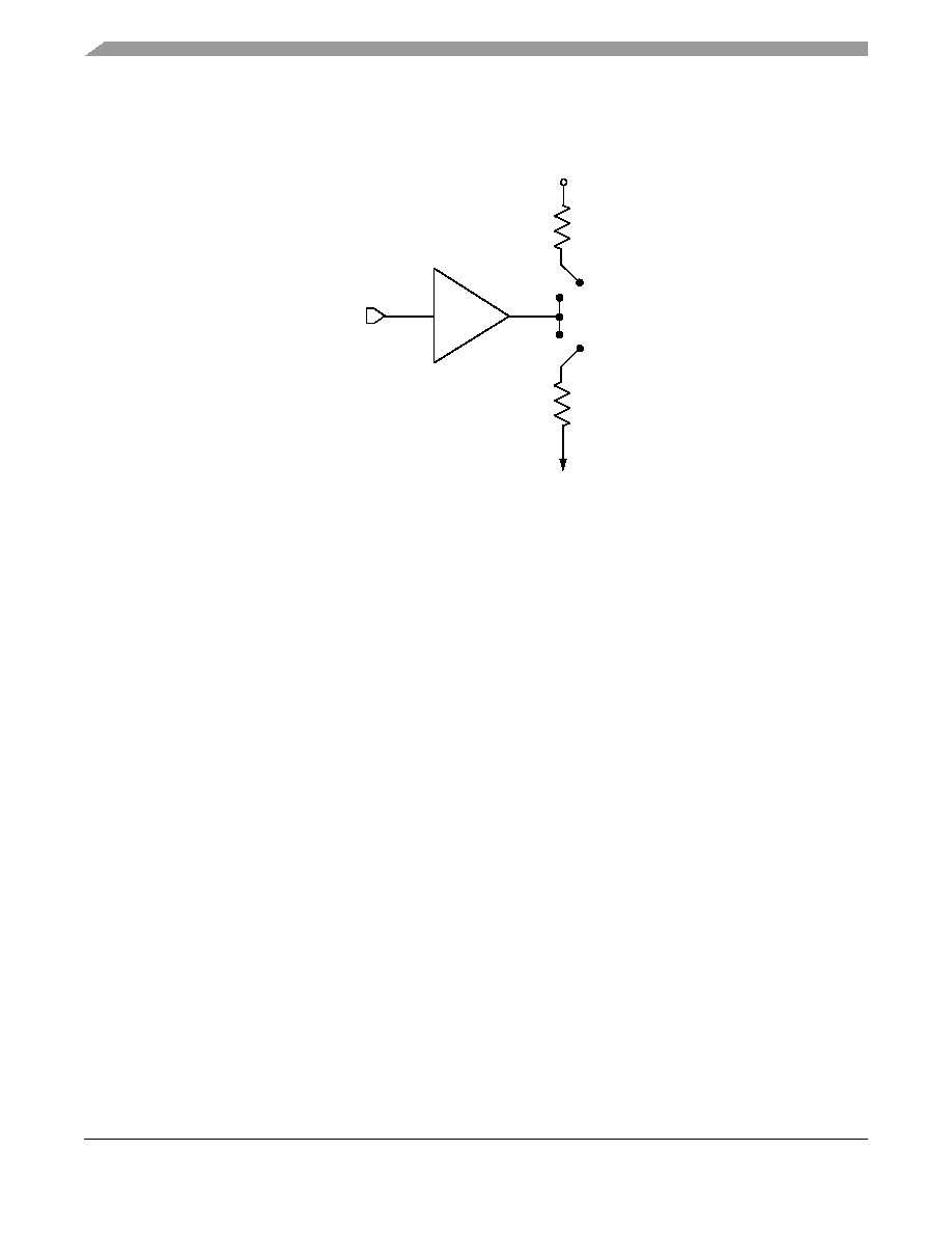
MPC7455 RISC Microprocessor Hardware Specifications, Rev. 4.1
50
Freescale Semiconductor
System Design Information
R
P
is trimmed until the voltage at the pad equals OV
DD
/2. R
P
then becomes the resistance of the pull-up devices. R
P
and R
N
are designed to be close to each other in value. Then, Z
0
= (R
P
+ R
N
)/2.
Figure 25. Driver Impedance Measurement
OV
DD
OGND
R
P
R
N
Pad
Data
SW1
SW2

MPC7455 RISC Microprocessor Hardware Specifications, Rev. 4.1
Freescale Semiconductor
51
System Design Information
Table 19
summarizes the signal impedance results. The impedance increases with junction temperature and is
relatively unaffected by bus voltage.
9.6 Pull-Up/Pull-Down Resistor Requirements
The MPC7455 requires high-resistive (weak: 4.7-k
) pull-up resistors on several control pins of the bus interface
to maintain the control signals in the negated state after they have been actively negated and released by the
MPC7455 or other bus masters. These pins are: TS, ARTRY, SHDO, and SHD1.
Some pins designated as being for factory test must be pulled up to OV
DD
or down to GND to ensure proper device
operation. For the MPC7445, 360 BGA, the pins that must be pulled up to OV
DD
are: LSSD_MODE and TEST[0:3];
the pins that must be pulled down to GND are: L1_TSTCLK and TEST[4]. For the MPC7455, 483 BGA, the pins
that must be pulled up to OV
DD
are: LSSD_MODE and TEST[0:5]; the pins that must be pulled down are:
L1_TSTCLK and TEST[6]. The CKSTP_IN signal should likewise, be pulled up through a pull-up resistor (weak
or stronger: 4.7�1 k
) to prevent erroneous assertions of this signal
In addition, the MPC7455 has one open-drain style output that requires a pull-up resistor (weak or stronger:
4.7�1 k
) if it is used by the system. This pin is CKSTP_OUT.
If pull-down resistors are used to configure BVSEL or L3VSEL, the resistors should be less than 250
(see
Table 16
). Because PLL_CFG[0:4] must remain stable during normal operation, strong pull-up and pull-down
resistors (1 k
or less) are recommended to configure these signals in order to protect against erroneous switching
due to ground bounce, power supply noise or noise coupling.
During inactive periods on the bus, the address and transfer attributes may not be driven by any master and may,
therefore, float in the high-impedance state for relatively long periods of time. Because the MPC7455 must
continually monitor these signals for snooping, this float condition may cause excessive power draw by the input
receivers on the MPC7455 or by other receivers in the system. These signals can be pulled up through weak (10-k
)
pull-up resistors by the system, address bus driven mode enabled (see the MPC7450 RISC Microporcessor Family
Users' Manual for more information on this mode), or they may be otherwise driven by the system during inactive
periods of the bus to avoid this additional power draw. Preliminary studies have shown the additional power draw
by the MPC7455 input receivers to be negligible and, in any event, none of these measures are necessary for proper
device operation. The snooped address and transfer attribute inputs are: A[0:35], AP[0:4], TT[0:4], CI, WT, and
GBL.
If extended addressing is not used, A[0:3] are unused and must be pulled low to GND through weak pull-down
resistors. If the MPC7455 is in 60x bus mode, DTI[0:3] must be pulled low to GND through weak pull-down
resistors.
The data bus input receivers are normally turned off when no read operation is in progress and, therefore, do not
require pull-up resistors on the bus. Other data bus receivers in the system, however, may require pull-ups, or that
those signals be otherwise driven by the system during inactive periods by the system. The data bus signals are:
D[0:63] and DP[0:7].
Table 19. Impedance Characteristics
V
DD
= 1.5 V, OV
DD
= 1.8 V � 5%, T
j
= 5��85�C
Impedance
Processor Bus
L3 Bus
Unit
Z
0
Typical
33�42
34�42
Maximum
31�51
32�44

MPC7455 RISC Microprocessor Hardware Specifications, Rev. 4.1
52
Freescale Semiconductor
System Design Information
If address or data parity is not used by the system, and the respective parity checking is disabled through HID0, the
input receivers for those pins are disabled, and those pins do not require pull-up resistors and should be left
unconnected by the system. If all parity generation is disabled through HID0, then all parity checking should also
be disabled through HID0, and all parity pins may be left unconnected by the system.
The L3 interface does not normally require pull-up resistors.
9.7 JTAG Configuration Signals
Boundary-scan testing is enabled through the JTAG interface signals. The TRST signal is optional in the IEEE
1149.1 specification, but is provided on all processors that implement the PowerPC architecture. While it is possible
to force the TAP controller to the reset state using only the TCK and TMS signals, more reliable power-on reset
performance will be obtained if the TRST signal is asserted during power-on reset. Because the JTAG interface is
also used for accessing the common on-chip processor (COP) function, simply tying TRST to HRESET is not
practical.
The COP function of these processors allows a remote computer system (typically, a PC with dedicated hardware
and debugging software) to access and control the internal operations of the processor. The COP interface connects
primarily through the JTAG port of the processor, with some additional status monitoring signals. The COP port
requires the ability to independently assert HRESET or TRST in order to fully control the processor. If the target
system has independent reset sources, such as voltage monitors, watchdog timers, power supply failures, or
push-button switches, then the COP reset signals must be merged into these signals with logic.
The arrangement shown in
Figure 26
allows the COP port to independently assert HRESET or TRST, while ensuring
that the target can drive HRESET as well. If the JTAG interface and COP header will not be used, TRST should be
tied to HRESET through a 0-
isolation resistor so that it is asserted when the system reset signal (HRESET) is
asserted, ensuring that the JTAG scan chain is initialized during power-on. While Freescale recommends that the
COP header be designed into the system as shown in
Figure 26
, if this is not possible, the isolation resistor will allow
future access to TRST in the case where a JTAG interface may need to be wired onto the system in debug situations.
The COP header shown in
Figure 26
adds many benefits--breakpoints, watchpoints, register and memory
examination/modification, and other standard debugger features are possible through this interface--and can be as
inexpensive as an unpopulated footprint for a header to be added when needed.
The COP interface has a standard header for connection to the target system, based on the 0.025" square-post, 0.100"
centered header assembly (often called a Berg header). The connector typically has pin 14 removed as a connector
key.
There is no standardized way to number the COP header shown in
Figure 26
; consequently, many different pin
numbers have been observed from emulator vendors. Some are numbered top-to-bottom then left-to-right, while
others use left-to-right then top-to-bottom, while still others number the pins counter clockwise from pin 1 (as with
an IC). Regardless of the numbering, the signal placement recommended in
Figure 26
is common to all known
emulators.
The QACK signal shown in
Figure 26
is usually connected to the PCI bridge chip in a system and is an input to the
MPC7455 informing it that it can go into the quiescent state. Under normal operation this occurs during a low-power
mode selection. In order for COP to work, the MPC7455 must see this signal asserted (pulled down). While shown
on the COP header, not all emulator products drive this signal. If the product does not, a pull-down resistor can be
populated to assert this signal. Additionally, some emulator products implement open-drain type outputs and can
only drive QACK asserted; for these tools, a pull-up resistor can be implemented to ensure this signal is de-asserted
when it is not being driven by the tool. Note that the pull-up and pull-down resistors on the QACK signal are
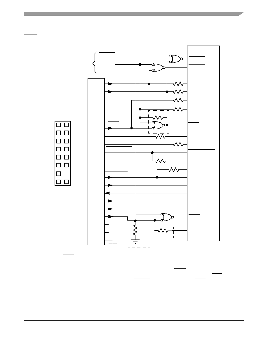
MPC7455 RISC Microprocessor Hardware Specifications, Rev. 4.1
Freescale Semiconductor
53
System Design Information
mutually exclusive and it is never necessary to populate both in a system. To preserve correct power-down operation,
QACK should be merged via logic so that it also can be driven by the PCI bridge.
Figure 26. JTAG Interface Connection
HRESET
HRESET
From Target
Board Sources
HRESET
13
SRESET
SRESET
SRESET
NC
NC
11
VDD_SENSE
6
5
1
15
2 k
10 k
10 k
10 k
OV
DD
OV
DD
OV
DD
OV
DD
CHKSTP_IN
CHKSTP_IN
8
TMS
TDO
TDI
TCK
TMS
TDO
TDI
TCK
9
1
3
4
TRST
7
16
2
10
12
(if any)
CO
P Head
er
14
2
Key
QACK
OV
DD
OV
DD
10 k
OV
DD
TRST
10 k
OV
DD
10 k
10 k
QACK
QACK
CHKSTP_OUT
CHKSTP_OUT
3
13
9
5
1
6
10
2
15
11
7
16
12
8
4
KEY
No Pin
COP Connector
Physical Pin Out
10 k
4
OV
DD
1
2 k
3
0
5
Notes:
1. RUN/STOP, normally found on pin 5 of the COP header, is not implemented on the MPC7455. Con
pin 5 of the COP header to OV
DD
with a 10-k
pull-up resistor.
2. Key location; pin 14 is not physically present on the COP header.
3. Component not populated. Populate only if debug tool does not drive QACK.
4. Populate only if debug tool uses an open-drain type output and does not actively de-assert QACK
5. If the JTAG interface is implemented, connect HRESET from the target source to TRST from the
header though an AND gate to TRST of the part. If the JTAG interface is not implemented, con
HRESET from the target source to TRST of the part through a 0-
isolation reisistor.
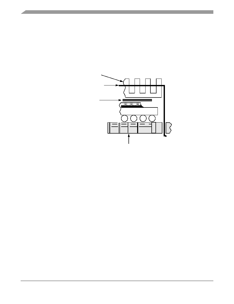
MPC7455 RISC Microprocessor Hardware Specifications, Rev. 4.1
54
Freescale Semiconductor
System Design Information
9.8 Thermal Management Information
This section provides thermal management information for the ceramic ball grid array (CBGA) package for
air-cooled applications. Proper thermal control design is primarily dependent on the system-level design--the heat
sink, airflow, and thermal interface material. To reduce the die-junction temperature, heat sinks may be attached to
the package by several methods--spring clip to holes in the printed-circuit board or package, and mounting clip and
screw assembly (see
Figure 27
); however, due to the potential large mass of the heat sink, attachment through the
printed-circuit board is suggested. If a spring clip is used, the spring force should not exceed 10 pounds.
Figure 27. Package Exploded Cross-Sectional View with Several Heat Sink Options
The board designer can choose between several types of heat sinks to place on the MPC7455. There are several
commercially available heat sinks for the MPC7455 provided by the following vendors:
Aavid Thermalloy
603-224-9988
80 Commercial St.
Concord, NH 03301
Internet: www.aavidthermalloy.com
Alpha Novatech
408-749-7601
473 Sapena Ct. #15
Santa Clara, CA 95054
Internet: www.alphanovatech.com
International Electronic Research Corporation (IERC)
818-842-7277
413 North Moss St.
Burbank, CA 91502
Internet: www.ctscorp.com
Tyco Electronics
800-522-6752
Chip CoolersTM
P.O. Box 3668
Harrisburg, PA 17105-3668
Internet: www.chipcoolers.com
Thermal Interface Material
Heat Sink
CBGA Package
Heat Sink
Clip
Printed-Circuit Board

MPC7455 RISC Microprocessor Hardware Specifications, Rev. 4.1
Freescale Semiconductor
55
System Design Information
Wakefield Engineering
603-635-5102
33 Bridge St.
Pelham, NH 03076
Internet: www.wakefield.com
Ultimately, the final selection of an appropriate heat sink depends on many factors, such as thermal performance at
a given air velocity, spatial volume, mass, attachment method, assembly, and cost.
9.8.1 Internal Package Conduction Resistance
For the exposed-die packaging technology, shown in
Table 3
, the intrinsic conduction thermal resistance paths are
as follows:
�
The die junction-to-case (actually top-of-die since silicon die is exposed) thermal resistance
�
The die junction-to-ball thermal resistance
Figure 28
depicts the primary heat transfer path for a package with an attached heat sink mounted to a printed-circuit
board.
Figure 28. C4 Package with Heat Sink Mounted to a Printed-Circuit Board
Heat generated on the active side of the chip is conducted through the silicon, then through the heat sink attach
material (or thermal interface material), and finally to the heat sink where it is removed by forced-air convection.
Because the silicon thermal resistance is quite small, for a first-order analysis, the temperature drop in the silicon
may be neglected. Thus, the thermal interface material and the heat sink conduction/convective thermal resistances
are the dominant terms.
9.8.2 Thermal Interface Materials
A thermal interface material is recommended at the package lid-to-heat sink interface to minimize the thermal
contact resistance. For those applications where the heat sink is attached by spring clip mechanism,
Figure 29
shows
the thermal performance of three thin-sheet thermal-interface materials (silicone, graphite/oil, floroether oil), a bare
joint, and a joint with thermal grease as a function of contact pressure. As shown, the performance of these thermal
interface materials improves with increasing contact pressure. The use of thermal grease significantly reduces the
External Resistance
External Resistance
Internal Resistance
Radiation
Convection
Radiation
Convection
Heat Sink
Printed-Circuit Board
Thermal Interface Material
Package/Leads
Die Junction
Die/Package
(Note the internal versus external package resistance.)
MPC7455 RISC Microprocessor Hardware Specifications, Rev. 4.1
56
Freescale Semiconductor
System Design Information
interface thermal resistance. That is, the bare joint results in a thermal resistance approximately seven times greater
than the thermal grease joint.
Often, heat sinks are attached to the package by means of a spring clip to holes in the printed-circuit board (see
Figure 27
). Therefore, the synthetic grease offers the best thermal performance, considering the low interface
pressure and is recommended due to the high power dissipation of the MPC7455. Of course, the selection of any
thermal interface material depends on many factors--thermal performance requirements, manufacturability, service
temperature, dielectric properties, cost, etc.
Figure 29. Thermal Performance of Select Thermal Interface Material
The board designer can choose between several types of thermal interface. Heat sink adhesive materials should be
selected based on high conductivity, yet adequate mechanical strength to meet equipment shock/vibration
requirements. There are several commercially available thermal interfaces and adhesive materials provided by the
following vendors:
The Bergquist Company
800-347-4572
18930 West 78
th
St.
Chanhassen, MN 55317
Internet: www.bergquistcompany.com
Chomerics, Inc.
781-935-4850
77 Dragon Ct.
Woburn, MA 01888-4014
Internet: www.chomerics.com
0
0.5
1
1.5
2
0
10
20
30
40
50
60
70
80
Silicone Sheet (0.006 in.)
Bare Joint
Floroether Oil Sheet (0.007 in.)
Graphite/Oil Sheet (0.005 in.)
Synthetic Grease
Contact Pressure (psi)
S
peci
f
i
c
The
r
m
a
l
Re
si
st
anc
e (
K
-
i
n.
2
/W
)

MPC7455 RISC Microprocessor Hardware Specifications, Rev. 4.1
Freescale Semiconductor
57
System Design Information
Dow-Corning Corporation
800-248-2481
Dow-Corning Electronic Materials
2200 W. Salzburg Rd.
Midland, MI 48686-0997
Internet: www.dow.com
Shin-Etsu MicroSi, Inc.
888-642-7674
10028 S. 51st St.
Phoenix, AZ 85044
Internet: www.microsi.com
Thermagon Inc.
888-246-9050
4707 Detroit Ave.
Cleveland, OH 44102
Internet: www.thermagon.com
The following section provides a heat sink selection example using one of the commercially available heat sinks.
9.8.3 Heat Sink Selection Example
For preliminary heat sink sizing, the die-junction temperature can be expressed as follows:
T
j
= T
a
+ T
r
+ (R
JC
+ R
int
+ R
sa
)
� P
d
where:
T
j
is the die-junction temperature
T
a
is the inlet cabinet ambient temperature
T
r
is the air temperature rise within the computer cabinet
R
JC
is the junction-to-case thermal resistance
R
int
is the adhesive or interface material thermal resistance
R
sa
is the heat sink base-to-ambient thermal resistance
P
d
is the power dissipated by the device
During operation, the die-junction temperatures (T
j
) should be maintained less than the value specified in
Table 4
.
The temperature of air cooling the component greatly depends on the ambient inlet air temperature and the air
temperature rise within the electronic cabinet. An electronic cabinet inlet-air temperature (T
a
) may range from 30�
to 40�C. The air temperature rise within a cabinet (T
r
) may be in the range of 5� to 10�C. The thermal resistance of
the thermal interface material (R
int
) is typically about 1.5�C/W. For example, assuming a T
a
of 30�C, a T
r
of 5�C,
a CBGA package R
JC
= 0.1, and a typical power consumption (P
d
) of 15.0 W, the following expression for T
j
is
obtained:
Die-junction temperature:
T
j
= 30�C + 5�C + (0.1�C/W + 1.5�C/W + R
sa
)
� 15 W
For this example, a R
sa
value of 3.1�C/W or less is required to maintain the die-junction temperature below the
maximum value of
Table 4
.
Though the die junction-to-ambient and the heat sink-to-ambient thermal resistances are a common figure-of-merit
used for comparing the thermal performance of various microelectronic packaging technologies, one should
exercise caution when only using this metric in determining thermal management because no single parameter can
adequately describe three-dimensional heat flow. The final die-junction operating temperature is not only a function
of the component-level thermal resistance, but the system-level design and its operating conditions. In addition to
the component's power consumption, a number of factors affect the final operating die-junction
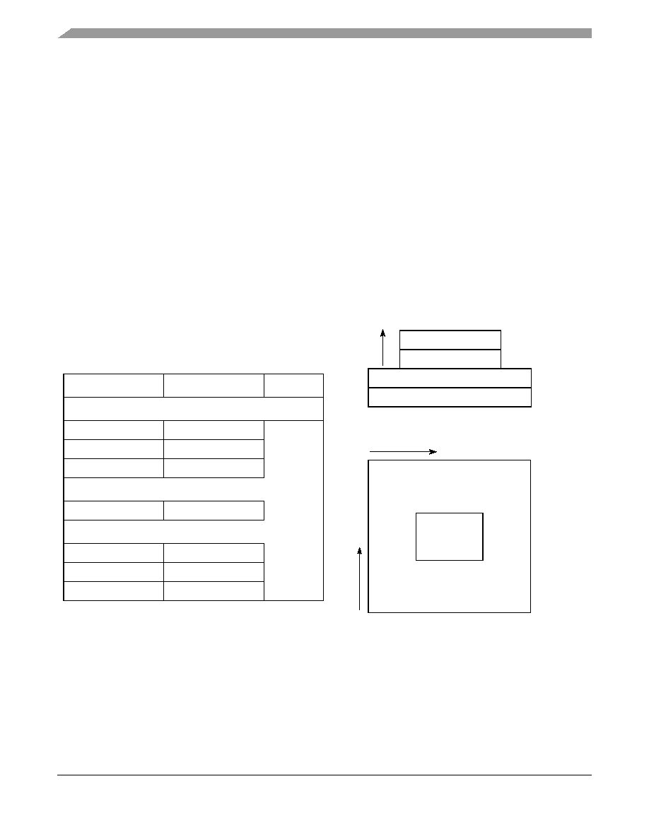
MPC7455 RISC Microprocessor Hardware Specifications, Rev. 4.1
58
Freescale Semiconductor
System Design Information
temperature--airflow, board population (local heat flux of adjacent components), heat sink efficiency, heat sink
attach, heat sink placement, next-level interconnect technology, system air temperature rise, altitude, etc.
Due to the complexity and the many variations of system-level boundary conditions for today's microelectronic
equipment, the combined effects of the heat transfer mechanisms (radiation, convection, and conduction) may vary
widely. For these reasons, we recommend using conjugate heat transfer models for the board, as well as system-level
designs.
For system thermal modeling, the MPC7445 and MPC7455 thermal model is shown in
Figure 30
. Four volumes will
be used to represent this device. Two of the volumes, solder ball, and air and substrate, are modeled using the
package outline size of the package. The other two, die, and bump and underfill, have the same size as the die.
Dimensions for these volumes for the MPC7445 and MPC7455 are given in
Figure 20
and
Figure 22
, respectively.
The silicon die should be modeled 9.10
� 12.25 � 0.74 mm with the heat source applied as a uniform source at the
bottom of the volume. The bump and underfill layer is modeled as 9.10
� 12.25 � 0.069 mm (or as a collapsed
volume) with orthotropic material properties: 0.6 W/(m � K) in the xy-plane and 2 W/(m � K) in the direction of the
z-axis. The substrate volume is 25
� 25 � 1.2 mm (MPC7445) or 29 � 29 � 1.2 mm (MPC7455), and this volume
has 18 W/(m � K) isotropic conductivity. The solder ball and air layer is modeled with the same horizontal
dimensions as the substrate and is 0.9 mm thick. It can also be modeled as a collapsed volume using orthotropic
material properties: 0.034 W/(m � K) in the xy-plane direction and 3.8 W/(m � K) in the direction of the z-axis.
Figure 30. Recommended Thermal Model of MPC7445 and MPC7455
Bump and Underfill
Die
Substrate
Solder and Air
Die
Substrate
Side View of Model (Not to Scale)
Top View of Model (Not to Scale)
x
y
z
Conductivity
Value
Unit
Bump and Underfill
k
x
0.6
W/(m � K)
k
y
0.6
k
z
2
Substrate
k
18
Solder Ball and Air
k
x
0.034
k
y
0.034
k
z
3.8
MPC7455 RISC Microprocessor Hardware Specifications, Rev. 4.1
Freescale Semiconductor
59
Document Revision History
10 Document Revision History
Table 20
provides a revision history for this hardware specification.
Table 20. Document Revision History
Rev. No.
Substantive Change(s)
0
Initial release.
1
Updated for Rev F devices; information specific to Rev C devices is now documented in a separate part
number specifications; see
Section 11.2, "Part Numbers Not Fully Addressed by This Document,"
for
more information.
Removed 600 and 800 MHz speed grades.
Increased leakage current specifications in
Table 6
from 10 to 30 �A.
Changed core voltage to 1.3 V; all instances of V
DD
and AV
DD
updated.
Updated power consumption specifications in
Table 7
.
Reduced I/O power guidance in
Table 7
from <20% to <5%.
Added footnote 1 to
Figure 9
and
Figure 11
.
Removed CI and WT from Input Setup and Input Hold lists in
Table 10
; these are output-only signals.
Removed INT, HRESET, MCP, SRESET, and SMI from Input Setup and Input Hold lists in
Table 10
;
these are asynchronous inputs.
Added TT[0:3] to Input Setup, Input Hold, Output Valid, and Output Hold lists in
Table 10
; these were
mistakenly omitted in Rev 0.
Updated
Table 13
and
Table 14
to reflect new L3 AC timing in Rev F devices.
Corrected Note 10 in
Table 16
and
Table 17
; this is an event pin, not an enable pin.
Corrected entries for L3_ECHO_CLK[1,3] in
Table 17
; these are I/O pins, not input-only.
Added Note 16 to
Table 17
; all No Connect pins must be left unconnected.
Changed name of PLL_EXT to PLL_CFG[4] and updated all instances.
Updated
Table 18
to reflect PLL configuration settings for Rev F devices.
Added dimensions D2 and E3 to
Figure 20
.
Transposed dimensions D4 and E4 in
Figure 21
(dimensions were reversed).
Revised
Figure 24
and
Section 9.7, "JTAG Configuration Signals."
Revised format of
Section 11.2, "Part Numbers Not Fully Addressed by This Document,"
and added
Table 23
through Table 26.
Revised
Section 9.8.3, "Heat Sink Selection Example,"
and added additional thermal modeling
information, including
Figure 28
.
Changed maximum heat sink clip spring force in
Section 9.8, "Thermal Management Information,"
from
5.5 lbs to 10 lbs.
Changed substrate marking for MPC7445 in
Figure 29
; all MPC744x device substrates are marked
MPC7440.
Changed substrate marking for MPC7455 in
Figure 29
; all MPC745x device substrates are marked
MPC7450.

MPC7455 RISC Microprocessor Hardware Specifications, Rev. 4.1
60
Freescale Semiconductor
Ordering Information
11 Ordering Information
Ordering information for the parts fully covered by this specification document is provided in
Section 11.1, "Part
Numbers Fully Addressed by This Document."
Note that the individual part numbers correspond to a maximum
processor core frequency. For available frequencies, contact your local Freescale sales office. In addition to the
processor frequency, the part numbering scheme also includes an application modifier which may specify special
application conditions. Each part number also contains a revision level code which refers to the die mask revision
number.
Section 11.2, "Part Numbers Not Fully Addressed by This Document,"
lists the part numbers which do not
1.1
Removed reference to Note 4 for DTI signals in
Table 15
and
Table 16
: these signals are unused in 60x
bus mode and must be pulled down (see Note 13); they are not ignored.
Improved precision of die and package dimensions in
Figure 20
and
Figure 21
.
2
Corrected entries in
Table 17
for 33 MHz and 50 MHz bus frequencies with multipliers of 24x and higher.
Corrected typographical errors in heatsink selection example in
Section 9.8.3, "Heat Sink Selection
Example."
Removed erroneous instances of PLL_EXT signal name and changed remaining instances of
PLL_CFG[0:3] to PLL_CFG[0:4]. (These were artifacts from older revisions; see entry for Rev 1.0.)
Corrected erroneous instances (artifacts) mentioning 1.6 V core voltage. Core voltage for devices
completely covered by this revision (and revisions 1.
x) of this document is 1.3 V.
Corrected errors in PLL multipliers in
Table 17
: 32x and 25x are not supported ratios, 3x and 4x are
supported, 10.5x and 12.5x PLL settings were incorrect.
Replaced notes at bottom of
Table 17
(erroneously missing in revisions 1.
x).
Updated coplanarity specifications in
Figure 20
and
Figure 21
from 0.2 mm to 0.15 mm.
3
Added Revision G (Rev 3.4) devices to specifications.
Added new PowerPC trademarking information.
4
Added substrate capacitor information in
Section 8.3, "Substrate Capacitors for the MPC7445, 360
CBGA,"
and
Section 8.6, "Substrate Capacitors for the MPC7455, 483 CBGA."
Clarified maximum and typical L3 clock frequency in
Section 5.2.3, "L3 Clock AC Specifications"
; typical
L3 frequency now stated as 250 MHz based on changes to L3 AC timing.
Significantly changed L3 AC timing in
Table 12
and
Table 13
. These changes reflect both updates
based on latest characterization and error corrections (effects of non-zero L3OH values were incorrectly
documented in earlier revisions of this document).
Clarified address bus pull-up resistor recommendations in
Section 9.6, "Pull-Up/Pull-Down Resistor
Requirements."
Added pull-up/pull-down recommendations for CKSTP_IN and PLL_CFG[0:4] to
Section 9.6,
"Pull-Up/Pull-Down Resistor Requirements."
Modified
Table 9
,
Figure 5
, and
Figure 6
to more accurately show when the mode select inputs
(BMODE[0:1], L3VSEL, BVSEL) are sampled and AC timing requirements.
Figure 20
and
Figure 22
: Updated/corrected dimensions in mechanical drawings.
4.1
Document tempate update.
Table 20. Document Revision History (continued)
Rev. No.
Substantive Change(s)
MPC7455 RISC Microprocessor Hardware Specifications, Rev. 4.1
Freescale Semiconductor
61
Ordering Information
fully conform to the specifications of this document. These special part numbers require an additional document
called a part number specification.
11.1 Part Numbers Fully Addressed by This Document
Table 21
provides the Freescale part numbering nomenclature for the MPC7455.
11.2 Part Numbers Not Fully Addressed by This Document
Parts with application modifiers or revision levels not fully addressed in this specification document are described
in separate part number specifications which supplement and supersede this document; see
Table 22
through
Table 25
.
Table 21. Part Numbering Nomenclature
xx
74
x5
x
RX
nnnn
x
x
Product
Code
Part
Identifier
Process
Descriptor
Package
Processor
Frequency
1
Application
Modifier
Revision Level
XC
2
7455
7445
A
RX = CBGA
733
867
933
1000
L: 1.3 V � 50 mV
0 to 105
�C
F: 3.3; PVR = 8001 0303
MC
G: 3.4; PVR = 8001 0304
Notes:
1. Processor core frequencies supported by parts addressed by this specification only. Parts addressed by part
number specifications may support other maximum core frequencies.
2. The X prefix in a Freescale part number designates a "Pilot Production Prototype" as defined by Freescale SOP
3-13. These are from a limited production volume of prototypes manufactured, tested, and Q.A. inspected on a
qualified technology to simulate normal production. These parts have only preliminary reliability and
characterization data. Before pilot production prototypes may be shipped, written authorization from the customer
must be on file in the applicable sales office acknowledging the qualification status and the fact that product changes
may still occur while shipping pilot production prototypes.
Table 22. Part Numbers Addressed by XPC74
x
5RX
nnn
LC Series Part Number Specification (Document
Order No. MPC7455RXLCPNS)
XPC
74
x5
RX
nnn
L
C
Product
Code
Part
Identifier
Package
Processor
Frequency
Application Modifier
Revision Level
XPC
7455
7445
RX = CBGA
600
733
800
867
933
L: 1.6 V � 50 mV
0 to 105
�C
C: 2.1; PVR = 8001 0201
PPC
1000

MPC7455 RISC Microprocessor Hardware Specifications, Rev. 4.1
62
Freescale Semiconductor
Ordering Information
11.3 Part Marking
Parts are marked as the example shown in
Figure 31
.
Figure 31. Part Marking for BGA Device
Table 23. Part Numbers Addressed by XPC74
x
5RX
nnn
N
x
Series Part Number Specification (Document
Order No. MPC7455RXNXPNS)
XPC
74
x5
RX
nnn
N
C
Product
Code
Part
Identifier
Package
Processor
Frequency
Application Modifier
Revision Level
XPC
7455
7445
RX = CBGA
600
733
800
N: 1.3 V � 50 mV
0 to 105
�C
C: 2.1; PVR = 8001 0201
Table 24. Part Numbers Addressed by XPC74
x
5RX
nnn
P
x
Series Part Number Specification (Document
Order No. MPC7455RXPXPNS)
XPC
7455
RX
nnn
P
C
Product
Code
Part
Identifier
Package
Processor
Frequency
Application Modifier
Revision Level
XPC
7455
RX = CBGA
933
1000
P: 1.85 V � 50 mV
0 to 65
�C
C: 2.1; PVR = 8001 0201
Table 25. Part Numbers Addressed by XPC74
x
5RX
nnn
S
x
Series Part Number Specification (Document
Order No. MPC7455RXSXPNS)
XPC
7455
RX
nnnn
S
C
Product
Code
Part
Identifier
Package
Processor
Frequency
Application Modifier
Revision Level
XPC
7455
RX = CBGA
1000
S: 1.85 V � 50 mV
0 to 75
�C
C: 2.1; PVR = 8001 0201
BGA
Notes
:
MMMMMM is the 6-digit mask number.
ATWLYYWWA is the traceability code.
MC7455A
RX1000LG
MMMMMM
ATWLYYWWA
7450
BGA
MC7445A
RX1000LG
MMMMMM
ATWLYYWWA
7440

MPC7455 RISC Microprocessor Hardware Specifications, Rev. 4.1
Freescale Semiconductor
63
Ordering Information
THIS PAGE INTENTIONALLY LEFT BLANK

MPC7455EC
Rev. 4.1
02/2005
FreescaleTM and the Freescale logo are trademarks of Freescale Semiconductor, Inc.
The described product is a PowerPC microprocessor. The PowerPC name is a
trademark of IBM Corp. and used under license. All other product or service names are
the property of their respective owners.
� Freescale Semiconductor, Inc. 2005.
Information in this document is provided solely to enable system and software
implementers to use Freescale Semiconductor products. There are no express or
implied copyright licenses granted hereunder to design or fabricate any integrated
circuits or integrated circuits based on the information in this document.
Freescale Semiconductor reserves the right to make changes without further notice to
any products herein. Freescale Semiconductor makes no warranty, representation or
guarantee regarding the suitability of its products for any particular purpose, nor does
Freescale Semiconductor assume any liability arising out of the application or use of
any product or circuit, and specifically disclaims any and all liability, including without
limitation consequential or incidental damages. "Typical" parameters which may be
provided in Freescale Semiconductor data sheets and/or specifications can and do
vary in different applications and actual performance may vary over time. All operating
parameters, including "Typicals" must be validated for each customer application by
customer's technical experts. Freescale Semiconductor does not convey any license
under its patent rights nor the rights of others. Freescale Semiconductor products are
not designed, intended, or authorized for use as components in systems intended for
surgical implant into the body, or other applications intended to support or sustain life,
or for any other application in which the failure of the Freescale Semiconductor product
could create a situation where personal injury or death may occur. Should Buyer
purchase or use Freescale Semiconductor products for any such unintended or
unauthorized application, Buyer shall indemnify and hold Freescale Semiconductor
and its officers, employees, subsidiaries, affiliates, and distributors harmless against all
claims, costs, damages, and expenses, and reasonable attorney fees arising out of,
directly or indirectly, any claim of personal injury or death associated with such
unintended or unauthorized use, even if such claim alleges that Freescale
Semiconductor was negligent regarding the design or manufacture of the part.
How to Reach Us:
Home Page:
www.freescale.com
email:
support@freescale.com
USA/Europe or Locations Not Listed:
Freescale Semiconductor
Technical Information Center, CH370
1300 N. Alma School Road
Chandler, Arizona 85224
(800) 521-6274
480-768-2130
support@freescale.com
Europe, Middle East, and Africa:
Freescale Halbleiter Deutschland GmbH
Technical Information Center
Schatzbogen 7
81829 Muenchen, Germany
+44 1296 380 456 (English)
+46 8 52200080 (English)
+49 89 92103 559 (German)
+33 1 69 35 48 48 (French)
support@freescale.com
Japan:
Freescale Semiconductor Japan Ltd.
Headquarters
ARCO Tower 15F
1-8-1, Shimo-Meguro, Meguro-ku
Tokyo 153-0064, Japan
0120 191014
+81 2666 8080
support.japan@freescale.com
Asia/Pacific:
Freescale Semiconductor Hong Kong Ltd.
Technical Information Center
2 Dai King Street
Tai Po Industrial Estate,
Tai Po, N.T., Hong Kong
+800 2666 8080
support.asia@freescale.com
For Literature Requests Only:
Freescale Semiconductor
Literature Distribution Center
P.O. Box 5405
Denver, Colorado 80217
(800) 441-2447
303-675-2140
Fax: 303-675-2150
LDCForFreescaleSemiconductor
@hibbertgroup.com