© Freescale Semiconductor, Inc., 2004. All rights reserved.
This document contains information on a new product. Specifications and information herein are
subject to change without notice.
Freescale Semiconductor
Advance Information
MC9328MX1/D
Rev. 4, 08/2004
MC9328MX1
Package Information
Plastic Package
(MAPBGA≠256)
Ordering Information
See Table 2 on page 5
1 Introduction
Motorola's i.MX family of microprocessors has
demonstrated leadership in the portable handheld market.
Continuing this legacy, the i.MX series provides a leap in
performance with an ARM9TM microprocessor core and
highly integrated system functions. The i.MX products
specifically address the requirements of the personal,
portable product market by providing intelligent integrated
peripherals, an advanced processor core, and power
management capabilities.
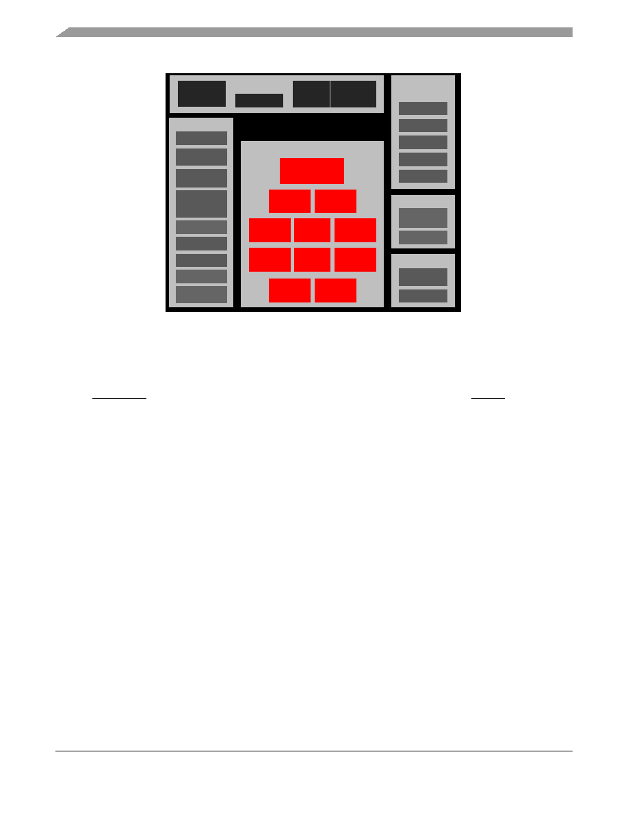
The new MC9328MX1 features the advanced and power-
efficient ARM920TTM core that operates at speeds up to
200 MHz. Integrated modules, which include an LCD
controller, static RAM, USB support, an A/D converter (with
touch panel control), and an MMC/SD host controller,
support a suite of peripherals to enhance any product seeking
to provide a rich multimedia experience. In addition, the
MC9328MX1 is the first BluetoothTM technology-ready
applications processor. It is packaged in a 256-pin Mold
Array Process-Ball Grid Array (MAPBGA). Figure 1 on
page 2 shows the functional block diagram of the
MC9328MX1.
MC9328MX1/D
Rev. 3.0, 12/2003
MC9328MX1
(i.MX1) Integrated
Portable System
Processor
Contents
1 Introduction . . . . . . . . . . . . . . . . . . . . . . . . . . . . . . . 1
2 Signals and Connections . . . . . . . . . . . . . . . . . . . . 6
3 Specifications . . . . . . . . . . . . . . . . . . . . . . . . . . . . 14
4 Pin-Out and Package Information . . . . . . . . . . . . 93
Contact Information . . . . . . . . . . . . . . . . . . . Last Page
MC9328MX1
MC9328MX1 Advance Information, Rev. 4
2
Freescale Semiconductor
Introduction
Figure 1. MC9328MX1 Functional Block Diagram
1.1 Conventions
This document uses the following conventions:
∑
OVERBAR is used to indicate a signal that is active when pulled low: for example, RESET.
∑
Logic level one is a voltage that corresponds to Boolean true (1) state.
∑
Logic level zero is a voltage that corresponds to Boolean false (0) state.
∑
To set a bit or bits means to establish logic level one.
∑
To clear a bit or bits means to establish logic level zero.
∑
A signal is an electronic construct whose state conveys or changes in state convey information.
∑
A pin is an external physical connection. The same pin can be used to connect a number of signals.
∑
Asserted means that a discrete signal is in active logic state.
-- Active low signals change from logic level one to logic level zero.
-- Active high signals change from logic level zero to logic level one.
∑
Negated means that an asserted discrete signal changes logic state.
-- Active low signals change from logic level zero to logic level one.
-- Active high signals change from logic level one to logic level zero.
∑
LSB means least significant bit or bits, and MSB means most significant bit or bits. References to low and
high bytes or words are spelled out.
∑
Numbers preceded by a percent sign (%) are binary. Numbers preceded by a dollar sign ($) or 0x are
hexadecimal.
Watchdog
GPIO
LCD Controller
JTAG/ICE
CGM
Timer 1 & 2
PWM
Standard
Bootstrap
Connectivity
System Control
I2C
MMC/SD
SPI 1 and
UART 1
UART 2 & 3
USB Device
SmartCard I/F
Bluetooth
Memory StickÆ
SSI/I2S 1 & 2
Analog Signal
Human Interface
Video Port
Multimedia
Multimedia
Power
RTC
Bus
DMAC
Interrupt
VMMU
CPU Complex
I Cache
AIPI 1
AIPI 2
D Cache
eSRAM
EIM &
ARM9TDMITM
System I/O
Control
(DPLLx2)
Controller
Control
(11 Chnl)
(128K)
SDRAMC
Accelerator
Accelerator
Processor
SPI 2
Host Controller
MC9328MX1

Introduction
MC9328MX1 Advance Information, Rev. 4
Freescale Semiconductor
3
1.2 Features
To support a wide variety of applications, the MC9328MX1 provides a robust array of features, including the
following:
∑
ARM920T Microprocessor Core
∑
AHB to IP Bus Interfaces (AIPIs)
∑
External Interface Module (EIM)
∑
SDRAM Controller (SDRAMC)
∑
DPLL Clock and Power Control Module
∑
Three Universal Asynchronous Receiver/Transmitters (UART 1 UART 2 and UART 3)
∑
Two Serial Peripheral Interfaces (SPI)
∑
Two General-Purpose 32-bit Counters/Timers
∑
Watchdog Timer
∑
Real-Time Clock/Sampling Timer (RTC)
∑
LCD Controller (LCDC)
∑
Pulse-Width Modulation (PWM) Module
∑
Universal Serial Bus (USB) Device
∑
Multimedia Card and Secure Digital (MMC/SD) Host Controller Module
∑
Memory StickÆ Host Controller (MSHC)
∑
SmartCard Interface Module (SIM)
∑
Direct Memory Access Controller (DMAC)
∑
Two Synchronous Serial Interfaces and Inter-IC Sound (SSI 1 and SSI 2/I
2
S) Module
∑
Inter-IC (I
2
C) Bus Module
∑
Video Port
∑
General-Purpose I/O (GPIO) Ports
∑
Bootstrap Mode
∑
Analog Signal Processing (ASP) Module
∑
Bluetooth Accelerator (BTA)
∑
Multimedia Accelerator (MMA)
∑
256-pin MAPBGA Package
1.3 Target Applications
The MC9328MX1 is targeted for advanced information appliances, smart phones, Web browsers, digital MP3
audio players, handheld computers based on the popular Palm OS platform, and messaging applications such as
Motorola's wireless cellular products, including the Accompli
TM
008 GSM/GPRS interactive communicator.

MC9328MX1 Advance Information, Rev. 4
4
Freescale Semiconductor
Introduction
1.4 Document Revision History
The following table provides revision history for this release. This history includes technical content revisions only
and not stylistic or grammatical changes.
1.5 Product Documentation
The following documents are required for a complete description of the MC9328MX1 and are necessary to design
properly with the device. Especially for those not familiar with the ARM920T processor or previous DragonBall
products, the following documents are helpful when used in conjunction with this manual.
ARM Architecture Reference Manual (ARM Ltd., order number ARM DDI 0100)
ARM9DT1 Data Sheet Manual (ARM Ltd., order number ARM DDI 0029)
ARM Technical Reference Manual (ARM Ltd., order number ARM DDI 0151C)
EMT9 Technical Reference Manual (ARM Ltd., order number DDI O157E)
MC9328MX1 Product Brief (order number MC9328MX1P/D)
MC9328MX1S Reference Manual (order number MC9328MX1SRM/D)
MC68VZ328 Product Brief (order number MC68VZ328P/D)
MC68VZ328 User's Manual (order number MC68VZ328UM/D)
MC68VZ328 User's Manual Addendum (order number MC68VZ328UMAD/D)
MC68SZ328 Product Brief (order number MC68SZ328P/D)
MC68SZ328 User's Manual (order number MC68SZ328UM/D)
The Motorola manuals are available on the Motorola Semiconductors Web site at http://www.motorola.com/
semiconductors. These documents may be downloaded directly from the Motorola Web site, or printed versions
may be ordered. The ARM Ltd. documentation is available from http://www.arm.com.
Table 1. MC9328MX1 Data Sheet Revision History
Revision Location
Revision
Throughout
Clarified instances where BCLK signal is burst clock.
Table 4 on page 14
Maximum Ratings table replaced.
Section 3.3, "Power Sequence
Requirements" on page 15
Added reference to AN2537.
Section 3.12, "Bluetooth Accelerator"
on page 58
Added "Important" note regarding no software support for the BTA.
Introduction
MC9328MX1 Advance Information, Rev. 4
Freescale Semiconductor
5
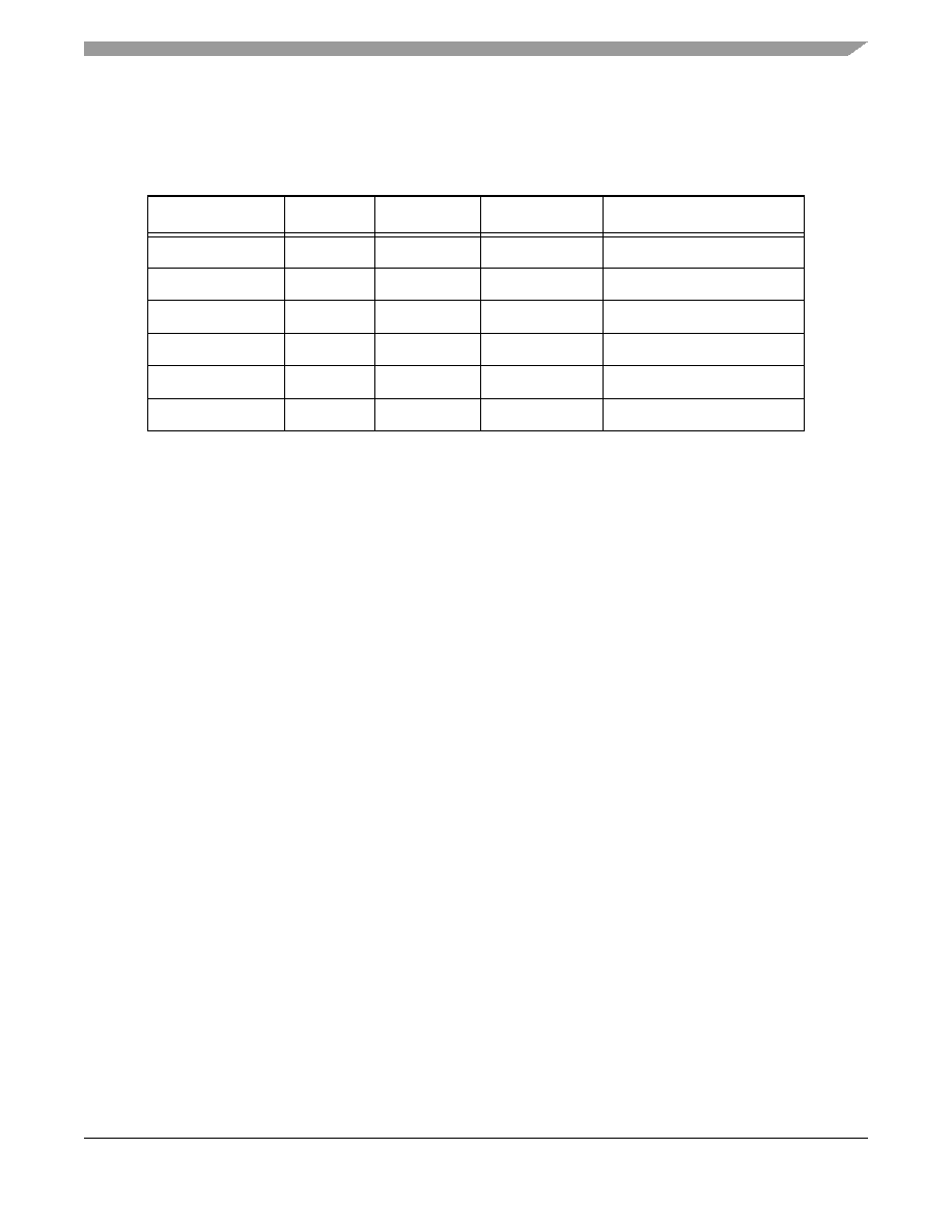
1.6 Ordering Information
Table 2 provides ordering information for the 256-lead mold array process ball grid array (MAPBGA) package.
Table 2. MC9328MX1 Ordering Information
Package Type
Frequency
Temperature
Solderball Type
Order Number
256-lead MAPBGA
200 MHz
0∞C to 70∞C
Standard
MC9328MX1VH20(R2)
256-lead MAPBGA
200 MHz
0∞C to 70∞C
Pb-free
MC9328MX1VM20(R2)
256-lead MAPBGA
200 MHz
-30∞C to 70∞C
Standard
MC9328MX1DVH20(R2)
256-lead MAPBGA
200 MHz
-30∞C to 70∞C
Pb-free
MC9328MX1DVM20(R2)
256-lead MAPBGA
150 MHz
-40∞C to 85∞C
Standard
MC9328MX1CVH15(R2)
256-lead MAPBGA
150 MHz
-40∞C to 85∞C
Pb-free
MC9328MX1CVM15(R2)