Motorola reserves the right to make changes without further notice to any products herein to improve reliability, function or
design. Motorola does not assume any liability arising out of the application or use of any product or circuit described herein;
neither does it convey any license under its patent rights nor the rights of others. Motorola products are not designed, intended,
or authorized for use as components in systems intended for surgical implant into the body, or other applications intended to
support or sustain life, or for any other application in which the failure of the Motorola product could create a situation where
personal injury or death may occur. Should Buyer purchase or use Motorola products for any such unintended or unauthorized
application, Buyer shall indemnify and hold Motorola and its officers, employees, subsidiaries, affiliates, and distributors harmless
against all claims, costs, damages, and expenses, and reasonable attorney fees arising out of, directly or indirectly, any claim of
personal injury or death associated with such unintended or unauthorized use, even if such claim alleges that Motorola was
negligent regarding the design or manufacture of the part.
DOCUMENT NUMBER
9S12DP256BDGV2/D
1
MC9S12DP256B
Device User Guide
V02.14
Covers also
MC9S12DT256C, MC9S12DJ256C,
MC9S12DG256C, MC9S12DT256B,
MC9S12DJ256B, MC9S12DG256B
MC9S12A256B
Original Release Date: 29 Mar 2001
Revised: Mar 5, 2003
Motorola, Inc
F
r
e
e
s
c
a
l
e
S
e
m
i
c
o
n
d
u
c
t
o
r
,
I
Freescale Semiconductor, Inc.
For More Information On This Product,
Go to: www.freescale.com
n
c
.
.
.
Motorola reserves the right to make changes without further notice to any products herein to improve reliability, function or
design. Motorola does not assume any liability arising out of the application or use of any product or circuit described herein;
neither does it convey any license under its patent rights nor the rights of others. Motorola products are not designed, intended,
or authorized for use as components in systems intended for surgical implant into the body, or other applications intended to
support or sustain life, or for any other application in which the failure of the Motorola product could create a situation where
personal injury or death may occur. Should Buyer purchase or use Motorola products for any such unintended or unauthorized
application, Buyer shall indemnify and hold Motorola and its officers, employees, subsidiaries, affiliates, and distributors harmless
against all claims, costs, damages, and expenses, and reasonable attorney fees arising out of, directly or indirectly, any claim of
personal injury or death associated with such unintended or unauthorized use, even if such claim alleges that Motorola was
negligent regarding the design or manufacture of the part.
DOCUMENT NUMBER
9S12DP256BDGV2/D
2
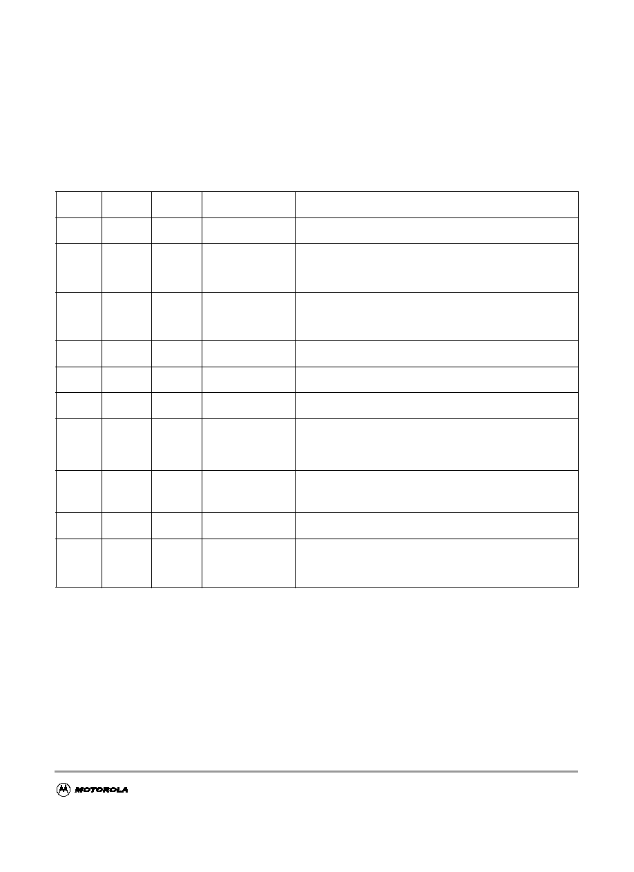
Revision History
Version
Number
Revision
Date
Effective
Date
Author
Description of Changes
V01.00
29 MAR
2001
29 MAR
2001
Initial version.
V01.01
8 MAY
2001
8 MAY
2001
VDD5 spec change 4.5V . . 5.25V
Current Injection on single pin +- 2.5mA
added DC bias level on EXTAL pin
minor cosmetics and corrected typos
V02.00
16 May
2001
16 May
2001
changed ATD Electrical Characteristics seperate coupling ratio for
positive and negative bulk current injection
added pinout for 80QFP
corrected SPI timing
V02.01
5 June
2001
corrected Expanded Bus Timing Characteristics
V02.02
14 June
2001
Some corrections on pin usage after review
V02.03
18 June
2001
Minor corrections with respect to format and wording
Added SRAM data retention disclaimer
V02.04
26 June
2001
Changed Oscillator Characteristics t
CQOUT
max 2.5s and replaced
Clock Monitor Time-out by Clock Monitor Failure Assert Frequency
Changed Self Clock Mode Frequency min 1MHz and max 5.5MHz
Changed I
DDPS
(RTI and COP disabled) to 400uA
V02.05
11 July
2001
Corrected f
ref
and REFDV/SYNR Settings for PLL Stabilization
Delay Measurements, added t
EXTR
and t
EXTF
to Oscillator
Characteristics, Corrected t
EXTL
and t
EXTH
values
V02.06
17 July
2001
Added thermal resistance for LQFP 80, added PCB layout proposal
for power and ground connections
V02.07
24 July
2001
Added Document Names
Variable definitions and Names have been hidden
Added Maskset 1K79X
Modified description in chapter A.5.2 Oscillator
F
r
e
e
s
c
a
l
e
S
e
m
i
c
o
n
d
u
c
t
o
r
,
I
Freescale Semiconductor, Inc.
For More Information On This Product,
Go to: www.freescale.com
n
c
.
.
.
MC9S12DP256B Device User Guide -- 9S12DP256BDGV2/D V02.14
3
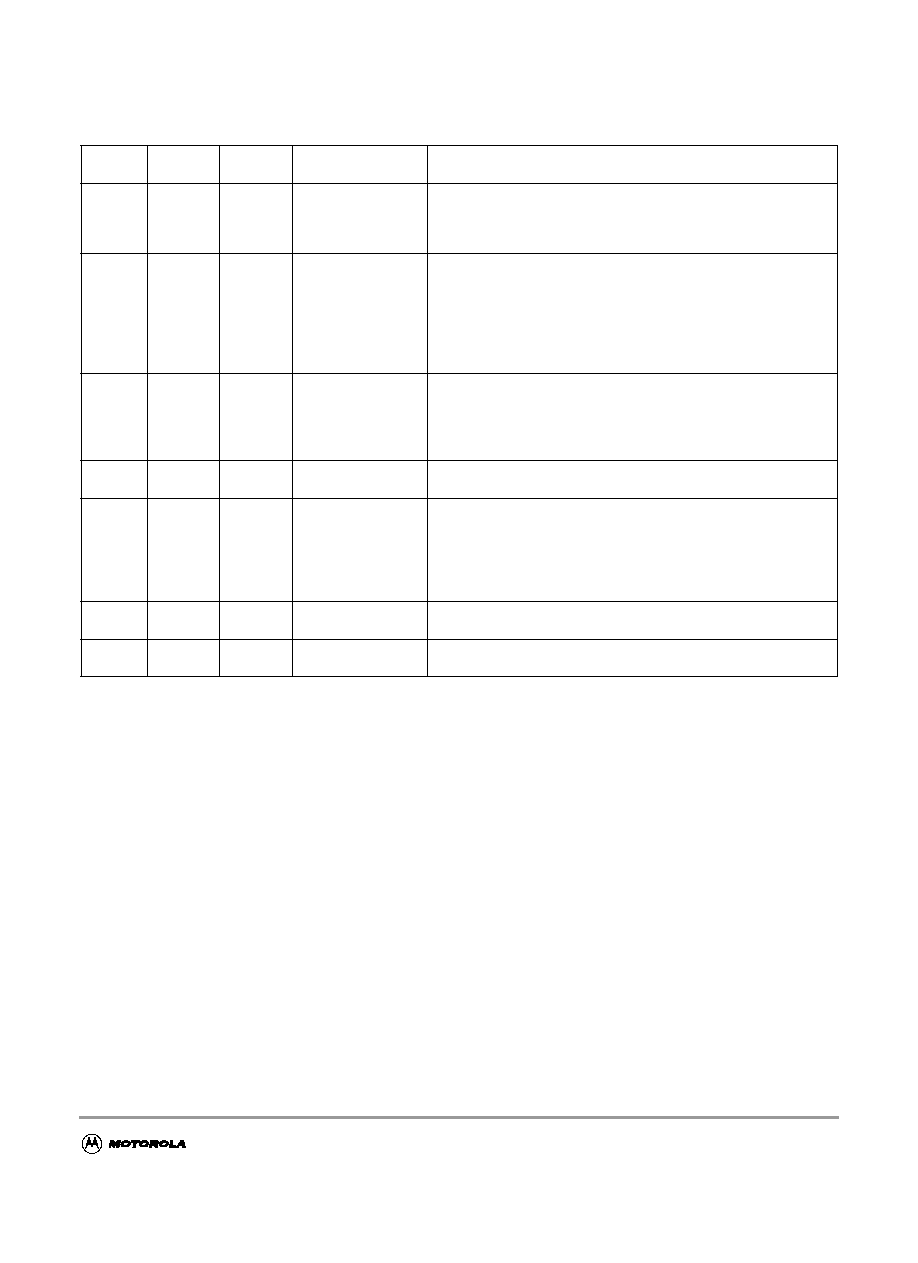
V02.08
24 August
2001
Corrected local enable bits in interrupt vector table
Corrected #33 - #36 in table A-20
A.4 Voltage Regulator characteristics was removed
A.1 to A.7 major rework according to feedback from PE
V02.09
12 Nov
2001
Changed document name and title to MC9..
Added table containing other devices covered by this document
Added NVM Blank check specificaiton
Added external ADC trigger to pin description
Updated A-7 Supply Current Characteristics
Updated Table0-1 Derivative Differences
Added Item8 to Table A-8
V02.10
28 Feb
2002
IOL/IOH reduced to 10mA/2mA for full/reduced drive
Changed ATD characteristic Cins max to 22pF
Changed VDD min VDDPLL min to 2.35V
Removed Oscillator startup time from POR or STOP
changed input capacitance for standard i/o pin to 6pF
V02.11
26 Mar
2002
Corrected NVM reliability spec
V02.12
12Aug
2002
added derivative differences for part number MC9S12D256C
added partID and maskset number for MC9S12D256D
added table with fixed defects on 2K79X
added table for HCS12 core configuration
Added detailed register map
Added pull device description to signal table
V02.13
25Sep
2002
corrected tables 0-1 and 0-2 Derivative Differences
added 80QFP DG256 pin assignment diagram
V02.14
28Feb
2003
added A256B parts to table 0-1 Derivative Differences
Version
Number
Revision
Date
Effective
Date
Author
Description of Changes
F
r
e
e
s
c
a
l
e
S
e
m
i
c
o
n
d
u
c
t
o
r
,
I
Freescale Semiconductor, Inc.
For More Information On This Product,
Go to: www.freescale.com
n
c
.
.
.

MC9S12DP256B Device User Guide -- V02.14
5
Table of Contents
Section 1 Introduction
1.1
Overview. . . . . . . . . . . . . . . . . . . . . . . . . . . . . . . . . . . . . . . . . . . . . . . . . . . . . . . . . . . . .17
1.2
Features . . . . . . . . . . . . . . . . . . . . . . . . . . . . . . . . . . . . . . . . . . . . . . . . . . . . . . . . . . . . .17
1.3
Modes of Operation . . . . . . . . . . . . . . . . . . . . . . . . . . . . . . . . . . . . . . . . . . . . . . . . . . . .19
1.4
Block Diagram . . . . . . . . . . . . . . . . . . . . . . . . . . . . . . . . . . . . . . . . . . . . . . . . . . . . . . . .20
1.5
Device Memory Map. . . . . . . . . . . . . . . . . . . . . . . . . . . . . . . . . . . . . . . . . . . . . . . . . . . .22
1.6
Detailed Register Map . . . . . . . . . . . . . . . . . . . . . . . . . . . . . . . . . . . . . . . . . . . . . . . . . .25
1.7
Part ID Assignments. . . . . . . . . . . . . . . . . . . . . . . . . . . . . . . . . . . . . . . . . . . . . . . . . . . .51
Section 2 Signal Description
2.1
Device Pinout . . . . . . . . . . . . . . . . . . . . . . . . . . . . . . . . . . . . . . . . . . . . . . . . . . . . . . . . .53
2.2
Signal Properties Summary . . . . . . . . . . . . . . . . . . . . . . . . . . . . . . . . . . . . . . . . . . . . . .56
2.3
Detailed Signal Descriptions. . . . . . . . . . . . . . . . . . . . . . . . . . . . . . . . . . . . . . . . . . . . . .59
2.3.1
EXTAL, XTAL -- Oscillator Pins . . . . . . . . . . . . . . . . . . . . . . . . . . . . . . . . . . . . . . . .59
2.3.2
RESET -- External Reset Pin . . . . . . . . . . . . . . . . . . . . . . . . . . . . . . . . . . . . . . . . . .60
2.3.3
TEST -- Test Pin . . . . . . . . . . . . . . . . . . . . . . . . . . . . . . . . . . . . . . . . . . . . . . . . . . . .60
2.3.4
VREGEN -- Voltage Regulator Enable Pin . . . . . . . . . . . . . . . . . . . . . . . . . . . . . . . .60
2.3.5
XFC -- PLL Loop Filter Pin . . . . . . . . . . . . . . . . . . . . . . . . . . . . . . . . . . . . . . . . . . . .60
2.3.6
BKGD / TAGHI / MODC -- Background Debug, Tag High, and Mode Pin . . . . . . . .60
2.3.7
PAD15 / AN15 / ETRIG1 -- Port AD Input Pin of ATD1 . . . . . . . . . . . . . . . . . . . . . .60
2.3.8
PAD[14:08] / AN[14:08] -- Port AD Input Pins of ATD1 . . . . . . . . . . . . . . . . . . . . . .61
2.3.9
PAD7 / AN07 / ETRIG0 -- Port AD Input Pin of ATD0 . . . . . . . . . . . . . . . . . . . . . . .61
2.3.10
PAD[06:00] / AN[06:00] -- Port AD Input Pins of ATD0 . . . . . . . . . . . . . . . . . . . . . .61
2.3.11
PA[7:0] / ADDR[15:8] / DATA[15:8] -- Port A I/O Pins . . . . . . . . . . . . . . . . . . . . . . .61
2.3.12
PB[7:0] / ADDR[7:0] / DATA[7:0] -- Port B I/O Pins . . . . . . . . . . . . . . . . . . . . . . . . .61
2.3.13
PE7 / NOACC / XCLKS -- Port E I/O Pin 7 . . . . . . . . . . . . . . . . . . . . . . . . . . . . . . . .61
2.3.14
PE6 / MODB / IPIPE1 -- Port E I/O Pin 6 . . . . . . . . . . . . . . . . . . . . . . . . . . . . . . . . .61
2.3.15
PE5 / MODA / IPIPE0 -- Port E I/O Pin 5 . . . . . . . . . . . . . . . . . . . . . . . . . . . . . . . . .62
2.3.16
PE4 / ECLK -- Port E I/O Pin 4 . . . . . . . . . . . . . . . . . . . . . . . . . . . . . . . . . . . . . . . . .62
2.3.17
PE3 / LSTRB / TAGLO -- Port E I/O Pin 3 . . . . . . . . . . . . . . . . . . . . . . . . . . . . . . . .62
2.3.18
PE2 / R/W -- Port E I/O Pin 2 . . . . . . . . . . . . . . . . . . . . . . . . . . . . . . . . . . . . . . . . . .62
2.3.19
PE1 / IRQ -- Port E Input Pin 1 . . . . . . . . . . . . . . . . . . . . . . . . . . . . . . . . . . . . . . . . .62
2.3.20
PE0 / XIRQ -- Port E Input Pin 0. . . . . . . . . . . . . . . . . . . . . . . . . . . . . . . . . . . . . . . .62
F
r
e
e
s
c
a
l
e
S
e
m
i
c
o
n
d
u
c
t
o
r
,
I
Freescale Semiconductor, Inc.
For More Information On This Product,
Go to: www.freescale.com
n
c
.
.
.