
MC9S12UF32
System on a Chip Guide
V01.05
Original Release Date: 17 JAN 2002
Revised: 03 Dec 2004
TSPG - 8/16 Bit MCU Design, HKG
Freescale Semiconductor, Inc.
This product has been designed for use in "Commercial" applications. Please see a description below.
Freescale's semiconductor products are classified into the following three tiers "Commercial", "Industrial", and "Automotive". A
product should only be used in applications appropriate to its tier. The recommended applications for products in the different
tiers are indicated below. For questions, please contact a Freescale sales representative.
Commercial: Typically 5 year applications - personal computers, PDA's, portable telecom products, consumer electronics, etc.
Industrial: Typically 10 year applications - installed telecom equipment, work stations, servers, etc. These products can also
be used for Commercial applications.
Automotive: Qualified per automotive industry standard methods.

2
Freescale Semiconductor
Freescale Semiconductor reserves the right to make changes without further notice to any products herein to improve reliability,
function or design. Freescale Semiconductor does not assume any liability arising out of the application or use of any product or
circuit described herein; neither does it convey any license under its patent rights nor the rights of others. Freescale
Semiconductor products are not designed, intended, or authorized for use as components in systems intended for surgical implant
into the body, or other applications intended to support or sustain life, or for any other application in which the failure of the
Freescale Semiconductor product could create a situation where personal injury or death may occur. Should Buyer purchase or
use Freescale Semiconductor products for any such unintended or unauthorized application, Buyer shall indemnify and hold
Freescale Semiconductor and its officers, employees, subsidiaries, affiliates, and distributors harmless against all claims, costs,
damages, and expenses, and reasonable attorney fees arising out of, directly or indirectly, any claim of personal injury or death
associated with such unintended or unauthorized use, even if such claim alleges that Freescale Semiconductor was negligent
regarding the design or manufacture of the part. Freescale
TM
and the Freescale logo are registered trademarks of Freescale
Semiconductor, Inc. Freescale Semiconductor, Inc. is an Equal Opportunity/Affirmative Action Employer.
© Freescale Semiconductor, Inc. 2004
Revision History
Release
Number
Date
Author
Summary of Changes
00.01
17JAN02
Y.H. Cheng
Initial Version
00.02
19FEB02
Y.H. Cheng
Modified SMRAM mapping to allow 1k byte 16-bit block mappable
to Vector Space. Update spec with review feedback.
00.03
26APR02
Y.H. Cheng
Modified Device pinout to separate D+ D- for high speed and low
speed operation. Remap Timer pins to Port R. Update BG
references.
00.04
16SEP02
Y.H. Cheng
Modified Device pinout per IP requirement
Add SCI
Update Interrupt information.
00.05
25SEP02
Y.H. Cheng
Change pin location for REF3V and VREGEN
minor update on module name references
remove references to pseudo stop and clock monitor
00.06
03JUN03
Y.H. Cheng
- Updated info for SMRAM3P5K2E in device memory map
- Updated EXTAL and XTAL supply rail information.
- Relocate SCI module base address from $70 to $C8
- Relocate ATA5HC module base address from $240 to $1C0
- Relocate PIM module base address from $80 to $240
- Relocate Interrupt Vectors
- Updated Phy evaluation pinout.
- Updated CFA00, CFA01 and CFA02 pin name to CFA0, CFA1 and
CFA2 respectively.
- Removed ESD and Latchup section in Electrical.
- Update Block Guide References
- Miscellaneous Typo mistakes.
00.07
11JUN03
Y.H. Cheng
- Update typo in interrupt vector table for Vector $C2
- Update typo in pin order of IOC[7:4] in signal properties table
- Specify run and wait IDDs in Electrical Section
- Specify stop IDD at room temperature in Electrical Section
00.08
13JUL03
Y.H. Cheng
- Change specification to include 64 pin option
- ROMCTL pin assigned to PJ2

3
Freescale Semiconductor
System on a Chip Guide -- 9S12UF32DGV1/D V01.05
01.00
21AUG03
Y.H. Cheng
- Removed all references to XCLKS, since function is removed.
- typo - replaced PRU with RPU.
- typo - replaced ATAHC with ATA5HC
- Removed references to clock monitor, since function is not
available.
- Update
JA
for 100-pin and 64-pin packages.
- Add footnotes on IRQ pin removal in 64-pin package
- Update Flash memory map out of reset.
- Add information on INITRM, INITRG, INITEE setting for example
application memory map
- Update clock distribution diagram to make it more intelligible
- Change table 2-3, 2-5 description using general purpose port
references instead of Functional module references.
- Stop IDD spec for -40C and 85C are removed
- Add other conditions for RUN Idd and Wait Idd.
01.01
28NOV03
Wai-On Law
- Minor typo corrections.
- Corrected `Background Debug Module' to `HCS12 Breakpoint' at
address $0028-$002F in table 1-1.
- Added detailed register map.
- Corrected the MSHC enable control in table 5-1.
- Added part ID $6311 for mask 1L47S.
01.02
23MAR04
Y.H. Cheng
- Removed all references and description on USB Physical
Endpoint 6
- Updated IDD, 3V and 5V I/O electricals and package thermal
resistance information
- Include Commercial tier note
- Update and add note to detailed register map.
01.03
20APR04
Wai-On Law
- Added PIM reference.
01.04
10MAY04
Wai-On Law
- Added package information as appendix B.
01.05
03DEC04
Wai-On Law
- Improved fig 1-1.
- Fixed consistency of 3.0v and 3.3v for VDD3X.
- Updated power dissipation formula.
- Added schematic and PCB layout recommendations.
- Added NVM, VREGU, CRGU electricals to appendix A.
Release
Number
Date
Author
Summary of Changes

System on a Chip Guide -- 9S12UF32DGV1/D V01.05
4
Freescale Semiconductor

5
Freescale Semiconductor
System on a Chip Guide -- 9S12UF32DGV1/D V01.05
Table of Contents
Section 1 Introduction
1.1
Overview. . . . . . . . . . . . . . . . . . . . . . . . . . . . . . . . . . . . . . . . . . . . . . . . . . . . . . . . . . . . .19
1.2
Features . . . . . . . . . . . . . . . . . . . . . . . . . . . . . . . . . . . . . . . . . . . . . . . . . . . . . . . . . . . . .19
1.3
Modes of Operation . . . . . . . . . . . . . . . . . . . . . . . . . . . . . . . . . . . . . . . . . . . . . . . . . . . .22
1.4
Block Diagram . . . . . . . . . . . . . . . . . . . . . . . . . . . . . . . . . . . . . . . . . . . . . . . . . . . . . . . .23
1.5
Device Memory Map. . . . . . . . . . . . . . . . . . . . . . . . . . . . . . . . . . . . . . . . . . . . . . . . . . . .24
1.5.1
Detailed Register Map . . . . . . . . . . . . . . . . . . . . . . . . . . . . . . . . . . . . . . . . . . . . . . . .26
1.6
Part ID Assignments. . . . . . . . . . . . . . . . . . . . . . . . . . . . . . . . . . . . . . . . . . . . . . . . . . . .46
Section 2 Signal Description
2.1
Device Pinout . . . . . . . . . . . . . . . . . . . . . . . . . . . . . . . . . . . . . . . . . . . . . . . . . . . . . . . . .49
2.2
Signal Properties Summary for 100-pin Package. . . . . . . . . . . . . . . . . . . . . . . . . . . . . .51
2.3
Signal Properties Summary for 64-pin Package. . . . . . . . . . . . . . . . . . . . . . . . . . . . . . .54
2.4
Detailed Signal Descriptions for 100-pin package . . . . . . . . . . . . . . . . . . . . . . . . . . . . .57
2.4.1
EXTAL, XTAL -- Oscillator Pins . . . . . . . . . . . . . . . . . . . . . . . . . . . . . . . . . . . . . . . .57
2.4.2
RESET -- External Reset Pin . . . . . . . . . . . . . . . . . . . . . . . . . . . . . . . . . . . . . . . . . .57
2.4.3
TEST -- Test Pin . . . . . . . . . . . . . . . . . . . . . . . . . . . . . . . . . . . . . . . . . . . . . . . . . . . .57
2.4.4
VREGEN -- Voltage Regulator Enable Pin . . . . . . . . . . . . . . . . . . . . . . . . . . . . . . . .57
2.4.5
BKGD / TAGHI / MODC -- Background Debug, Tag High & Mode Pin . . . . . . . . . .57
2.4.6
RPU -- USB D+ pull up resistor termination . . . . . . . . . . . . . . . . . . . . . . . . . . . . . . .57
2.4.7
RREF -- External bias resistor . . . . . . . . . . . . . . . . . . . . . . . . . . . . . . . . . . . . . . . . .57
2.4.8
DPF - USB Full Speed D+ data line . . . . . . . . . . . . . . . . . . . . . . . . . . . . . . . . . . . . . .58
2.4.9
DPH - USB High Speed D+ data line . . . . . . . . . . . . . . . . . . . . . . . . . . . . . . . . . . . . .58
2.4.10
DMF - USB Full Speed D- data line . . . . . . . . . . . . . . . . . . . . . . . . . . . . . . . . . . . . . .58
2.4.11
DMH - USB High Speed D- data line . . . . . . . . . . . . . . . . . . . . . . . . . . . . . . . . . . . . .58
2.4.12
PWROFF5V - power off 5V supply . . . . . . . . . . . . . . . . . . . . . . . . . . . . . . . . . . . . . .58
2.4.13
PWROFF3V - power off 3V supply . . . . . . . . . . . . . . . . . . . . . . . . . . . . . . . . . . . . . .58
2.4.14
REF3V - 3.3V reference for external regulator. . . . . . . . . . . . . . . . . . . . . . . . . . . . . .58
2.4.15
PA[7:0] / ADDR[15:8] / DATA[15:8] / CFD[15:8] / ATAD[15:8] -- Port A I/O Pins . . .58
2.4.16
PB[7:0] / ADDR[7:0] / DATA[7:0] / CFD[7:0] / ATAD[7:0] -- Port B I/O Pins . . . . . . .59
2.4.17
PE7 / NOACC -- Port E I/O Pin 7 . . . . . . . . . . . . . . . . . . . . . . . . . . . . . . . . . . . . . . .59
2.4.18
PE6 / MODB / IPIPE1 -- Port E I/O Pin 6 . . . . . . . . . . . . . . . . . . . . . . . . . . . . . . . . .59
2.4.19
PE5 / MODA / IPIPE0 -- Port E I/O Pin 5 . . . . . . . . . . . . . . . . . . . . . . . . . . . . . . . . .59

System on a Chip Guide -- 9S12UF32DGV1/D V01.05
6
Freescale Semiconductor
2.4.20
PE4 / ECLK-- Port E I/O Pin 4 / E-Clock Output . . . . . . . . . . . . . . . . . . . . . . . . . . . .59
2.4.21
PE3 / LSTRB / TAGLO -- Port E I/O Pin 3 / Low-Byte Strobe (LSTRB) . . . . . . . . . .60
2.4.22
PE2 / R/W -- Port E I/O Pin 2 / Read/Write. . . . . . . . . . . . . . . . . . . . . . . . . . . . . . . .60
2.4.23
PE1 / IRQ -- Port E input Pin 1 / Maskable Interrupt Pin . . . . . . . . . . . . . . . . . . . . .60
2.4.24
PE0 / XIRQ -- Port E input Pin 0 / Non Maskable Interrupt Pin . . . . . . . . . . . . . . . .60
2.4.25
PJ2 / MSSCLK/ROMCTL - Port J I/O Pin 2 . . . . . . . . . . . . . . . . . . . . . . . . . . . . . . . .60
2.4.26
PJ1 / MSSDIO - Port J I/O Pin 1 . . . . . . . . . . . . . . . . . . . . . . . . . . . . . . . . . . . . . . . .61
2.4.27
PJ0 / MSBS - Port J I/O Pin 0 . . . . . . . . . . . . . . . . . . . . . . . . . . . . . . . . . . . . . . . . . .61
2.4.28
PM[5:2] / SDDATA[3:0] - Port M I/O Pin [5:2] . . . . . . . . . . . . . . . . . . . . . . . . . . . . . .61
2.4.29
PM1 / SDCLK -- Port M I/O Pin 1 . . . . . . . . . . . . . . . . . . . . . . . . . . . . . . . . . . . . . . .61
2.4.30
PM0 / SDCMD -- Port M I/O Pin 0 . . . . . . . . . . . . . . . . . . . . . . . . . . . . . . . . . . . . . .61
2.4.31
PP7 / SRE / ACFD15 / AATAD15-- Port P I/O Pin 7. . . . . . . . . . . . . . . . . . . . . . . . .61
2.4.32
PP6 / SWE / ACFD14 / AATAD14-- Port P I/O Pin 6 . . . . . . . . . . . . . . . . . . . . . . . .62
2.4.33
PP5 / SALE / ACFD13 / AATAD13-- Port P I/O Pin 5. . . . . . . . . . . . . . . . . . . . . . . .62
2.4.34
PP4 / SCLE / ACFD12 / AATAD12-- Port P I/O Pin 4. . . . . . . . . . . . . . . . . . . . . . . .62
2.4.35
PP3 / SWP / ACFD11 / AATAD11-- Port P I/O Pin 3 . . . . . . . . . . . . . . . . . . . . . . . .62
2.4.36
PP2 / SCE / ACFD10 / AATAD10-- Port P I/O Pin 2. . . . . . . . . . . . . . . . . . . . . . . . .62
2.4.37
PP1 / SCD / ACFD9 / AATAD9-- Port P I/O Pin 1 . . . . . . . . . . . . . . . . . . . . . . . . . .63
2.4.38
PP0 / SBSY / ACFD8 / AATAD8-- Port P I/O Pin 0 . . . . . . . . . . . . . . . . . . . . . . . . .63
2.4.39
PQ[7:0] / SDAT[7:0] / ACFD[7:0] / AATAD[7:0]-- Port Q I/O Pins [7:0] . . . . . . . . . . .63
2.4.40
PR[1:0] / CFA[4:3] -- Port R I/O Pins [1:0] . . . . . . . . . . . . . . . . . . . . . . . . . . . . . . . .63
2.4.41
PR[2] / CFA[5] / RXD -- Port R I/O Pins [2]. . . . . . . . . . . . . . . . . . . . . . . . . . . . . . . .63
2.4.42
PR[3] / CFA[6] / TXD -- Port R I/O Pins [3] . . . . . . . . . . . . . . . . . . . . . . . . . . . . . . . .64
2.4.43
PR[7:4] / CFA[10:7] / IOC[7:4] -- Port R I/O Pins [7:4] . . . . . . . . . . . . . . . . . . . . . . .64
2.4.44
PS7 / CFRDY(CFIREQ) / ATAINTQ -- Port S I/O Pin 7 . . . . . . . . . . . . . . . . . . . . . .64
2.4.45
PS6 / CFWE / ATADMARQ -- Port S I/O Pin 6 . . . . . . . . . . . . . . . . . . . . . . . . . . . . .64
2.4.46
PS5 / CFIOWR / ATAIOWR -- Port S I/O Pin 5 . . . . . . . . . . . . . . . . . . . . . . . . . . . .64
2.4.47
PS4 / CFIORD / ATAIORD -- Port S I/O Pin 4 . . . . . . . . . . . . . . . . . . . . . . . . . . . . .65
2.4.48
PS3 / CFCE2 / ATACS1 -- Port S I/O Pin 3 . . . . . . . . . . . . . . . . . . . . . . . . . . . . . . .65
2.4.49
PS2 / CFIOIS16 -- Port S I/O Pin 2. . . . . . . . . . . . . . . . . . . . . . . . . . . . . . . . . . . . . .65
2.4.50
PS1 / CFOE -- Port S I/O Pin 1. . . . . . . . . . . . . . . . . . . . . . . . . . . . . . . . . . . . . . . . .65
2.4.51
PS0 / CFCE1 / ATACS0 -- Port S I/O Pin 0 . . . . . . . . . . . . . . . . . . . . . . . . . . . . . . .65
2.4.52
PT[3:0] / IOC[3:0]-- Port T I/O Pins [3:0] . . . . . . . . . . . . . . . . . . . . . . . . . . . . . . . . . .66
2.4.53
PU[5:3] / CFA[2:0] / ATADA[2:0] -- Port U I/O Pins [5:3] . . . . . . . . . . . . . . . . . . . . .66
2.4.54
PU2 / CFREG -- Port U I/O Pin 2 . . . . . . . . . . . . . . . . . . . . . . . . . . . . . . . . . . . . . . .66
2.4.55
PU1 / CFINPACK / ATADMACK -- Port U I/O Pin 1 . . . . . . . . . . . . . . . . . . . . . . . . .66

7
Freescale Semiconductor
System on a Chip Guide -- 9S12UF32DGV1/D V01.05
2.4.56
PU0 / CFWAIT / ATAIORDY -- Port U I/O Pin 0 . . . . . . . . . . . . . . . . . . . . . . . . . . . .66
2.5
Detailed Signal Descriptions for 64-pin package . . . . . . . . . . . . . . . . . . . . . . . . . . . . . .67
2.5.1
EXTAL, XTAL -- Oscillator Pins . . . . . . . . . . . . . . . . . . . . . . . . . . . . . . . . . . . . . . . .67
2.5.2
RESET -- External Reset Pin . . . . . . . . . . . . . . . . . . . . . . . . . . . . . . . . . . . . . . . . . .67
2.5.3
TEST -- Test Pin . . . . . . . . . . . . . . . . . . . . . . . . . . . . . . . . . . . . . . . . . . . . . . . . . . . .67
2.5.4
BKGD / TAGHI / MODC -- Background Debug, Tag High & Mode Pin . . . . . . . . . .67
2.5.5
RPU -- USB D+ pull up resistor termination . . . . . . . . . . . . . . . . . . . . . . . . . . . . . . .67
2.5.6
RREF -- External bias resistor . . . . . . . . . . . . . . . . . . . . . . . . . . . . . . . . . . . . . . . . .67
2.5.7
DPF - USB Full Speed D+ data line . . . . . . . . . . . . . . . . . . . . . . . . . . . . . . . . . . . . . .67
2.5.8
DPH - USB High Speed D+ data line . . . . . . . . . . . . . . . . . . . . . . . . . . . . . . . . . . . . .68
2.5.9
DMF - USB Full Speed D- data line . . . . . . . . . . . . . . . . . . . . . . . . . . . . . . . . . . . . . .68
2.5.10
DMH - USB High Speed D- data line . . . . . . . . . . . . . . . . . . . . . . . . . . . . . . . . . . . . .68
2.5.11
REF3V - 3.3V reference for external regulator. . . . . . . . . . . . . . . . . . . . . . . . . . . . . .68
2.5.12
PA[5:0] / ADDR[13:8] / DATA[13:8] / CFD[13:8] / ATAD[13:8] -- Port A I/O Pins . . .68
2.5.13
PA[6] / ADDR[14] / DATA[14] / CFD[14] / ATAD[14] / MSBS-- Port A I/O Pins . . . .68
2.5.14
PA[7] / ADDR[15] / DATA[15] / CFD[15] / ATAD[15] -- Port A I/O Pins . . . . . . . . . .69
2.5.15
PB[7:0] / ADDR[7:0] / DATA[7:0]/ CFD[7:0] / ATAD[7:0] / IOC[7:0] -- Port B I/O Pins .
69
2.5.16
PE7 / NOACC / CAF10-- Port E I/O Pin 7. . . . . . . . . . . . . . . . . . . . . . . . . . . . . . . . .69
2.5.17
PE6 / MODB / IPIPE1 / CFA9 -- Port E I/O Pin 6 . . . . . . . . . . . . . . . . . . . . . . . . . . .69
2.5.18
PE5 / MODA / IPIPE0 / CFA8 -- Port E I/O Pin 5 . . . . . . . . . . . . . . . . . . . . . . . . . . .69
2.5.19
PE4 / ECLK-- Port E I/O Pin 4 / E-Clock Output . . . . . . . . . . . . . . . . . . . . . . . . . . . .69
2.5.20
PE3 / LSTRB / TAGLO / CFA3 -- Port E I/O Pin 3 / Low-Byte Strobe (LSTRB) . . . .70
2.5.21
PE2 / R/W -- Port E I/O Pin 2 / Read/Write. . . . . . . . . . . . . . . . . . . . . . . . . . . . . . . .70
2.5.22
PE0 / XIRQ -- Port E input Pin 0 / Non Maskable Interrupt Pin . . . . . . . . . . . . . . . .70
2.5.23
PJ2 / ATACS1 / SWP / CFCE2 / ROMCTL - Port J I/O Pin 2 . . . . . . . . . . . . . . . . . .70
2.5.24
PJ1 / ATACS0 / SCLE / CFCE1 - Port J I/O Pin 1 . . . . . . . . . . . . . . . . . . . . . . . . . . .71
2.5.25
PJ0 / ATAIOWR / SALE / CFIOWR - Port J I/O Pin 0 . . . . . . . . . . . . . . . . . . . . . . . .71
2.5.26
PM4 / IOC3 / SDDATA2 / SBSY / CFIOIS16 -- Port M I/O Pin 4 . . . . . . . . . . . . . . .71
2.5.27
PM3 / IOC2 / SDDATA1 / SCE / CFINPACK -- Port M I/O Pin 3 . . . . . . . . . . . . . . .71
2.5.28
PQ7 / SDAT7 / CFA7 / IOC7 -- Port Q I/O Pins 7 . . . . . . . . . . . . . . . . . . . . . . . . . . .71
2.5.29
PQ6 / SDAT6 / CFA6 / SDCLK / IOC6 -- Port Q I/O Pins 6 . . . . . . . . . . . . . . . . . . .72
2.5.30
PQ5 / SDAT5 / CFA5 / SDCMD / IOC5 -- Port Q I/O Pins 5 . . . . . . . . . . . . . . . . . . .72
2.5.31
PQ4 / SDAT4 / CFA4 / ATADMACK / IOC4 -- Port Q I/O Pins 4 . . . . . . . . . . . . . . .72
2.5.32
PQ3 / SDAT3 / CFIORD / ATAIORD -- Port Q I/O Pins 3 . . . . . . . . . . . . . . . . . . . . .72
2.5.33
PQ[2:0] / SDAT[2:0] / CFA[2:0] / ATADA[2:0]-- Port Q I/O Pins [2:0] . . . . . . . . . . . .72

System on a Chip Guide -- 9S12UF32DGV1/D V01.05
8
Freescale Semiconductor
2.5.34
PS7 / CFRDY(CFIREQ) / ATAINTQ / MSSDIO -- Port S I/O Pin 7. . . . . . . . . . . . . .73
2.5.35
PS6 / CFWE / ATADMARQ / MSCLK -- Port S I/O Pin 6 . . . . . . . . . . . . . . . . . . . . .73
2.5.36
PS5 / TXD -- Port S I/O Pin 5 . . . . . . . . . . . . . . . . . . . . . . . . . . . . . . . . . . . . . . . . . .73
2.5.37
PS4 / RXD -- Port S I/O Pin 4 . . . . . . . . . . . . . . . . . . . . . . . . . . . . . . . . . . . . . . . . . .73
2.5.38
PT1 / IOC1 / SDDATA3 / SWE / CFOE -- Port T I/O Pin 1 . . . . . . . . . . . . . . . . . . . .73
2.5.39
PT0 / IOC0 / SDDATA0 / SRE / CFREG -- Port T I/O Pin 0 . . . . . . . . . . . . . . . . . . .73
2.5.40
PU0 / CFWAIT / ATAIORDY / SCD -- Port U I/O Pin 0. . . . . . . . . . . . . . . . . . . . . . .74
2.6
Power Supply Pins . . . . . . . . . . . . . . . . . . . . . . . . . . . . . . . . . . . . . . . . . . . . . . . . . . . . .74
2.6.1
VDDR, VSSR - Power & Ground Pins for I/O Drivers & for Internal Voltage Regulator.
74
2.6.2
VDD - Core Power Pin . . . . . . . . . . . . . . . . . . . . . . . . . . . . . . . . . . . . . . . . . . . . . . . .75
2.6.3
VDDX, VSSX - Power & Ground Pins for I/O Drivers . . . . . . . . . . . . . . . . . . . . . . . .75
2.6.4
VDD3X, VSS3X - Power & Ground Pins for I/O Drivers . . . . . . . . . . . . . . . . . . . . . .75
2.6.5
VDDA, VSSA, VSSA1 - USB PHY Power Pins . . . . . . . . . . . . . . . . . . . . . . . . . . . . .75
Section 3 System Clock Description
Section 4 Modes of Operation
4.1
Overview. . . . . . . . . . . . . . . . . . . . . . . . . . . . . . . . . . . . . . . . . . . . . . . . . . . . . . . . . . . . .78
4.2
Modes of Operation . . . . . . . . . . . . . . . . . . . . . . . . . . . . . . . . . . . . . . . . . . . . . . . . . . . .78
4.2.1
Normal Operating Modes . . . . . . . . . . . . . . . . . . . . . . . . . . . . . . . . . . . . . . . . . . . . . .79
4.2.2
Special Operating Modes. . . . . . . . . . . . . . . . . . . . . . . . . . . . . . . . . . . . . . . . . . . . . .81
4.3
Internal Visibility . . . . . . . . . . . . . . . . . . . . . . . . . . . . . . . . . . . . . . . . . . . . . . . . . . . . . . .82
4.4
Security. . . . . . . . . . . . . . . . . . . . . . . . . . . . . . . . . . . . . . . . . . . . . . . . . . . . . . . . . . . . . .82
4.4.1
Securing the Microcontroller . . . . . . . . . . . . . . . . . . . . . . . . . . . . . . . . . . . . . . . . . . .83
4.4.2
Operation of the Secured Microcontroller . . . . . . . . . . . . . . . . . . . . . . . . . . . . . . . . .83
4.4.3
Unsecuring the Microcontroller . . . . . . . . . . . . . . . . . . . . . . . . . . . . . . . . . . . . . . . . .83
4.5
Low Power Modes . . . . . . . . . . . . . . . . . . . . . . . . . . . . . . . . . . . . . . . . . . . . . . . . . . . . .84
4.5.1
Stop . . . . . . . . . . . . . . . . . . . . . . . . . . . . . . . . . . . . . . . . . . . . . . . . . . . . . . . . . . . . . .84
4.5.2
Wait . . . . . . . . . . . . . . . . . . . . . . . . . . . . . . . . . . . . . . . . . . . . . . . . . . . . . . . . . . . . . .84
4.5.3
Run. . . . . . . . . . . . . . . . . . . . . . . . . . . . . . . . . . . . . . . . . . . . . . . . . . . . . . . . . . . . . . .84
Section 5 Resets and Interrupts
5.1
Overview. . . . . . . . . . . . . . . . . . . . . . . . . . . . . . . . . . . . . . . . . . . . . . . . . . . . . . . . . . . . .85
5.2
Vectors . . . . . . . . . . . . . . . . . . . . . . . . . . . . . . . . . . . . . . . . . . . . . . . . . . . . . . . . . . . . . .85
5.2.1
Vector Table. . . . . . . . . . . . . . . . . . . . . . . . . . . . . . . . . . . . . . . . . . . . . . . . . . . . . . . .85
5.3
Resets . . . . . . . . . . . . . . . . . . . . . . . . . . . . . . . . . . . . . . . . . . . . . . . . . . . . . . . . . . . . . .87

9
Freescale Semiconductor
System on a Chip Guide -- 9S12UF32DGV1/D V01.05
5.3.1
Reset Summary Table . . . . . . . . . . . . . . . . . . . . . . . . . . . . . . . . . . . . . . . . . . . . . . . .87
5.3.2
Effects of Reset . . . . . . . . . . . . . . . . . . . . . . . . . . . . . . . . . . . . . . . . . . . . . . . . . . . . .87
Section 6 HCS12 Core Block Description
6.1
CPU12 Block Description . . . . . . . . . . . . . . . . . . . . . . . . . . . . . . . . . . . . . . . . . . . . . . . .88
6.2
HCS12 Background Debug Module (BDM) Block Description . . . . . . . . . . . . . . . . . . . .88
6.3
HCS12 Breakpoint (BKP) Block Description . . . . . . . . . . . . . . . . . . . . . . . . . . . . . . . . .88
6.4
HCS12 Interrupt (INT) Block Description . . . . . . . . . . . . . . . . . . . . . . . . . . . . . . . . . . . .88
6.5
HCS12 Multiplexed External Bus Interface (MEBI) Block Description . . . . . . . . . . . . . .88
6.6
HCS12 Module Mapping Control (MMC) Block Description . . . . . . . . . . . . . . . . . . . . . .88
Section 7 ATA5 Host Controller (ATA5HC) Block Description
7.1
Device-specific information. . . . . . . . . . . . . . . . . . . . . . . . . . . . . . . . . . . . . . . . . . . . . . .89
Section 8 Compact Flash Host Controller (CFHC) Block Description
8.1
Device-specific information. . . . . . . . . . . . . . . . . . . . . . . . . . . . . . . . . . . . . . . . . . . . . . .89
Section 9 Clock Reset Generator (CRG_U) Block Description
9.1
Device-specific information. . . . . . . . . . . . . . . . . . . . . . . . . . . . . . . . . . . . . . . . . . . . . . .89
Section 10 Flash EEPROM 32K (FTS32K) Block Description
10.1
Device-specific information. . . . . . . . . . . . . . . . . . . . . . . . . . . . . . . . . . . . . . . . . . . . . . .90
Section 11 Integrated Queue Controller (IQUE) Block Description
11.1
Device-specific information. . . . . . . . . . . . . . . . . . . . . . . . . . . . . . . . . . . . . . . . . . . . . . .90
Section 12 Memorystick Host Controller (MSHC) Block Description
12.1
Device-specific information. . . . . . . . . . . . . . . . . . . . . . . . . . . . . . . . . . . . . . . . . . . . . . .91
Section 13 Oscillator (OSC) Block Description
13.1
Device-specific information. . . . . . . . . . . . . . . . . . . . . . . . . . . . . . . . . . . . . . . . . . . . . . .91
Section 14 Port Integration Module (PIM) Block Description
14.1
Device-specific information. . . . . . . . . . . . . . . . . . . . . . . . . . . . . . . . . . . . . . . . . . . . . . .92
Section 15 Serial Communication Interface (SCI) Block Description
15.1
Device-specific information. . . . . . . . . . . . . . . . . . . . . . . . . . . . . . . . . . . . . . . . . . . . . . .92

System on a Chip Guide -- 9S12UF32DGV1/D V01.05
10
Freescale Semiconductor
Section 16 Secured Digital Host Controller (SDHC) Block Description
16.1
Device-specific information. . . . . . . . . . . . . . . . . . . . . . . . . . . . . . . . . . . . . . . . . . . . . . .92
Section 17 Smartmedia Host Controller (SMHC) Block Description
17.1
Device-specific information. . . . . . . . . . . . . . . . . . . . . . . . . . . . . . . . . . . . . . . . . . . . . . .93
Section 18 Smartmedia RAM (SMRAM) Block Description
18.1
Device-specific information. . . . . . . . . . . . . . . . . . . . . . . . . . . . . . . . . . . . . . . . . . . . . . .93
Section 19 Timer (TIM) Block Description
19.1
Device-specific information. . . . . . . . . . . . . . . . . . . . . . . . . . . . . . . . . . . . . . . . . . . . . . .93
Section 20 USB2.0 Controller (USB20D6E2F) Block Description
20.1
Device-specific information. . . . . . . . . . . . . . . . . . . . . . . . . . . . . . . . . . . . . . . . . . . . . . .93
Section 21 Voltage Regulator (VREG_U) Block Description
21.1
Device-specific information. . . . . . . . . . . . . . . . . . . . . . . . . . . . . . . . . . . . . . . . . . . . . . .94
Section 22 Schematic and PCB Layout Design Recommendations
22.1
Schematic Design with the MC9S12UF32 and a USB interface . . . . . . . . . . . . . . . . . .94
22.1.1
Power Supply Notes. . . . . . . . . . . . . . . . . . . . . . . . . . . . . . . . . . . . . . . . . . . . . . . . . .95
22.1.2
Clocking Notes . . . . . . . . . . . . . . . . . . . . . . . . . . . . . . . . . . . . . . . . . . . . . . . . . . . . . .95
22.2
PCB Design Recommendation. . . . . . . . . . . . . . . . . . . . . . . . . . . . . . . . . . . . . . . . . . . .96
Appendix A Electrical Characteristics
A.1
General. . . . . . . . . . . . . . . . . . . . . . . . . . . . . . . . . . . . . . . . . . . . . . . . . . . . . . . . . . . . . .97
A.1.1
Parameter Classification . . . . . . . . . . . . . . . . . . . . . . . . . . . . . . . . . . . . . . . . . . . . . .97
A.1.2
Power Supply . . . . . . . . . . . . . . . . . . . . . . . . . . . . . . . . . . . . . . . . . . . . . . . . . . . . . . .97
A.1.3
Pins . . . . . . . . . . . . . . . . . . . . . . . . . . . . . . . . . . . . . . . . . . . . . . . . . . . . . . . . . . . . . .98
A.1.4
Current Injection. . . . . . . . . . . . . . . . . . . . . . . . . . . . . . . . . . . . . . . . . . . . . . . . . . . . .98
A.1.5
Absolute Maximum Ratings . . . . . . . . . . . . . . . . . . . . . . . . . . . . . . . . . . . . . . . . . . . .99
A.1.6
ESD Protection and Latch-up Immunity . . . . . . . . . . . . . . . . . . . . . . . . . . . . . . . . . . .99
A.1.7
Operating Conditions . . . . . . . . . . . . . . . . . . . . . . . . . . . . . . . . . . . . . . . . . . . . . . . .100
A.1.8
Power Dissipation and Thermal Characteristics . . . . . . . . . . . . . . . . . . . . . . . . . . .101
A.1.9
I/O Characteristics . . . . . . . . . . . . . . . . . . . . . . . . . . . . . . . . . . . . . . . . . . . . . . . . . .103
A.1.10
Supply Currents . . . . . . . . . . . . . . . . . . . . . . . . . . . . . . . . . . . . . . . . . . . . . . . . . . . .108
A.2
NVM, Flash. . . . . . . . . . . . . . . . . . . . . . . . . . . . . . . . . . . . . . . . . . . . . . . . . . . . . . . . . .109

11
Freescale Semiconductor
System on a Chip Guide -- 9S12UF32DGV1/D V01.05
A.2.1
NVM timing. . . . . . . . . . . . . . . . . . . . . . . . . . . . . . . . . . . . . . . . . . . . . . . . . . . . . . . .109
A.2.2
NVM Reliability. . . . . . . . . . . . . . . . . . . . . . . . . . . . . . . . . . . . . . . . . . . . . . . . . . . . .111
A.3
Voltage Regulator. . . . . . . . . . . . . . . . . . . . . . . . . . . . . . . . . . . . . . . . . . . . . . . . . . . . .113
A.4
Reset, Oscillator and PHY . . . . . . . . . . . . . . . . . . . . . . . . . . . . . . . . . . . . . . . . . . . . . .115
A.4.1
Startup . . . . . . . . . . . . . . . . . . . . . . . . . . . . . . . . . . . . . . . . . . . . . . . . . . . . . . . . . . .115
A.4.2
Oscillator . . . . . . . . . . . . . . . . . . . . . . . . . . . . . . . . . . . . . . . . . . . . . . . . . . . . . . . . .117
A.4.3
USB PHY . . . . . . . . . . . . . . . . . . . . . . . . . . . . . . . . . . . . . . . . . . . . . . . . . . . . . . . . .117
A.5
External Bus Timing . . . . . . . . . . . . . . . . . . . . . . . . . . . . . . . . . . . . . . . . . . . . . . . . . . .119
A.5.1
General Muxed Bus Timing . . . . . . . . . . . . . . . . . . . . . . . . . . . . . . . . . . . . . . . . . . .119
Appendix B Package Information
B.1
General. . . . . . . . . . . . . . . . . . . . . . . . . . . . . . . . . . . . . . . . . . . . . . . . . . . . . . . . . . . . .123
B.2
100-pin LQFP Package . . . . . . . . . . . . . . . . . . . . . . . . . . . . . . . . . . . . . . . . . . . . . . . .124
B.3
64-pin LQFP Package . . . . . . . . . . . . . . . . . . . . . . . . . . . . . . . . . . . . . . . . . . . . . . . . .125

System on a Chip Guide -- 9S12UF32DGV1/D V01.05
12
Freescale Semiconductor

13
Freescale Semiconductor
System on a Chip Guide -- 9S12UF32DGV1/D V01.05
List of Figures
Figure 0-1
Order Part Number Coding . . . . . . . . . . . . . . . . . . . . . . . . . . . . . . . . . . . . . . . . .18
Figure 1-1
MC9S12UF32 Block Diagram . . . . . . . . . . . . . . . . . . . . . . . . . . . . . . . . . . . . . . .23
Figure 1-2
MC9S12UF32 Memory Map (Application Example) . . . . . . . . . . . . . . . . . . . . . .25
Figure 2-1
Pin Assignments in 100-pin LQFP. . . . . . . . . . . . . . . . . . . . . . . . . . . . . . . . . . . .49
Figure 2-2
Pin Assignments in 64-pin LQFP. . . . . . . . . . . . . . . . . . . . . . . . . . . . . . . . . . . . .50
Figure 2-3
Supply rails for various I/O pins of 100-pin package . . . . . . . . . . . . . . . . . . . . . .76
Figure 2-4
Supply rails for various I/O pins of 64-pin package . . . . . . . . . . . . . . . . . . . . . . .76
Figure 3-1
Clock Connections. . . . . . . . . . . . . . . . . . . . . . . . . . . . . . . . . . . . . . . . . . . . . . . .77
Figure 13-1 Pierce Oscillator Connections . . . . . . . . . . . . . . . . . . . . . . . . . . . . . . . . . . . . . . .91
Figure 22-1 Sample schematic with 64-pin LQFP MC9S12UF32. . . . . . . . . . . . . . . . . . . . . .95
Figure A-1
General External Bus Timing. . . . . . . . . . . . . . . . . . . . . . . . . . . . . . . . . . . . . . 119
Figure B-1
100-pin LQFP mechanical dimensions (case no. 983) . . . . . . . . . . . . . . . . . . 124
Figure B-2
64-pin LQFP mechanical dimensions (case no. 840F) . . . . . . . . . . . . . . . . . . 125

System on a Chip Guide -- 9S12UF32DGV1/D V01.05
14
Freescale Semiconductor

15
Freescale Semiconductor
System on a Chip Guide -- 9S12UF32DGV1/D V01.05
List of Tables
Table 0-1
Document References . . . . . . . . . . . . . . . . . . . . . . . . . . . . . . . . . . . . . . . . . . . . . .17
Table 0-2
Part Number Coding . . . . . . . . . . . . . . . . . . . . . . . . . . . . . . . . . . . . . . . . . . . . . . .18
Table 1-1
Device Memory Map . . . . . . . . . . . . . . . . . . . . . . . . . . . . . . . . . . . . . . . . . . . . . . .24
Table 1-2
Assigned Part ID Numbers . . . . . . . . . . . . . . . . . . . . . . . . . . . . . . . . . . . . . . . . . .46
Table 1-3
Memory size registers . . . . . . . . . . . . . . . . . . . . . . . . . . . . . . . . . . . . . . . . . . . . . .46
Table 2-1
Configuration selection in 100-pin option. . . . . . . . . . . . . . . . . . . . . . . . . . . . . . . .47
Table 2-2
Configuration selection in 64-pin option. . . . . . . . . . . . . . . . . . . . . . . . . . . . . . . . .48
Table 2-3
100-pin Signal Properties. . . . . . . . . . . . . . . . . . . . . . . . . . . . . . . . . . . . . . . . . . . .51
Table 2-4
64-pin Signal Properties. . . . . . . . . . . . . . . . . . . . . . . . . . . . . . . . . . . . . . . . . . . . .54
Table 2-5
MC9S12UF32 Power and Ground Connection Summary . . . . . . . . . . . . . . . . . . .74
Table 4-1
Mode Selection . . . . . . . . . . . . . . . . . . . . . . . . . . . . . . . . . . . . . . . . . . . . . . . . . . .78
Table 5-1
Interrupt Vector Locations . . . . . . . . . . . . . . . . . . . . . . . . . . . . . . . . . . . . . . . . . . .85
Table 5-2
Reset Summary . . . . . . . . . . . . . . . . . . . . . . . . . . . . . . . . . . . . . . . . . . . . . . . . . . .87
Table 11-1 Queue Channel n Request Mapping . . . . . . . . . . . . . . . . . . . . . . . . . . . . . . . . . . .90
Table 22-1 Recommended decoupling capacitor choice . . . . . . . . . . . . . . . . . . . . . . . . . . . . .96
Table A-1
Absolute Maximum Ratings . . . . . . . . . . . . . . . . . . . . . . . . . . . . . . . . . . . . . . . . . .99
Table A-2
ESD and Latch-up Test Conditions . . . . . . . . . . . . . . . . . . . . . . . . . . . . . . . . . . .100
Table A-3
ESD and Latch-Up Protection Characteristics . . . . . . . . . . . . . . . . . . . . . . . . . . .100
Table A-4
Operating Conditions . . . . . . . . . . . . . . . . . . . . . . . . . . . . . . . . . . . . . . . . . . . . . .101
Table A-5
Thermal Package Characteristics . . . . . . . . . . . . . . . . . . . . . . . . . . . . . . . . . . . .102
Table A-6
5V I/O Characteristics . . . . . . . . . . . . . . . . . . . . . . . . . . . . . . . . . . . . . . . . . . . . .104
Table A-7
3.3V I/O Characteristics . . . . . . . . . . . . . . . . . . . . . . . . . . . . . . . . . . . . . . . . . . . .106
Table A-8
Supply Current Characteristics . . . . . . . . . . . . . . . . . . . . . . . . . . . . . . . . . . . . . .108
Table A-9
NVM Timing Characteristics . . . . . . . . . . . . . . . . . . . . . . . . . . . . . . . . . . . . . . . .110
Table A-10 NVM Reliability Characteristics. . . . . . . . . . . . . . . . . . . . . . . . . . . . . . . . . . . . . .111
Table A-11 Voltage Regulator Recommended Load Resistances/Capacitances . . . . . . . . .113
Table A-12 Startup Characteristics. . . . . . . . . . . . . . . . . . . . . . . . . . . . . . . . . . . . . . . . . . . . .115
Table A-13 Oscillator Characteristics . . . . . . . . . . . . . . . . . . . . . . . . . . . . . . . . . . . . . . . . . .117
Table A-15 Expanded Bus Timing Characteristics . . . . . . . . . . . . . . . . . . . . . . . . . . . . . . . .120

System on a Chip Guide -- 9S12UF32DGV1/D V01.05
16
Freescale Semiconductor

17
Freescale Semiconductor
System on a Chip Guide -- 9S12UF32DGV1/D V01.05
Preface
The SoC Guide provides information about the MC9S12UF32 device made up of standard HCS12 blocks
and the HCS12 processor core.
This document is part of the customer documentation. A complete set of device manuals also includes the
HCS12 Core User Guide and all the individual Block Guides of the implemented modules. In an effort to
reduce redundancy all module specific information is located only in the respective Block Guide. If
applicable, special implementation details of the module are given in the block description sections of this
document.
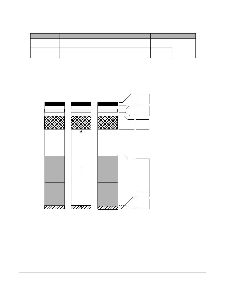
See Table 0-1 for names and versions of the referenced documents throughout the Device Guide.
Table 0-1 Document References
Since the device interfaces with several external industrial standards, please refer to the following for
details about those interface standards:
∑
"Information Technology - AT Attachment with Packet Interface - 5 (ATA/ATAPI5)," T13/1321D
rev 3, 29 February, 2000, ANSI.
∑
"CF+ and CompactFlash Specification," rev. 2.0 5/2003, CompactFlash Association.
User Guide
Version
Document Order
Number
HCS12 CPU Reference Manual
V02
S12CPUV2/D
HCS12 Breakpoint (BKP) Block Guide
V01
S12BKPV1/D
HCS12 Background Debug (BDM) Block Guide
V04
S12BDMV4/D
HCS12 Module Mapping Control (MMC) Block Guide
V04
S12MMCV4/D
HCS12 Multiplexed External Bus Interface (MEBI) Block Guide
V03
S12MEBIV3/D
HCS12 Interrupt (INT) Block Guide
V01
S12INTV1/D
Clock and Reset Generator (CRG_U) Block Guide
V01
S12CRGUV1/D
Timer: 16 bit, 8 channel (TIM_16B8C) Block Guide
V01
S12TIM16B8CV1/D
Serial Communications Interface (SCI) Block Guide
V04
S12SCIV4/D
32Kbyte Flash EEPROM (FTS32K) Block Guide
V01
S12FTS32KV1/D
Voltage Regulator (VREG_U) Block Guide
V01
S12VREGUV1/D
Oscillator (OSC) Block Guide
V02
S12OSCV2/D
Port Integration Module (PIM_9UF32) Block Guide
V02
S12UF32PIMV2/D
USB 2.0 Device Controller (USB20D6E2F) Block Guide
V01
S12USB20D6E2FV1/D
Integrated Queue Controller (IQUE) Block Guide
V01
S12IQUEV1/D
ATA5 Host Controller (ATA5HC) Block Guide
V01
S12ATA5HCV1/D
Smart Media Host Controller (SMHC) Block Guide
V01
S12SMHCV1/D
Secure Digital Host Controller (SDHC) Block Guide
V01
S12SDHCV1/D
Memory Stick Host Controller (MSHC) Block Guide
V01
S12MSHCV1/D
Compact Flash Host Controller (CFHC) Block Guide
V01
S12CFHCV1/D
SM RAM (SMRAM3P5K2E) Block Guide
V01
S12SMRAM3P5K2EV1/D

System on a Chip Guide -- 9S12UF32DGV1/D V01.05
18
Freescale Semiconductor
∑
"Memory Stick Information for Developers," ver. 1.3, 2000, Sony Corp.
∑
"The MultiMediaCard system specification," ver. 3.0, 1/2001, MMCA Technical Committee.
∑
"SD Memory Card Specifications," ver. 1.0, March 2000, SD Group.
∑
"Smart Media Electrical Specifications," ver. 1.0, May 19, 1999, SSFDC Forum Technical
Committee.
∑
"Universal Serial Bus Specification," rev. 2.0, 27 April 2000, Compaq, Hewlett-Packard, Intel,
Lucent, Microsoft, NEC, Philips.
Part Number
Figure 0-1
provides an ordering number example.
Figure 0-1 Order Part Number Coding
Table 0-2
lists the part number coding based on the package.
Table 0-2 Part Number Coding
Part Number
Package
Description
MC9S12UF32PB
64LQFP
MC9S12UF32
MC9S12UF32PU
100LQFP
MC9S12UF32
MC9S12 UF32 FU
Package Option
Device Title
Controller Family
Package Options
PU = 100LQFP
PB = 64LQFP

19
Freescale Semiconductor
System on a Chip Guide -- 9S12UF32DGV1/D V01.05
Section 1 Introduction
1.1 Overview
The MC9S12UF32 microcontroller unit (MCU) is USB2.0 device for memory card reader and
ATA/ATAPI interface applications. This device is composed of standard on-chip modules including a
16-bit central processing unit (HCS12 CPU), 32k bytes of Flash EEPROM, 3.5k bytes of RAM, USB2.0
interface, Integrated Queue Controller (IQUE) block with 1.5k bytes RAM buffer for USB Bulk data
transport, ATA5 interface, Compact Flash interface, SD/MMC interface, SmartMedia interface,
Memorystick interface, a 16-bit 8-channel timer, Serial Communication Interface, 73 discrete digital I/O
channels and 2 input only channels
1
. The MC9S12UF32 has full 16-bit internal data paths throughout.
1.2 Features
∑
HCS12 Core
≠
16-bit HCS12 CPU
i. Upward compatible with M68HC11 instruction set
ii. Interrupt stacking and programmer's model identical to M68HC11
iii. Instruction queue
iv. Enhanced indexed addressing
≠
Multiplexed External Bus Interface (MEBI)
≠
Memory Mapping Control (MMC)
≠
Interrupt Control (INT)
≠
Single-wire Background Debug Mode (BDM)
≠
On-chip hardware Breakpoints (BKP)
∑
Clock and Reset Generator (CRG_U)
≠
Clock Throttle to prescale the oscillator clock or 60Mhz clock from USB20D6E2F.
≠
COP watchdog
≠
Real Time Interrupt
∑
Memory
≠
32K Flash EEPROM
- Internal program/erase voltage generation
- Security and Block Protect bits
≠
3.5K byte RAM
NOTES
:
1. Not all functions are available simultaneously.

System on a Chip Guide -- 9S12UF32DGV1/D V01.05
20
Freescale Semiconductor
- Used as a contiguous 3.5k byte SRAM with misaligned access support
- Configurable to 1084 byte SRAM and 2000 x 10 bit SRAM for Smartmedia logical to physical
address translation and parity generation/checking support.
≠
1.5K byte Queue RAM
- SRAM used as USB endpoint buffer, access is arbitrated by IQUE module
∑
8-channel Timer (TIM)
≠
Eight input capture/output compare channels
≠
Clock prescaling
≠
16-bit counter
≠
16-bit pulse accumulator
∑
Serial Interface
≠
Asynchronous serial communication interface (SCI)
∑
Internal Regulator (VREG_U)
≠
Input voltage range from 4.25V to 5.5V
≠
Separate Regulation circuits
- 2.5V Regulator for Core Logic and memory
- 3.3V Regulator for USB2.0 physical layer interface
- 3.3V Regulator with off-chip NMOS driver for I/O and memory cards
≠
Power on Reset detection
∑
Integrated Queue Controller (IQUE)
≠
Provide block data transfer without CPU intervention
≠
Four independent queue channels for data transfer between Queue RAM and peripherals
≠
Unified Queue RAM Memory which can be allocated to different usb endpoints and storage
interface module
≠
Programming model allows implementation of double buffering for maximum burst data
throughput of 60M bytes per second between USB20D6E2F and one of the Storage Interfaces
∑
Universal Serial Bus 2.0 (USB20D6E2F)
≠
Intergrated USB2.0 Physical Layer Transceiver (USB20PHY) for High speed and Full Speed
operations
≠
USB 2.0 Serial Interface Engine (USB20SIE) for High Speed and Full Speed operations
compatible
- Endpoint 0 for Control IN and OUT operation
- Endpoint 2 and 3 are configurable for Bulk, ISO or Interrupt IN/OUT operation
- Endpoint buffer with programmable size residing in Queue RAM for endpoints 4 and 5

21
Freescale Semiconductor
System on a Chip Guide -- 9S12UF32DGV1/D V01.05
- Endpoint 0 IN, endpoint 0 OUT, endpoint 2 and endpoint 3 each has an independent 64 bytes
fixed endpoint buffer.
∑
ATA5 Host Controller Interface (ATA5HC)
≠
Support PIO mode 0 to 4
≠
Support Multi-word DMA mode 0 to 2
≠
Support UDMA mode 0 to 4 (Up to 60M Bytes/sec at UDMA mode 4)
≠
Sector data can be transferred to and from USB endpoint buffer without CPU intervention using
IQUE module
∑
Compact Flash Host Controller Interface (CFHC)
≠
Support Compact Flash memory and I/O mode access operations per CFA specification 1.4
≠
Sector data can be transferred to and from USB endpoint buffer without CPU intervention using
IQUE module
∑
Secure Digital and Multimedia Card Host Controller Interface (SDHC)
≠
Compatible with the MMC System Specification Version 3.0
≠
Compatible with the SD Memory Card Specification 1.0
≠
Sector data can be transferred to and from USB endpoint buffer without CPU intervention using
IQUE module
∑
Smartmedia Host Controller Interface (SMHC)
≠
Compatible with SmartMedia Specification 1.0
≠
Support SmartMedia with memory size of 4M Bytes to 128M Bytes
≠
Sector data can be transferred to and from USB endpoint buffer without CPU intervention using
IQUE module
∑
Memorystick Host Controller Interface (MSHC)
1
≠
Compatible with Memory Stick Standard 1.3
≠
Sector data can be transferred to and from USB endpoint buffer without CPU intervention using
IQUE module
∑
Two Asynchronous External Interrupt pins
≠
XIRQ
≠
IRQ
2
∑
100-Pin LQFP package
≠
Up to 6 I/O pins with 5V only drive capability and 2 input only 5V pins.
≠
Up to 67 I/O pins with 3.3V/5V input and drive capability.
NOTES
:
1. The Document for the Memory Stick Host Controller in the 912UF32 will be available to users who have obtained a formal
license of Memory Stick from Sony. Memory Stick is a Sony technology.
2. IRQ is not available in 64 pin device.

System on a Chip Guide -- 9S12UF32DGV1/D V01.05
22
Freescale Semiconductor
∑
64-Pin LQFP package
≠
User selectable subset of modules available.
≠
Up to 6 I/O pins with 5V only drive capability and 1 input only 5V pin.
≠
Up to 35 I/O pins with 3.3V/5V input and drive capability.
∑
Operating frequency
≠
Maximum 60MHz equivalent to 30MHz CPU Bus Speed for single chip modes.
≠
60MHz operation for IQUE module and storage interface modules attached to IQUE.
1.3 Modes of Operation
∑
Normal modes
≠
Normal Single-Chip Mode
≠
Normal Expanded Wide Mode
≠
Normal Expanded Narrow Mode
≠
Emulation Expanded Wide Mode
≠
Emulation Expanded Narrow Mode
∑
Special Operating Modes
≠
Special Single-Chip Mode with active Background Debug Mode
≠
Special Test Mode (Freescale use only)
≠
Special Peripheral Mode (Freescale use only)
∑
Each of the above modes of operation can be configured for two Low power sub-modes
≠
Stop Mode
≠
Wait Mode
∑
Secure operation, preventing the unauthorized read and write of the flash memory contents.

23
Freescale Semiconductor
System on a Chip Guide -- 9S12UF32DGV1/D V01.05
1.4 Block Diagram
Figure 1-1 MC9S12UF32 Block Diagram
32K Byte Flash EEPROM
3.5K Byte SMRAM
RESET
BKGD
R/W
MODB
XIRQ
NOACC
System
Integration
Module
(SIM)
VDDR
CPU12
Periodic Interrupt
COP Watchdog
Single-wire Background
Breakpoints
Multiplexed
Wide Bus
Multiplexed
Narrow Bus
IRQ
LSTRB
ECLK
MODA
PA
4
PA
3
PA
2
PA
1
PA
0
PA
7
PA
6
PA
5
TEST
ADDR12
ADDR11
ADDR10
ADDR9
ADDR8
ADDR15
ADDR14
ADDR13
D
A
T
A12
D
A
T
A11
D
A
T
A10
DA
T
A
9
DA
T
A
8
D
A
T
A15
D
A
T
A14
D
A
T
A13
PB4
PB3
PB2
PB1
PB0
PB7
PB6
PB5
ADDR4
ADDR3
ADDR2
ADDR1
ADDR0
ADDR7
ADDR6
ADDR5
DA
T
A
4
DA
T
A
3
DA
T
A
2
DA
T
A
1
DA
T
A
0
DA
T
A
7
DA
T
A
6
DA
T
A
5
DA
T
A
4
DA
T
A
3
DA
T
A
2
DA
T
A
1
DA
T
A
0
DA
T
A
7
DA
T
A
6
DA
T
A
5
PE3
PE4
PE5
PE6
PE7
PE0
PE1
PE2
IOC2
IOC6
IOC0
IOC7
IOC1
IOC3
IOC4
IOC5
PT3
PT0
PT1
PT2
PP3
PP4
PP5
PP0
PP1
PP2
PM3
PM4
PM5
PM0
PM1
PM2
PP6
PP7
PJ2
PQ1
PQ0
PQ2
PQ3
PQ4
PQ5
PQ6
PQ7
PJ0
PJ1
DDRA
DDRB
PTA
PTB
DDRE
PTE
PTT
DDRT
PTM
DDRM
PTP
DDRP
PTQ
DDRQ
PTJ
DDRJ
Clock and
Reset
Generation
Module
Voltage Regulator
VSSR
Debug Module
CMD
DAT2
DAT3
CLK
DAT0
DAT1
SDHC
BS
SDIO
SCLK
MSHC
VDDX
VSSX
I/O Driver 3.3/5V
VDDR
VSSR
Voltage Regulator 5V & I/O
Timer
SWP
SBSY
SALE
SDAT[0-7]
SCLE
SCE
SCD
SRE
SMHC
SWE
SCI
CFHC
Integrated
USB2.0
1.5K byte
Endpoint
Buffer
DPF
DMF
RPU
RREF
Queue
Module
PR3
PR4
PR5
PR6
PR7
PR0
PR1
PR2
PTR
DDRR
PS3
PS4
PS5
PS6
PS7
PS0
PS1
PS2
PTS
DDRS
PTU
DDRU
PU5
P
o
r
t
Multiple
x
e
r
USB2.0
Serial
Interface
Engine
Physical
Interface
VDD3X
VSS3X
I/O Driver 3.3/5V
VDD
PWROFF5V
PWROFF3V
(IQUE)
VDDA
VSSA
PHY Analog 3.3V
VDD
Internal Logic 2.5v
DPH
DMH
VREGEN
VDDA
REF3V
ATA5HC
PU3
PU4
PU0
PU1
PU2
RX
TX
(PHY)
(SIE)
IP-bus (30 MHz)*
FP-bus (60 MHz)
EXTAL
XTAL
Br
idge
Multiplexed Address/Data Bus
Port Multiplexer
* This block diagram shows only one particular module to port routing. Detail module routing for different
applications can be found in Signal Description Section.
* Some pins are not available in 100-pin package.
* IPbus runs at 1/2 frequency of S12 core bus, which is controlled by REFDV register of CRG_U module.
*Qbus refers to the data transfer channels between IQUE and USB/ATA5HC/CFHC/MSHC/SDHC/SMHC.
16
16
16
16
16
16
16
16
Q-bus (60MHz)

System on a Chip Guide -- 9S12UF32DGV1/D V01.05
24
Freescale Semiconductor
1.5 Device Memory Map
Table 1-1
shows the device memory map of the MC9S12UF32 after reset.
Table 1-1 Device Memory Map
Address
Module
Size
(Bytes)
Mapping
Register(s)
$0000 - $000F
HCS12 Multiplexed External Bus Interface
16
INITRG
$0010 - $0014
HCS12 Module Mapping Control
5
$0015 - $0016
HCS12 Interrupt
2
$0017 - $0018
Reserved
2
$0019 - $0019
Voltage Regulator (VREG_U)
1
$001A - $001B
Device ID register (PARTID)
2
$001C - $001D
HCS12 Module Mapping Control
2
$001E
HCS12 Multiplexed External Bus Interface
1
$001F
HCS12 Interrupt
1
$0020 - $0027
Reserved
8
$0028 - $002F
HCS12 Breakpoint
8
$0030 - $0033
Reserved
4
$0034 - $003F
Clock and Reset Generator (RTI, COP)
12
$0040 - $006F
Standard Timer 16-bit 8 channels (TIM)
48
$0070 - $00C7
Reserved
88
$00C8 - $00CF
Serial Communication Interface (SCI)
8
$00D0 - $00FF
Reserved
48
$0100 - $010F
Flash Control Register
16
$0110 - $011B
Reserved
12
$011C - $011F
RAM Control Register (SMRAM)
4
$0120 - $01BF
Reserved
160
$01C0- $01FF
ATA Host Controller (ATA5HC)
64
$0200 - $023F
Integrated Queue 4 channels (IQUE)
64
$0240 - $027F
Port Integration Module (PIM)
64
$0280 - $029F
CompactFlash Host Controller (CFHC)
32
$02A0 - $02AF
MemoryStick Host Controller (MSHC)
16
$02B0 - $02BF
SmartMedia Host Controller (SMHC)
16
$02C0 - $02DF
Secure Digital Host Controller (SDHC)
32
$02E0 - $02FF
Reserved
32
$0300 - $03FF
USB 2.0 (USB20D6E2F)
256
$0000 - $07FF
QRAM array (IQUE)
1.5K-byte 16-bit SRAM in IQUE module $0000 - $05FF
0.5K-byte reserved $0600-$07FF
2048
INITEE
1
$0800 - $1BC3
RAM array (SMRAM3P5K2E)
configurable as 2500-byte16-bit SRAM $1200 - $1BC3
or two 10-bit even byte aligned SRAM located at $0800 -
$0FCF and $1000 - $17CF
Unmapped locations in range $0800 - $1BC3 are reserved
5060
INITRM
$1BC4 - $1FFF
RAM array (SMRAM3P5K2E)
1084-byte 16-bit SRAM
1084
25
Freescale Semiconductor
System on a Chip Guide -- 9S12UF32DGV1/D V01.05
Figure 1-2 MC9S12UF32 Memory Map (Application Example)
$1800 - $3FFF
Reserved
10240
$4000 - $7FFF
16K-byte Flash EEPROM Array (addresses valid only when
ROMHM=0 of register MISC)
16384
PPAGE,
MISC
$8000 - $BFFF
16K-byte Paged Window
16384
$C000 - $FFFF
16K-byte Flash EEPROM Array
16384
NOTES
:
1. QRAM starting address is controlled by INITEE register and QRAM has the same priority as EEPROM mem-
ory block. For details about signal priority, please refer to HCS12 MMC Block Guide.
Table 1-1 Device Memory Map
VECTORS
$0000
$FFFF
$C000
$8000
$37FF
$0400
$2000
$FF00
EXT
NORMAL
SINGLE CHIP
EXPANDED
SPECIAL
SINGLE CHIP
$FF00
$FFFF
BDM
(If Active)
$FFFF
32K Fixed Flash EEPROM
$8000
$2000
$37FF
1K Bytes 16-bit RAM plus
Mappable to any 8K Boundary
$0000
$03FF
1K Register Space
Mappable to any 2K Boundary
The figure shows an example of an application memory map with the following register setting.
INITRG = $00
INITRM = $20
VECTORS
VECTORS
2.5K Bytes configurable RAM (see SMRAM)
$1000
$17FF
$1000
$17FF
1.5K QRAM Space plus
Mappable to any 2K Boundary
INITEE = $11
0.5K Reserved Space
PPAGE = $3E
This is not the map out of reset.
MISC = $0F
MISC = $0E
MISC = $0F

System on a Chip Guide -- 9S12UF32DGV1/D V01.05
26
Freescale Semiconductor
1.5.1 Detailed Register Map
$0000 - $000F
MEBI map 1 of 3 (HCS12 Multiplexed External Bus Interface)
Address
Name
Bit 7
Bit 6
Bit 5
Bit 4
Bit 3
Bit 2
Bit 1
Bit 0
$0000
PORTA
Read:
Bit 7
6
5
4
3
2
1
Bit 0
Write:
$0001
PORTB
Read:
Bit 7
6
5
4
3
2
1
Bit 0
Write:
$0002
DDRA
Read:
Bit 7
6
5
4
3
2
1
Bit 0
Write:
$0003
DDRB
Read:
Bit 7
6
5
4
3
2
1
Bit 0
Write:
$0004 -
$0007
Reserved
Read:
0
0
0
0
0
0
0
0
Write:
$0008
PORTE
Read:
Bit 7
6
5
4
3
2
Bit 1
Bit 0
Write:
$0009
DDRE
Read:
Bit 7
6
5
4
3
Bit 2
0
0
Write:
$000A
PEAR
Read:
NOACCE
0
PIPOE
NECLK
LSTRE
RDWE
0
0
Write:
$000B
MODE
Read:
MODC
MODB
MODA
0
IVIS
0
EMK
EME
Write:
$000C
PUCR
Read:
PUPKE
0
0
PUPEE
0
0
PUPBE
PUPAE
Write:
$000D
RDRIV
Read:
RDPK
0
0
RDPE
0
0
RDPB
RDPA
Write:
$000E
EBICTL
Read:
0
0
0
0
0
0
0
ESTR
Write:
$000F
Reserved
Read:
0
0
0
0
0
0
0
0
Write:
$0010 - $0014
MMC map 1 of 4 (HCS12 Module Mapping Control)
Address
Name
Bit 7
Bit 6
Bit 5
Bit 4
Bit 3
Bit 2
Bit 1
Bit 0
$0010
INITRM
Read:
RAM15
RAM14
RAM13
RAM12
RAM11
0
0
RAMHAL
Write:
$0011
INITRG
Read:
0
REG14
REG13
REG12
REG11
0
0
0
Write:
$0012
INITEE
Read:
EE15
EE14
EE13
EE12
EE11
0
0
EEON
Write:
$0013
MISC
Read:
0
0
0
0
EXSTR1 EXSTR0 ROMHM
ROMON
Write:
$0014
Reserved
Read:
0
0
0
0
0
0
0
0
Write:

27
Freescale Semiconductor
System on a Chip Guide -- 9S12UF32DGV1/D V01.05
$0015 - $0016
INT map 1 of 2 (HCS12 Interrupt)
Address
Name
Bit 7
Bit 6
Bit 5
Bit 4
Bit 3
Bit 2
Bit 1
Bit 0
$0015
ITCR
Read:
0
0
0
WRINT
ADR3
ADR2
ADR1
ADR0
Write:
$0016
ITEST
Read:
INTE
INTC
INTA
INT8
INT6
INT4
INT2
INT0
Write:
$0017 - $0017
MMC map 2 of 4 (HCS12 Module Mapping Control)
Address
Name
Bit 7
Bit 6
Bit 5
Bit 4
Bit 3
Bit 2
Bit 1
Bit 0
$0017
Reserved
Read:
0
0
0
0
0
0
0
0
Write:
$0018 - $0018
Reserved
Address
Name
Bit 7
Bit 6
Bit 5
Bit 4
Bit 3
Bit 2
Bit 1
Bit 0
$0018
Reserved
Read:
0
0
0
0
0
0
0
0
Write:
$0019 - $0019
VREG_U (Voltage Regulator)
Address
Name
Bit 7
Bit 6
Bit 5
Bit 4
Bit 3
Bit 2
Bit 1
Bit 0
$0019
Reserved for
factory testing
Read:
Write:
$001A - $001B
Device ID Register (Table 1-2)
Address
Name
Bit 7
Bit 6
Bit 5
Bit 4
Bit 3
Bit 2
Bit 1
Bit 0
$001A
PARTIDH
Read:
ID15
ID14
ID13
ID12
ID11
ID10
ID9
ID8
Write:
$001B
PARTIDL
Read:
ID7
ID6
ID5
ID4
ID3
ID2
ID1
ID0
Write:
$001C - $001D
MMC map 3 of 4 (HCS12 Module Mapping Control, Table 1-3)
Address
Name
Bit 7
Bit 6
Bit 5
Bit 4
Bit 3
Bit 2
Bit 1
Bit 0
$001C
MEMSIZ0
Read: reg_sw0
0
eep_sw1 eep_sw0
0
ram_sw2 ram_sw1 ram_sw0
Write:
$001D
MEMSIZ1
Read: rom_sw1 rom_sw0
0
0
0
0
pag_sw1 pag_sw0
Write:
$001E - $001E
MEBI map 2 of 3 (HCS12 Multiplexed External Bus Interface)
Address
Name
Bit 7
Bit 6
Bit 5
Bit 4
Bit 3
Bit 2
Bit 1
Bit 0
$001E
INTCR
Read:
IRQE
IRQEN
0
0
0
0
0
0
Write:

System on a Chip Guide -- 9S12UF32DGV1/D V01.05
28
Freescale Semiconductor
$001F - $001F
INT map 2 of 2 (HCS12 Interrupt)
Address
Name
Bit 7
Bit 6
Bit 5
Bit 4
Bit 3
Bit 2
Bit 1
Bit 0
$001F
HPRIO
Read:
PSEL7
PSEL6
PSEL5
PSEL4
PSEL3
PSEL2
PSEL1
0
Write:
$0020 - $0027
Reserved
Address
Name
Bit 7
Bit 6
Bit 5
Bit 4
Bit 3
Bit 2
Bit 1
Bit 0
$0020 -
$0027
Reserved
Read:
0
0
0
0
0
0
0
0
Write:
$0028 - $002F
BKP (HCS12 Breakpoint)
Address
Name
Bit 7
Bit 6
Bit 5
Bit 4
Bit 3
Bit 2
Bit 1
Bit 0
$0028
BKPCT0
Read:
BKEN
BKFULL
BKBDM
BKTAG
0
0
0
0
Write:
$0029
BKPCT1
Read:
BK0MBH BK0MBL BK1MBH BK1MBL BK0RWE
BK0RW
BK1RWE
BK1RW
Write:
$002A
BKP0X
Read:
0
0
BK0V5
BK0V4
BK0V3
BK0V2
BK0V1
BK0V0
Write:
$002B
BKP0H
Read:
Bit 15
14
13
12
11
10
9
Bit 8
Write:
$002C
BKP0L
Read:
Bit 7
6
5
4
3
2
1
Bit 0
Write:
$002D
BKP1X
Read:
0
0
BK1V5
BK1V4
BK1V3
BK1V2
BK1V1
BK1V0
Write:
$002E
BKP1H
Read:
Bit 15
14
13
12
11
10
9
Bit 8
Write:
$002F
BKP1L
Read:
Bit 7
6
5
4
3
2
1
Bit 0
Write:
$0030 - $0031
MMC map 4 of 4 (HCS12 Module Mapping Control)
Address
Name
Bit 7
Bit 6
Bit 5
Bit 4
Bit 3
Bit 2
Bit 1
Bit 0
$0030
Reserved
Read:
0
0
0
0
0
0
0
0
Write:
$0031
Reserved
Read:
0
0
0
0
0
0
0
0
Write:
$0032 - $0033
MEBI map 3 of 3 (HCS12 Multiplexed External Bus Interface)
Address
Name
Bit 7
Bit 6
Bit 5
Bit 4
Bit 3
Bit 2
Bit 1
Bit 0
$0032
Reserved
Read:
0
0
0
0
0
0
0
0
Write:
$0033
Reserved
Read:
0
0
0
0
0
0
0
0
Write:

29
Freescale Semiconductor
System on a Chip Guide -- 9S12UF32DGV1/D V01.05
$0034 - $003F
CRG_U (Clock and Reset Generator)
Address
Name
Bit 7
Bit 6
Bit 5
Bit 4
Bit 3
Bit 2
Bit 1
Bit 0
$0034
Reserved
Read:
0
0
0
0
0
0
0
0
Write:
$0035
REFDV
Read:
0
0
0
0
REFDV3 REFDV2 REFDV1 REFDV0
Write:
$0036
CTFLG
Test Only
Read:
TOUT7
TOUT6
TOUT5
TOUT4
TOUT3
TOUT2
TOUT1
TOUT0
Write:
$0037
CRGFLG
Read:
RTIF
PORF
0
LOCKIF
LOCK
0
0
0
Write:
$0038
CRGINT
Read:
RTIE
0
0
LOCKIE
0
0
0
0
Write:
$0039
CLKSEL
Read:
PLLSEL
0
SYSWAI ROAWAI
0
CWAI
RTIWAI
COPWAI
Write:
$003A
Reserved
Read:
0
0
0
0
0
0
0
0
Write:
$003B
RTICTL
Read:
0
RTR6
RTR5
RTR4
RTR3
RTR2
RTR1
RTR0
Write:
$003C
COPCTL
Read:
WCOP
RSBCK
0
0
0
CR2
CR1
CR0
Write:
$003D
FORBYP
Test Only
Read:
RTIBYP COPBYP
0
0
0
0
FCM
0
Write:
$003E
CTCTL
Test Only
Read:
TCTL7
TCTL6
TCTL5
TCTL4
TCLT3
TCTL2
TCTL1
TCTL0
Write:
$003F
ARMCOP
Read:
0
0
0
0
0
0
0
0
Write:
Bit 7
6
5
4
3
2
1
Bit 0
$0040 - $006F
TIM (Timer 16-Bit 8 Channels)
Address
Name
Bit 7
Bit 6
Bit 5
Bit 4
Bit 3
Bit 2
Bit 1
Bit 0
$0040
TIOS
Read:
IOS7
IOS6
IOS5
IOS4
IOS3
IOS2
IOS1
IOS0
Write:
$0041
CFORC
Read:
0
0
0
0
0
0
0
0
Write:
FOC7
FOC6
FOC5
FOC4
FOC3
FOC2
FOC1
FOC0
$0042
OC7M
Read:
OC7M7
OC7M6
OC7M5
OC7M4
OC7M3
OC7M2
OC7M1
OC7M0
Write:
$0043
OC7D
Read:
OC7D7
OC7D6
OC7D5
OC7D4
OC7D3
OC7D2
OC7D1
OC7D0
Write:
$0044
TCNT (hi)
Read:
Bit 15
14
13
12
11
10
9
Bit 8
Write:
$0045
TCNT (lo)
Read:
Bit 7
6
5
4
3
2
1
Bit 0
Write:
$0046
TSCR1
Read:
TEN
TSWAI
TSFRZ
TFFCA
0
0
0
0
Write:
$0047
TTOV
Read:
TOV7
TOV6
TOV5
TOV4
TOV3
TOV2
TOV1
TOV0
Write:
$0048
TCTL1
Read:
OM7
OL7
OM6
OL6
OM5
OL5
OM4
OL4
Write:
$0049
TCTL2
Read:
OM3
OL3
OM2
OL2
OM1
OL1
OM0
OL0
Write:

System on a Chip Guide -- 9S12UF32DGV1/D V01.05
30
Freescale Semiconductor
$004A
TCTL3
Read:
EDG7B
EDG7A
EDG6B
EDG6A
EDG5B
EDG5A
EDG4B
EDG4A
Write:
$004B
TCTL4
Read:
EDG3B
EDG3A
EDG2B
EDG2A
EDG1B
EDG1A
EDG0B
EDG0A
Write:
$004C
TIE
Read:
C7I
C6I
C5I
C4I
C3I
C2I
C1I
C0I
Write:
$004D
TSCR2
Read:
TOI
0
0
0
TCRE
PR2
PR1
PR0
Write:
$004E
TFLG1
Read:
C7F
C6F
C5F
C4F
C3F
C2F
C1F
C0F
Write:
$004F
TFLG2
Read:
TOF
0
0
0
0
0
0
0
Write:
$0050
TC0 (hi)
Read:
Bit 15
14
13
12
11
10
9
Bit 8
Write:
$0051
TC0 (lo)
Read:
Bit 7
6
5
4
3
2
1
Bit 0
Write:
$0052
TC1 (hi)
Read:
Bit 15
14
13
12
11
10
9
Bit 8
Write:
$0053
TC1 (lo)
Read:
Bit 7
6
5
4
3
2
1
Bit 0
Write:
$0054
TC2 (hi)
Read:
Bit 15
14
13
12
11
10
9
Bit 8
Write:
$0055
TC2 (lo)
Read:
Bit 7
6
5
4
3
2
1
Bit 0
Write:
$0056
TC3 (hi)
Read:
Bit 15
14
13
12
11
10
9
Bit 8
Write:
$0057
TC3 (lo)
Read:
Bit 7
6
5
4
3
2
1
Bit 0
Write:
$0058
TC4 (hi)
Read:
Bit 15
14
13
12
11
10
9
Bit 8
Write:
$0059
TC4 (lo)
Read:
Bit 7
6
5
4
3
2
1
Bit 0
Write:
$005A
TC5 (hi)
Read:
Bit 15
14
13
12
11
10
9
Bit 8
Write:
$005B
TC5 (lo)
Read:
Bit 7
6
5
4
3
2
1
Bit 0
Write:
$005C
TC6 (hi)
Read:
Bit 15
14
13
12
11
10
9
Bit 8
Write:
$005D
TC6 (lo)
Read:
Bit 7
6
5
4
3
2
1
Bit 0
Write:
$005E
TC7 (hi)
Read:
Bit 15
14
13
12
11
10
9
Bit 8
Write:
$005F
TC7 (lo)
Read:
Bit 7
6
5
4
3
2
1
Bit 0
Write:
$0060
PACTL
Read:
0
PAEN
PAMOD
PEDGE
CLK1
CLK0
PAOVI
PAI
Write:
$0061
PAFLG
Read:
0
0
0
0
0
0
PAOVF
PAIF
Write:
$0062
PACNT (hi)
Read:
Bit 7
6
5
4
3
2
1
Bit 0
Write:
$0040 - $006F
TIM (Timer 16-Bit 8 Channels)
Address
Name
Bit 7
Bit 6
Bit 5
Bit 4
Bit 3
Bit 2
Bit 1
Bit 0

31
Freescale Semiconductor
System on a Chip Guide -- 9S12UF32DGV1/D V01.05
$0063
PACNT (lo)
Read:
Bit 7
6
5
4
3
2
1
Bit 0
Write:
$0064
Reserved
Read:
0
0
0
0
0
0
0
0
Write:
$0065
Reserved
Read:
0
0
0
0
0
0
0
0
Write:
$0066
Reserved
Read:
0
0
0
0
0
0
0
0
Write:
$0067
Reserved
Read:
0
0
0
0
0
0
0
0
Write:
$0068
Reserved
Read:
0
0
0
0
0
0
0
0
Write:
$0069
Reserved
Read:
0
0
0
0
0
0
0
0
Write:
$006A
Reserved
Read:
0
0
0
0
0
0
0
0
Write:
$006B
Reserved
Read:
0
0
0
0
0
0
0
0
Write:
$006C
Reserved
Read:
0
0
0
0
0
0
0
0
Write:
$006D
Reserved
Read:
0
0
0
0
0
0
0
0
Write:
$006E
Reserved
Read:
0
0
0
0
0
0
0
0
Write:
$006F
Reserved
Read:
0
0
0
0
0
0
0
0
Write:
$0070 - $00C7
Reserved
Address
Name
Bit 7
Bit 6
Bit 5
Bit 4
Bit 3
Bit 2
Bit 1
Bit 0
$0070 -
$00C7
Reserved
Read:
0
0
0
0
0
0
0
0
Write:
$00C8 - $00CF
SCI (Asynchronous Serial Interface)
Address
Name
Bit 7
Bit 6
Bit 5
Bit 4
Bit 3
Bit 2
Bit 1
Bit 0
$00C8
SCIBDH
Read:
0
0
0
SBR12
SBR11
SBR10
SBR9
SBR8
Write:
$00C9
SCIBDL
Read:
SBR7
SBR6
SBR5
SBR4
SBR3
SBR2
SBR1
SBR0
Write:
$00CA
SCICR1
Read:
LOOPS
SCISWAI
RSRC
M
WAKE
ILT
PE
PT
Write:
$00CB
SCICR2
Read:
TIE
TCIE
RIE
ILIE
TE
RE
RWU
SBK
Write:
$00CC
SCISR1
Read:
TDRE
TC
RDRF
IDLE
OR
NF
FE
PF
Write:
$0040 - $006F
TIM (Timer 16-Bit 8 Channels)
Address
Name
Bit 7
Bit 6
Bit 5
Bit 4
Bit 3
Bit 2
Bit 1
Bit 0

System on a Chip Guide -- 9S12UF32DGV1/D V01.05
32
Freescale Semiconductor
$00CD
SCISR2
Read:
0
0
0
0
0
BRK13
TXDIR
RAF
Write:
$00CE
SCIDRH
Read:
R8
T8
0
0
0
0
0
0
Write:
$00CF
SCIDRL
Read:
R7
R6
R5
R4
R3
R2
R1
R0
Write:
T7
T6
T5
T4
T3
T2
T1
T0
$00D0 - $00FF
Reserved
Address
Name
Bit 7
Bit 6
Bit 5
Bit 4
Bit 3
Bit 2
Bit 1
Bit 0
$00D0 -
$00FF
Reserved
Read:
0
0
0
0
0
0
0
0
Write:
$0100 - $010F
Flash Control Register
Address
Name
Bit 7
Bit 6
Bit 5
Bit 4
Bit 3
Bit 2
Bit 1
Bit 0
$0100
FCLKDIV
Read: FDIVLD
PRDIV8
FDIV5
FDIV4
FDIV3
FDIV2
FDIV1
FDIV0
Write:
$0101
FSEC
Read: KEYEN1 KEYEN0
NV5
NV4
NV3
NV2
SEC1
SEC0
Write:
$0102
FTSTMOD
Read:
0
0
0
WRALL
0
0
0
0
Write:
$0103
FCNFG
Read:
CBEIE
CCIE
KEYACC
0
0
0
BKSEL1
BKSEL0
Write:
$0104
FPROT
Read:
FPOPEN
NV6
FPHDIS
FPHS1
FPHS0
FPLDIS
FPLS1
FPLS0
Write:
$0105
FSTAT
Read:
CBEIF
CCIF
PVIOL
ACCERR
0
BLANK
0
0
Write:
$0106
FCMD
Read:
0
CMDB6
CMDB5
0
0
CMDB2
0
CMDB0
Write:
$0107
Reserved for
Factory Test
Read:
0
0
0
0
0
0
0
0
Write:
$0108
Reserved for
Factory Test
Read:
0
0
0
0
0
0
0
0
Write:
$0109
Reserved for
Factory Test
Read:
0
0
0
0
0
0
0
0
Write:
$010A
Reserved for
Factory Test
Read:
0
0
0
0
0
0
0
0
Write:
$010B
Reserved for
Factory Test
Read:
0
0
0
0
0
0
0
0
Write:
$010C -
$010F
Reserved
Read:
0
0
0
0
0
0
0
0
Write:
$00C8 - $00CF
SCI (Asynchronous Serial Interface)
Address
Name
Bit 7
Bit 6
Bit 5
Bit 4
Bit 3
Bit 2
Bit 1
Bit 0

33
Freescale Semiconductor
System on a Chip Guide -- 9S12UF32DGV1/D V01.05
$0110 - $011B
Reserved
Address
Name
Bit 7
Bit 6
Bit 5
Bit 4
Bit 3
Bit 2
Bit 1
Bit 0
$0110 -
$011B
Reserved
Read:
0
0
0
0
0
0
0
0
Write:
$011C - $011F
SMRAM Control Register
Address
Name
Bit 7
Bit 6
Bit 5
Bit 4
Bit 3
Bit 2
Bit 1
Bit 0
$011C
SMRAMCFG
Read:
0
0
0
0
0
0
0
SMMODE
Write:
$011D
SMRAMSTAT
Read:
0
0
0
0
0
0
0
PSMBA
Write:
$011E -
$011F
Reserved
Read:
0
0
0
0
0
0
0
0
Write:
$0120 - $01BF
Reserved
Address
Name
Bit 7
Bit 6
Bit 5
Bit 4
Bit 3
Bit 2
Bit 1
Bit 0
$0120 -
$01BF
Reserved
Read:
0
0
0
0
0
0
0
0
Write:
$01C0 - $01FF
ATA Host Controller (ATA5HC)
Address
Name
Bit 7
Bit 6
Bit 5
Bit 4
Bit 3
Bit 2
Bit 1
Bit 0
$01C0
HCFG (hi)
Read:
SMR
FR
0
0
CLK_EN
XNW
IE
IORDY_E
N
Write:
$01C1
HCFG (lo)
Read:
0
0
0
0
0
0
0
0
Write:
$01C2
HSR (hi)
Read:
TIP
UREP
DRAB
0
FF
FE
RERR
WERR
Write:
$01C3
HSR (lo)
Read:
0
0
0
0
0
0
0
0
Write:
$01C4
HPIO1 (hi)
Read:
0
PIO_T0
Write:
$01C5
HPIO1 (lo)
Read:
0
0
PIO_T2_8
Write:
$01C6
HPIO2 (hi)
Read:
0
0
PIO_T2_16
Write:
$01C7
HPIO2 (lo)
Read:
0
0
0
0
PIO_T2I
Write:
$01C8
HPIO3 (hi)
Read:
0
0
0
0
0
PIO_T4
Write:
$01C9
HPIO3 (lo)
Read:
0
0
0
0
PIO_T1
Write:
$01CA
HPIO4 (hi)
Read:
0
0
0
0
0
PIO_TA
Write:
$01CB
HPIO4 (lo)
Read:
0
0
0
0
0
0
0
0
Write:

System on a Chip Guide -- 9S12UF32DGV1/D V01.05
34
Freescale Semiconductor
$01CC
HDMA1 (hi)
Read:
0
DMA_T0
Write:
$01CD
HDMA1 (lo)
Read:
0
0
DMA_TD
Write:
$01CE
HDMA2 (hi)
Read:
0
0
DMA_TK
Write:
$01CF
HDMA2 (lo)
Read:
0
0
0
0
DMA_TM
Write:
$01D0
HDMA3
(hi)
Read:
0
0
0
0
0
DMA_TH
Write:
$01D1
HDMA3
(lo)
Read:
0
0
0
0
0
DMA_TJ
Write:
$01D2
HDMA4 (hi)
Read:
0
0
0
0
0
DMA_TN
Write:
$01D3
HDMA4 (lo)
Read:
0
0
0
0
0
0
0
0
Write:
$01D4
HUDMA1 (hi)
Read:
0
0
UDMA_T2CYCTYP
Write:
$01D5
HUDMA1 (lo)
Read:
0
0
0
UDMA_TCYC
Write:
$01D6
HUDMA2 (hi)
Read:
0
0
0
0
0
UDMA_TDS
Write:
$01D7
HUDMA2 (lo)
Read:
0
0
0
0
0
UDMA_TDH
Write:
$01D8
HUDMA3
(hi)
Read:
0
0
0
UDMA_TDVS
Write:
$01D9
HUDMA3
(lo)
Read:
0
0
0
0
0
UDMA_TDVH
Write:
$01DA
HUDMA4 (hi)
Read:
0
0
UDMA_TFS
Write:
$01DB
HUDMA4 (lo)
Read:
0
0
TDMA_TU
Write:
$01DC
HUDMA5 (hi)
Read:
0
0
0
0
0
UDMA_TMLI
Write:
$01DD
HUDMA5 (lo)
Read:
0
0
0
0
0
UDMA_TAZ
Write:
$01DE
HUDMA6 (hi)
Read:
0
0
0
UDMA_TENV
Write:
$01DF
HUDMA6 (lo)
Read:
0
0
0
0
UDMA_TSR
Write:
$01E0
HUDMA7 (hi)
Read:
0
0
0
0
UDMA_TSS
Write:
$01E1
HUDMA7 (lo)
Read:
0
0
0
UDMA_TRFS
Write:
$01E2
HUDMA8 (hi)
Read:
0
0
UDMA_TRP
Write:
$01E3
HUDMA8 (lo)
Read:
0
0
0
0
0
UDMA_TACK
Write:
$01E4
HUDMA9 (hi)
Read:
0
0
0
0
0
UDMA_TZAH
Write:
$01C0 - $01FF
ATA Host Controller (ATA5HC)
Address
Name
Bit 7
Bit 6
Bit 5
Bit 4
Bit 3
Bit 2
Bit 1
Bit 0

35
Freescale Semiconductor
System on a Chip Guide -- 9S12UF32DGV1/D V01.05
$01E5
HUDMA9 (lo)
Read:
0
0
0
0
0
0
0
0
Write:
$01E6 -
$01ED
Reserved
Read:
0
0
0
0
0
0
0
0
Write:
$01EE
DCTR/DASR
1
(hi)
Read:
BSY
DRDY
#
DRQ
obs
ERR
Write:
SRST
nIEN
ZERO
$01EF
DCTR/DASR
1
(lo)
Read:
0
0
0
0
0
0
0
0
Write:
$01F0
DDR (hi)
1
Read:
BYTE_E
Write:
$01F1
DDR (lo)
1
Read:
BYTE_O
Write:
$01F2
DFR/DER (hi)
1
Read:
#r1
ABRT
#r2
Write:
#w
$01F3
DFR/DER (lo)
1
Read:
0
0
0
0
0
0
0
0
Write:
$01F4
DSCR (hi)
1
Read:
#
Write:
$01F5
DSCR (lo)
1
Read:
0
0
0
0
0
0
0
0
Write:
$01F6
DSNR (hi)
1
Read:
#
Write:
$01F7
DSNR (lo)
1
Read:
0
0
0
0
0
0
0
0
Write:
$01F8
DCLR (hi)
1
Read:
#
Write:
$01F9
DCLR (lo)
1
Read:
0
0
0
0
0
0
0
0
Write:
$01FA
DCHR (hi)
1
Read:
#
Write:
$01FB
DCHR (lo)
1
Read:
0
0
0
0
0
0
0
0
Write:
$01FC
DDHR (hi)
1
Read:
obs
#1
obs
DEV
#2
Write:
$01FD
DDHR (lo)
1
Read:
0
0
0
0
0
0
0
0
Write:
$01FE
DCR/DSR (hi)
1
Read:
BSY
DRDY
#r
DRQ
obs
ERR
Write:
#w
$01FF
HDMAM (lo)
Read:
PIE
HUT
AF
0
IE
UDMA
RD
WR
Write:
NOTES
:
1. These registers are mapped to the registers on an external ATA/ATAPI device, for detail explanation of the #, #r1,
#r2, #w, #1,#2 field, please refer to the ATAHC block guide and ATA/ATAPI standards.
$01C0 - $01FF
ATA Host Controller (ATA5HC)
Address
Name
Bit 7
Bit 6
Bit 5
Bit 4
Bit 3
Bit 2
Bit 1
Bit 0

System on a Chip Guide -- 9S12UF32DGV1/D V01.05
36
Freescale Semiconductor
$0200 - $023F
IQUE (Integrated Queue Module)
Address
Name
Bit 7
Bit 6
Bit 5
Bit 4
Bit 3
Bit 2
Bit 1
Bit 0
$0200
IQUECR
Read:
0
0
0
QC34DBE QC12DBE
0
0
IQUEEN
Write:
IQUERST
$0201
Reserved
Read:
0
0
0
0
0
0
0
0
Write:
$0202
QC1DR (hi)
Read:
Q1DATA
Write:
$0203
QC1DR (lo)
Read:
Q1DATA
Write:
$0204
QC1BP (hi)
Read:
0
0
0
0
BEGPTR
Write:
$0205
QC1BP (lo)
Read:
BEGPTR
Write:
$0206
QC1EP (hi)
Read:
0
0
0
0
ENDPTR
Write:
$0207
QC1EP (lo)
Read:
ENDPTR
Write:
$0208
QC1CR
Read:
Q1VIE
Q1EIE
Q1FIE
Q1EN
Q1SML
Q116EN Q1THRU
0
Write:
Q1PRST
$0209
QC1SR
Read:
Q1VSF
Q1FSF
Q1ESF
Q1VIF
Q1FIF
Q1EIF
0
0
Write:
0
0
0
$020A
QC1SZB
Read:
QSIZE
QBASE
Write:
$020B
QC1REQ
Read:
0
0
0
0
Q1REQ
Write:
$020C
QC2DR (hi)
Read:
Q2DATA
Write:
$020D
QC2DR (lo)
Read:
Q2DATA
Write:
$020E
QC2BP (hi)
Read:
0
0
0
0
BEGPTR
Write:
$020F
QC2BP (lo)
Read:
BEGPTR
Write:
$0210
QC2EP (hi)
Read:
0
0
0
0
ENDPTR
Write:
$0211
QC2EP (lo)
Read:
ENDPTR
Write:
$0212
QC2CR
Read:
Q2VIE
Q2EIE
Q2FIE
Q2EN
Q2SML
Q216EN Q2THRU
0
Write:
Q2PRST
$0213
QC2SR
Read:
Q2VSF
Q2FSF
Q2ESF
Q2VIF
Q2FIF
Q2EIF
0
0
Write:
0
0
0
$0214
QC2SZB
Read:
QSIZE
QBASE
Write:
$0215
QC2REQ
Read:
0
0
0
0
Q2REQ
Write:
$0216
QC3DR (hi)
Read:
Q3DATA
Write:
$0217
QC3DR (lo)
Read:
Q3DATA
Write:
$0218
QC3BP (hi)
Read:
0
0
0
0
BEGPTR
Write:

37
Freescale Semiconductor
System on a Chip Guide -- 9S12UF32DGV1/D V01.05
$0219
QC3BP (lo)
Read:
BEGPTR
Write:
$021A
QC3EP (hi)
Read:
0
0
0
0
ENDPTR
Write:
$021B
QC3EP (lo)
Read:
ENDPTR
Write:
$021C
QC3CR
Read:
Q3VIE
Q3EIE
Q3FIE
Q3EN
Q3SML
Q316EN Q3THRU
0
Write:
Q3PRST
$021D
QC3SR
Read:
Q3VSF
Q3FSF
Q3ESF
Q3VIF
Q3FIF
Q3EIF
0
0
Write:
0
0
0
$021E
QC3SZB
Read:
QSIZE
QBASE
Write:
$021F
QC3REQ
Read:
0
0
0
0
Q3REQ
Write:
$0220
QC4DR (hi)
Read:
Q4DATA
Write:
$0221
QC4DR (lo)
Read:
Q4DATA
Write:
$0222
QC4BP (hi)
Read:
0
0
0
0
BEGPTR
Write:
$0223
QC4BP (lo)
Read:
BEGPTR
Write:
$0224
QC4EP (hi)
Read:
0
0
0
0
ENDPTR
Write:
$0225
QC4EP (lo)
Read:
ENDPTR
Write:
$0226
QC4CR
Read:
Q4VIE
Q4EIE
Q4FIE
Q4EN
Q4SML
Q416EN Q4THRU
0
Write:
Q4PRST
$0227
QC4SR
Read:
Q4VSF
Q4FSF
Q4ESF
Q4VIF
Q4FIF
Q4EIF
0
0
Write:
0
0
0
$0228
QC4SZB
Read:
QSIZE
QBASE
Write:
$0229
QC4REQ
Read:
0
0
0
0
Q4REQ
Write:
$022A
QC12DCR
Read:
0
0
0
SBTE
DBTIE
DBEIE
DBFIE
0
Write:
DBRST
$022B
QC34DCR
Read:
0
0
0
SBTE
DBTIE
DBEIE
DBFIE
0
Write:
DBRST
$022C
QC12DSR
Read:
DBTCIF
DBEIF
DBFIF
0
0
0
DBSF
Write:
$022D
QC34DSR
Read:
DBTCIF
DBEIF
DBFIF
0
0
0
DBSF
Write:
$022E
QCDCT (hi)
Read:
DBTRAN34
Write:
$022F
QCDCT (lo)
Read:
DBTRAN12
Write:
$0200 - $023F
IQUE (Integrated Queue Module)
Address
Name
Bit 7
Bit 6
Bit 5
Bit 4
Bit 3
Bit 2
Bit 1
Bit 0
System on a Chip Guide -- 9S12UF32DGV1/D V01.05
38
Freescale Semiconductor
$0230
QC12DSHR
Read:
0
0
0
0
0
0
DRHE
DTHE
Write:
RXDF
RXDA
TXRD
TXDA
$0231
QC34DSHR
Read:
0
0
0
0
0
0
DRHE
DTHE
Write:
RXDF
RXDA
TXRD
TXDA
$0232 -
$023F
Reserved
Read:
0
0
0
0
0
0
0
0
Write:
$0240 - $027F
PIM (Port Integration Module PIM_9UF32)
Address
Name
Bit 7
Bit 6
Bit 5
Bit 4
Bit 3
Bit 2
Bit 1
Bit 0
$0240
PTT
Read:
0
0
0
0
PTT3
PTT2
PTT1
PTT0
Write:
$0241
PTIT
Read:
0
0
0
0
PTIT3
PTIT2
PTIT1
PTIT0
Write:
$0242
DDRT
Read:
0
0
0
0
DDRT3
DDRT2
DDRT1
DDRT0
Write:
$0243
RDRT
Read:
0
0
0
0
RDRT3
RDRT2
RDRT1
RDRT0
Write:
$0244
PERT
Read:
0
0
0
0
PERT3
PERT2
PERT1
PERT0
Write:
$0245
PPST
Read:
0
0
0
0
PPST3
PPST2
PPST1
PPST0
Write:
$0246 -
$0247
Reserved
Read:
0
0
0
0
0
0
0
0
Write:
$0248
PTM
Read:
0
0
PTM5
PTM4
PTM3
PTM2
PTM1
PTM0
Write:
$0249
PTIM
Read:
0
0
PTIM5
PTIM4
PTIM3
PTIM2
PTIM1
PTIM0
Write:
$024A
DDRM
Read:
0
0
DDRM5
DDRM4
DDRM3
DDRM2
DDRM1
DDRM0
Write:
$024B
RDRM
Read:
0
0
RDRM5
RDRM4
RDRM3
RDRM2
RDRM1
RDRM0
Write:
$024C
PERM
Read:
0
0
PERM5
PERM4
PERM3
PERM2
PERM1
PERM0
Write:
$024D
PPSM
Read:
0
0
PPSM5
PPSM4
PPSM3
PPSM2
PPSM1
PPSM0
Write:
$024E -
$024F
Reserved
Read:
0
0
0
0
0
0
0
0
Write:
$0250
PTJ
Read:
0
0
0
0
0
PTJ2
PTJ1
PTJ0
Write:
$0251
PTIJ
Read:
0
0
0
0
0
PTIJ2
PTIJ1
PTIJ0
Write:
$0252
DDRJ
Read:
0
0
0
0
0
DDRJ2
DDRJ1
DDRJ0
Write:
$0253
RDRJ
Read:
0
0
0
0
0
RDRJ2
RDRJ1
RDRJ0
Write:
$0254
PERJ
Read:
0
0
0
0
0
PERJ2
PERJ1
PERJ0
Write:
$0200 - $023F
IQUE (Integrated Queue Module)
Address
Name
Bit 7
Bit 6
Bit 5
Bit 4
Bit 3
Bit 2
Bit 1
Bit 0

39
Freescale Semiconductor
System on a Chip Guide -- 9S12UF32DGV1/D V01.05
$0255
PPSJ
Read:
0
0
0
0
0
PPSJ2
PPSJ1
PPSJ0
Write:
$0256
Reserved
Read:
0
0
0
0
0
0
0
0
Write:
$0257
MODRR
Read:
0
0
0
MODRR4 MODRR3 MODRR2 MODRR1 MODRR0
Write:
$0258
PTP
Read:
PTP7
PTP6
PTP5
PTP4
PTP3
PTP2
PTP1
PTP0
Write:
$0259
PTIP
Read:
PTIP7
PTIP6
PTIP5
PTIP4
PTIP3
PTIP2
PTIP1
PTIP0
Write:
$025A
DDRP
Read:
DDRP7
DDRP7
DDRP5
DDRP4
DDRP3
DDRP2
DDRP1
DDRP0
Write:
$025B
RDRP
Read:
RDRP7
RDRP6
RDRP5
RDRP4
RDRP3
RDRP2
RDRP1
RDRP0
Write:
$025C
PERP
Read:
PERP7
PERP6
PERP5
PERP4
PERP3
PERP2
PERP1
PERP0
Write:
$025D
PPSP
Read:
PPSP7
PPSP6
PPSP5
PPSP4
PPSP3
PPSP2
PPSP1
PPSS0
Write:
$025E -
$025F
Reserved
Read:
0
0
0
0
0
0
0
0
Write:
$0260
PTQ
Read:
PTQ7
PTQ6
PTQ5
PTQ4
PTQ3
PTQ2
PTQ1
PTQ0
Write:
$0261
PTIQ
Read:
PTIQ7
PTIQ6
PTIQ5
PTIQ4
PTIQ3
PTIQ2
PTIQ1
PTIQ0
Write:
$0262
DDRQ
Read:
DDRQ7
DDRQ7
DDRQ5
DDRQ4
DDRQ3
DDRQ2
DDRQ1
DDRQ0
Write:
$0263
RDRQ
Read:
RDRQ7
RDRQ6
RDRQ5
RDRQ4
RDRQ3
RDRQ2
RDRQ1
RDRQ0
Write:
$0264
PERQ
Read:
PERQ7
PERQ6
PERQ5
PERQ4
PERQ3
PERQ2
PERQ1
PERQ0
Write:
$0265
PPSQ
Read:
PPSQ7
PPSQ6
PPSQ5
PPSQ4
PPSQ3
PPSQ2
PPSQ1
PPSQ0
Write:
$0266 -
$0267
Reserved
Read:
0
0
0
0
0
0
0
0
Write:
$0268
PTR
Read:
PTR7
PTR6
PTR5
PTR4
PTR3
PTR2
PTR1
PTR0
Write:
$0269
PTIR
Read:
PTIR7
PTIR6
PTIR5
PTIR4
PTIR3
PTIR2
PTIR1
PTIR0
Write:
$026A
DDRR
Read:
DDRR7
DDRR7
DDRR5
DDRR4
DDRR3
DDRR2
DDRR1
DDRR0
Write:
$026B
RDRR
Read:
RDRR7
RDRR6
RDRR5
RDRR4
RDRR3
RDRR2
RDRR1
RDRR0
Write:
$026C
PERR
Read:
PERR7
PERR6
PERR5
PERR4
PERR3
PERR2
PERR1
PERR0
Write:
$026D
PPSR
Read:
PPSR7
PPSR6
PPSR5
PPSR4
PPSR3
PPSR2
PPSR1
PPSR0
Write:
$026E -
$026F
Reserved
Read:
0
0
0
0
0
0
0
0
Write:
$0270
PTS
Read:
PTS7
PTS6
PTS5
PTS4
PTS3
PTS2
PTS1
PTS0
Write:
$0240 - $027F
PIM (Port Integration Module PIM_9UF32)
Address
Name
Bit 7
Bit 6
Bit 5
Bit 4
Bit 3
Bit 2
Bit 1
Bit 0

System on a Chip Guide -- 9S12UF32DGV1/D V01.05
40
Freescale Semiconductor
$0271
PTIS
Read:
PTIS7
PTIS6
PTIS5
PTIS4
PTIS3
PTIS2
PTIS1
PTIS0
Write:
$0272
DDRS
Read:
DDRS7
DDRS7
DDRS5
DDRS4
DDRS3
DDRS2
DDRS1
DDRS0
Write:
$0273
RDRS
Read:
RDRS7
RDRS6
RDRS5
RDRS4
RDRS3
RDRS2
RDRS1
RDRS0
Write:
$0274
PERS
Read:
PERS7
PERS6
PERS5
PERS4
PERS3
PERS2
PERS1
PERS0
Write:
$0275
PPSS
Read:
PPSS7
PPSS6
PPSS5
PPSS4
PPSS3
PPSS2
PPSS1
PPSS0
Write:
$0276 -
$0277
Reserved
Read:
0
0
0
0
0
0
0
0
Write:
$0278
PTU
Read:
0
0
PTU5
PTU4
PTU3
PTU2
PTU1
PTU0
Write:
$0279
PTIU
Read:
0
0
PTIU5
PTIU4
PTIU3
PTIU2
PTIU1
PTIU0
Write:
$027A
DDRU
Read:
0
0
DDRU5
DDRU4
DDRU3
DDRU2
DDRU1
DDRU0
Write:
$027B
RDRU
Read:
0
0
RDRU5
RDRU4
RDRU3
RDRU2
RDRU1
RDRU0
Write:
$027C
PERU
Read:
0
0
PERU5
PERU4
PERU3
PERU2
PERU1
PERU0
Write:
$027D
PPSU
Read:
0
0
PPSU5
PPSU4
PPSU3
PPSU2
PPSU1
PPSU0
Write:
$027E -
$027F
Reserved
Read:
0
0
0
0
0
0
0
0
Write:
$0280 - $029F
CFHC (Compact Flash Host Controller)
Address
Name
Bit 7
Bit 6
Bit 5
Bit 4
Bit 3
Bit 2
Bit 1
Bit 0
$0280
CFISR (hi)
Read:
0
0
0
0
0
0
VCC
CWAIT
Write:
$0281
CFISR (lo)
Read: INPACK
VS
RDY
IOIS16
CD2
CD1
SPKRB
CHG
Write:
$0282
CFCCR (hi)
Read:
0
0
0
0
0
0
0
0
Write:
$0283
CFCCR (lo)
Read:
0
0
0
0
CE2B
CE1B
REGB
COM
Write:
$0284
CFSCR1 (hi)
Read:
CFE
CFOE
CRST
DISINC
CFSWAI
IEDGE
WERRIE
TERRIE
Write:
$0285
CFSCR1 (lo)
Read:
CFRFIE
CFTEIE
OOIE
CIE
VSIE
RDYIE
CHGIE
CDIE
Write:
$0286
CFSCR2 (hi)
Read:
CA10E
CA9E
CA8E
CA7E
CA6E
CA5E
CA4E
0
Write:
$0287
CFSCR2 (lo)
Read:
0
0
TPS5-TPS0
Write:
$0288
CFCR (hi)
Read:
0
0
0
0
0
0
0
0
Write:
$0240 - $027F
PIM (Port Integration Module PIM_9UF32)
Address
Name
Bit 7
Bit 6
Bit 5
Bit 4
Bit 3
Bit 2
Bit 1
Bit 0

41
Freescale Semiconductor
System on a Chip Guide -- 9S12UF32DGV1/D V01.05
$0289
CFCR (lo)
Read:
HIS
BSY
0
TQ
RQ
STOP
0
RWB
Write:
INVOKE
$028A
CFBBAR (hi)
Read:
0
0
0
0
0
BBA10-BBA8
Write:
$028B
CFBBAR (lo)
Read:
BBA7-BBA0
Write:
$028C
CFBSR (hi)
Read:
0
0
0
0
0
0
0
0
Write:
BS8
$028D
CFBSR (lo)
Read:
0
0
0
0
0
0
0
0
Write:
BS7
BS6
BS5
BS4
BS3
BS2
BS1
BS0
$028E
CFPMR (hi)
Read:
0
0
0
0
0
0
0
0
Write:
$028F
CFPMR (lo)
Read:
0
0
0
0
0
0
CPE
CVS
Write:
$0290
CFDR (hi)
Read:
RD15-RD8
Write:
TD15-TD8
$0291
CFDR (lo)
Read:
RD7-RD0
Write:
TD7-TD0
$0292
CFIFR (hi)
Read:
0
0
0
0
0
0
WERRIF
TERRIF
Write:
$0293
CFIFR (lo)
Read: CFRFIF
CFTEIF
OOIF
CIF
VSIF
RDYIF
CHGIF
CDIF
Write:
0
$0294 -
$029F
Reserved
Read:
0
0
0
0
0
0
0
0
Write:
$02A0 - $02AF
MSHC (Memory Stick Host Controller)
Address
Name
Bit 7
Bit 6
Bit 5
Bit 4
Bit 3
Bit 2
Bit 1
Bit 0
$02A0
MSCMD (hi)
Read:
PID
0
0
DATASIZE9-8
Write:
$02A1
MSCMD (lo)
Read:
DATASIZE7-0
Write:
$02A2
MSC0
Read:
RST
PWS
SIEN
MSCE
NOCRC
BSYCNT
Write:
$02A3
MSS0
Read:
0
0
0
0
RBE
RBF
TBE
TBF
Write:
$02A4
MSTDATA (hi)
Read:
0
0
0
0
0
0
0
0
Write:
TX DATA BUFFER 15-8
$02A5
MSTDATA (lo)
Read:
0
0
0
0
0
0
0
0
Write:
TX DATA BUFFER 7-0
$02A6
MSRDATA (hi)
Read:
RX DATA BUFFER 15-8
Write:
0
0
0
0
0
0
0
0
$02A7
MSRDATA (lo)
Read:
RX DATA BUFFER 7-0
Write:
0
0
0
0
0
0
0
0
$02A8
MSIC
Read:
INTE
DTRQIE
DTCMPIE
FAEEN
0
0
0
0
Write:
$02A9
MSIS
Read:
RDY
SIF
DTRQ
DTCMP
0
FAE
CRCE
TOE
Write:
$0280 - $029F
CFHC (Compact Flash Host Controller)
Address
Name
Bit 7
Bit 6
Bit 5
Bit 4
Bit 3
Bit 2
Bit 1
Bit 0

System on a Chip Guide -- 9S12UF32DGV1/D V01.05
42
Freescale Semiconductor
$02AA
MSC1
Read:
ACD
0
DIV
DTRQE
0
RFF
TFE
Write:
$02AB
MSS1
Read:
RUN
TOV
0
0
0
0
0
0
Write:
$02AC
MSACMD (hi)
Read:
APID
0
0
ADATASIZE9-8
Write:
$02AD
MSACMD (lo)
Read:
ADATASIZE7-0
Write:
$02AE
Reserved
Read:
0
0
0
0
0
0
0
0
Write:
$02AF
Reserved
Read:
0
0
0
0
0
0
0
0
Write:
$02B0 - $02BF
SMHC (Smart Media Host Controller)
Address
Name
Bit 7
Bit 6
Bit 5
Bit 4
Bit 3
Bit 2
Bit 1
Bit 0
$02B0
SMC
Read:
0
SMHCEN
FRST
SMRST
QEN
ECCEN
CNT1
CNT0
Write:
$02B1
SMHS
Read:
0
0
0
0
0
0
0
0
Write:
SCE
$02B2
SMTDATA/
SMRDATA (hi)
Read:
Rx DATA BUFFER 15-8
Write:
Tx DATA BUFFER 15-8
$02B3
SMTDATA/
SMRDATA (lo)
Read:
Rx DATA BUFFER 7-0
Write:
Tx DATA BUFFER 7-0
$02B4
SMISR
Read:
0
HCE
ECCR
RDR
RDP
CDIN
CDOUT
RDY
Write:
$02B5
SMIMR
Read:
INTEN
HCEIEN
ECCRIEN
RDRIEN
RDPIEN CDINIEN
CDOUTIEN
RDYIEN
Write:
$02B6
SMS
Read:
0
CEC
SME
BAF2P
BAF1P
DRQ
BUSY
CP
Write:
$02B7
SMFCS
Read:
0
0
RFL
TFL
RBE
RBF
TBE
TBF
Write:
$02B8
SMCLKR
Read:
0
0
0
0
0
PS2
PS1
PS0
Write:
$02B9 -
$02BF
Reserved
Read:
0
0
0
0
0
0
0
0
Write:
$02C0 - $02DF
SDHC (Secure Digital Host Controller)
Address
Name
Bit 7
Bit 6
Bit 5
Bit 4
Bit 3
Bit 2
Bit 1
Bit 0
$02C0
SDCON (hi)
Read:
0
0
0
0
0
0
0
0
Write:
$02C1
SDCON (lo)
Read:
0
0
LBUF
IRST
PUEN
PDEN
QIEN
SDEN
Write:
$02C2
SDSTAT (hi)
Read:
0
BLK_RDY
FFULL
FEMPTY
CD
ECR
WRDN
DTDN
Write:
$02C3
SDSTAT (lo)
Read: SDCKON WR_ECRC_NODE
RSP_ECRC
RD_ECRC
WR_ECRC
RSPTO
RDTO
Write:
$02A0 - $02AF
MSHC (Memory Stick Host Controller)
Address
Name
Bit 7
Bit 6
Bit 5
Bit 4
Bit 3
Bit 2
Bit 1
Bit 0

43
Freescale Semiconductor
System on a Chip Guide -- 9S12UF32DGV1/D V01.05
$02C4
SDCLKCON
(hi)
Read:
0
0
0
0
0
0
0
0
Write:
$02C5
SDCLKCON
(lo)
Read:
0
0
0
0
SCLKEN
CLKRATE
Write:
$02C6
SDCMDATCO
N (hi)
Read:
0
0
0
0
0
NOBEN
WBUS
0
Write:
$02C7
SDCMDATCO
N (lo)
Read:
INIT
BUSY
MBLK
SBMOD
WRD
DATAEN
RSPNO
Write:
$02C8
SDRTOUT (hi)
Read:
0
0
0
0
0
0
0
0
Write:
$02C9
SDRTOUT (lo)
Read:
0
RSP_TO
Write:
$02CA
SDRDTOUT
(hi)
Read:
RD_TO 15-8
Write:
$02CB
SDRDTOUT
(lo)
Read:
RD_TO 7-0
Write:
$02CC
SDBLKLN (hi)
Read:
0
0
0
0
0
0
BLEN9
BLEN8
Write:
$02CD
SDBLKLN (lo)
Read:
BLEN 7-0
Write:
$02CE
SDNOBLK (hi)
Read:
NOB 15-8
Write:
$02CF
SDNOBLK (lo)
Read:
NOB 7-0
Write:
$02D0
SDINTREN
(hi)
Read:
0
0
0
0
0
0
0
0
Write:
$02D1
SDINTREN
(lo)
Read:
0
0
CDIE
ECRIE
WRDNIE DTDNIE
CRCIE
TOIE
Write:
$02D2
SDCMDNO
(hi)
Read:
0
0
0
0
0
0
0
0
Write:
$02D3
SDCMDNO
(lo)
Read:
0
0
CMDNO
Write:
$02D4
SDARGH (hi)
Read:
HARG 15-8
Write:
$02D5
SDARGH (lo)
Read:
HARG 7-0
Write:
$02D6
SDARGL (hi)
Read:
LARG 15-8
Write:
$02D7
SDARGL (lo)
Read:
LARG 7-0
Write:
$02D8
SDRSP (hi)
Read:
CRSP 15-8
Write:
$02D9
SDRSP (lo)
Read:
CRSP 7-0
Write:
$02DA
SDATA (hi)
Read:
SDAT 15-8
Write:
$02DB
SDATA (lo)
Read:
SDAT 7-0
Write:
$02DC -
$02DF
Reserved
Read:
0
0
0
0
0
0
0
0
Write:
$02C0 - $02DF
SDHC (Secure Digital Host Controller)
Address
Name
Bit 7
Bit 6
Bit 5
Bit 4
Bit 3
Bit 2
Bit 1
Bit 0

System on a Chip Guide -- 9S12UF32DGV1/D V01.05
44
Freescale Semiconductor
$02E0 - $02FF
Reserved
Address
Name
Bit 7
Bit 6
Bit 5
Bit 4
Bit 3
Bit 2
Bit 1
Bit 0
$02E0 -
$02FF
Reserved
Read:
0
0
0
0
0
0
0
0
Write:
$0300 - $03FF
USB20D6E2F (Universal Serial Bus 2.0 Device Controller)
Address
Name
Bit 7
Bit 6
Bit 5
Bit 4
Bit 3
Bit 2
Bit 1
Bit 0
$0300
UMCR (hi)
Read:
MEN
MCE
0
RESUME
SPHY
0
0
0
Write:
MRST
PHYRST
EPRST
$0301
UMCR (lo)
Read:
0
0
DISCON
SDSUP
EXSPD
RWUC
SPWR
SCSUP
Write:
$0302
UMSR1 (hi)
Read:
ACTEP
USSC
URSC
ENUMD
0
0
Write:
$0303
UMSR1 (lo)
Read:
0
SPD
0
USD
URD
SOF
SETOVR
SETUP
Write:
$0304
UIMR (hi)
Read:
0
RESUMEIE
SETECRIE
USSCIE
URSCIE
0
0
0
Write:
$0305
UIMR (lo)
Read:
0
0
0
0
0
SOFIE
SETOVRIE
SETUPIE
Write:
$0306
Reserved
Read:
0
0
0
0
0
0
0
0
Write:
$0307
Reserved
Read:
0
0
0
0
0
0
0
0
Write:
$0308
Reserved for
Factory Testing
Read:
Write:
$0309
Reserved for
Factory Testing
Read:
Write:
$030A
UTSR (hi)
Read:
0
0
0
0
0
TIMEST 10-8
Write:
$030B
UTSR (lo)
Read:
TIMEST 7-0
Write:
$030C
UCCSR (hi)
Read:
CFGVALID
INTFVALID
SETECR
DONE-
ECRU
CFG
Write:
$030D
UCCSR (lo)
Read:
INTF
ALTINTF
Write:
$030E
UEPCSELR (hi)
Read:
0
0
0
0
UCRSEL
Write:
$030F
UEPCSELR (lo)
Read:
0
EPBSEL1
0
EPBSEL0
Write:
$0310
UPECFGR1 (bit
31-24)
Read:
NISOF
MAXPSZ
Write:
$0311
UPECFGR1 (bit
23-16)
Read:
MAXPSZ
EPASET
Write:
$0312
UPECFGR1 (bit
15-8)
Read:
EPASET
EPINTF
EPCFG
Write:
$0313
UPECFGR1 (bit
7-0)
Read:
EPCFG
EPTYPE
EPDIR
EPNUM
Write:
$0310
UNCIR (bit
31-24)
Read:
0
0
0
0
0
0
0
0
Write:

45
Freescale Semiconductor
System on a Chip Guide -- 9S12UF32DGV1/D V01.05
$0311
UNCIR (bit
23-16)
Read:
0
0
0
0
0
0
0
0
Write:
$0312
UNCIR (bit
15-8)
Read:
0
0
0
0
0
NINTC2
Write:
$0313
UNCIR (bit 7-0)
Read:
0
NINTC1
0
0
NCFG
Write:
$0310
UNASR (bit
31-24)
Read:
NAI3C2
NAI2C2
Write:
$0311
UNASR (bit
23-16)
Read:
NAI1C2
NAI0C2
Write:
$0312
UNASR (bit
15-8)
Read:
NAI3C1
NAI2C1
Write:
$0313
UNASR (bit
7-0)
Read:
NAI1C1
NAI0C1
Write:
$0314
UEPCSR0 (hi)
Read:
STALL
DVALID
TFRC
TCIE
0
0
0
0
Write:
$0315
UEPCSR0 (lo)
Read:
0
TXSIZ
Write:
$0316
UEPCSR1 (hi)
Read:
STALL
DVALID
TFRC
TCIE
0
0
0
0
Write:
$0317
UEPCSR1 (lo)
Read:
0
RXSIZ
Write:
$0318
UEPCSR2 (hi)
Read:
STALL
DVALID
TFRC
TCIE
0
0
0
0
Write:
$0319
UEPCSR2 (lo)
Read:
0
RXTXSIZ
Write:
$031A
UEPCSR3 (hi)
Read:
STALL
DVALID
TFRC
TCIE
0
0
0
0
Write:
$031B
UEPCSR3 (lo)
Read:
0
RXTXSIZ
Write:
$031C
UEPCSR4A (hi)
Read:
STALL
SNAK
TFRC
TCIE
CTERR
RXSIZ
Write:
$031D
UEPCSR4A (lo)
Read:
RXSIZ
Write:
$031E
UEPCSR4B (hi)
Read:
SPKT
SPKTIE
TFRERR
TERRIE
EBAVA
0
0
Write:
$031F
UEPCSR4B (lo)
Read:
CURMP
MPPB
Write:
$0320
UEPCSR5A (hi)
Read:
STALL
SNAK
TFRC
TCIE
CTERR
TXSIZ
Write:
$0321
UEPCSR5A (lo)
Read:
TXSIZ
Write:
$0322
UEPCSR5B (hi)
Read:
0
0
TFRERR
TERRIE
0
0
BVLD
Write:
$0323
UEPCSR5B (lo)
Read:
CURMP
MPPB
Write:
$0324 -
$0337
Reserved
Read:
Write:
$0338 -
$033F
USTB
Read:
Setup Data Buffer
Write:
$0300 - $03FF
USB20D6E2F (Universal Serial Bus 2.0 Device Controller)
Address
Name
Bit 7
Bit 6
Bit 5
Bit 4
Bit 3
Bit 2
Bit 1
Bit 0

System on a Chip Guide -- 9S12UF32DGV1/D V01.05
46
Freescale Semiconductor
1.6 Part ID Assignments
The part ID is located in two 8-bit registers PARTIDH and PARTIDL (addresses $001A and $001B after
reset). The read-only value is a unique part ID for each revision of the chip.
Table 1-2
shows the assigned
part ID number.
The device memory sizes are located in two 8-bit registers MEMSIZ0 and MEMSIZ1 (addresses $001C
and $001D after reset).
Table 1-3
shows the read-only values of these registers. Refer to section Module
Mapping and Control (MMC) of HCS12 Core Guide for further details.
$0340 -
$037F
Reserved
Read:
0
0
0
0
0
0
0
0
Write:
$0380 -
$03BF
UEPLB0
Read:
Endpoint Local Buffer
Write:
$03C0 -
$03FF
UEPLB1
Read:
Endpoint Local Buffer
Write:
Table 1-2 Assigned Part ID Numbers
Device
Mask Set Number
Part ID
1
NOTES
:
1. The coding is as follows:
Bit 15-12: Major family identifier
Bit 11-8: Minor family identifier
Bit 7-4: Major mask set revision number including FAB transfers
Bit 3-0: Minor - non full - mask set revision
MC9S12UF32
0L24N
$6300
MC9S12UF32
1L79R
$6300
MC9S12UF32
0L47S
$6310
MC9S12UF32
1L47S
$6311
Table 1-3 Memory size registers
Register name
Value
MEMSIZ0
$12
MEMSIZ1
$80
$0300 - $03FF
USB20D6E2F (Universal Serial Bus 2.0 Device Controller)
Address
Name
Bit 7
Bit 6
Bit 5
Bit 4
Bit 3
Bit 2
Bit 1
Bit 0

47
Freescale Semiconductor
System on a Chip Guide -- 9S12UF32DGV1/D V01.05
Section 2 Signal Description
The 9S12UF32 has two package options, the first one is a full featured 100-pin package and the second
one in a low cost 64-pin package.
In the 100-pin option, three primary software selectable configurations are available for different end
applications.
∑
USB 2.0 to ATA and CF bridge
∑
USB 2.0 to ATA, SM, SD (MMC) and MS bridge
∑
USB 2.0 to CF, SM, SD (MMC) and MS bridge
Below table shows a summary of how the above configurations can be selected.
In the 64-pin option, four primary software selectable configurations are available for different end
applications.
∑
USB 2.0 to ATA bridge with optional SDHC support
∑
USB 2.0 to SM, SD (MMC) and MS bridge
Table 2-1 Configuration selection in 100-pin option
Configuration
ATA and CF bridge
ATA, SM, SD and MS
bridge
CF, SM, SD and MS bridge
MODRR
$10
$00
$00
Recommended IO
supply voltage
VDDX = 3.3V
VDD3X = 3.3V
VDDX = 3.3V
VDD3X = 3.3V
VDDX = 5.0V/3.3V
VDD3X = 3.3V
Modules that can
be enabled
ATA5HC, CFHC
ATA5HC, SMHC, SDHC and
MSHC
CFHC, SMHC, SDHC,
MSHC
Modules that must
not be enabled
SMHC, SDHC, MSHC
CFHC
ATA5HC
Other Supporting
Modules that can
be enabled
SCI, TIM
SCI, TIM
SCI, TIM
Specific Notes
When TIMER is enabled,
timer channel pins IOC[7:4]
will be available on PR[7:4]
if CA10E, CA9E, CA8E and
CA7E in CFSCR2 of CFHC
are set to 0.
When SCI is enabled, SCI
module pins TXD and RXD
will be available on PR[3:2]
if CA6E and CA5E in
CFSCR2 of CFHC are set to
0.
None
When TIMER is enabled,
timer channel pins IOC[7:4]
will be available on PR[7:4]
if CA10E, CA9E, CA8E and
CA7E in CFSCR2 of CFHC
are set to 0.
When SCI is enabled, SCI
module pins TXD and RXD
will be available on PR[3:2]
if CA6E and CA5E in
CFSCR2 of CFHC are set
to 0.
General Notes
If the pins are associated with a module which is not enabled, those pins can be served
as general purpose I/O at the voltage of the corresponding power supply rail.

System on a Chip Guide -- 9S12UF32DGV1/D V01.05
48
Freescale Semiconductor
∑
USB 2.0 to CF bridge
Below table shows a summary of how the above configurations can be selected.
Table 2-2 Configuration selection in 64-pin option
Configuration
ATA bridge
SM, SD and MS bridge
CF bridge
MODRR
$03
$0F
$03
Recommended IO
supply voltage
VDDX = 3.3V
VDD3X = 3.3V
VDDX = 3.3V
VDD3X = 3.3V
VDDX = 5.0V/3.3V
VDD3X = 5.0V/3.3V
1
NOTES
:
1. VDDX and VDD3X should be at the same voltage as the CF card. Care should be taken when CFA3, CFA8, CFA9
and CFA10 are connected to CF card as they are supplied by VDDR with output swing of 0V to VDDR.
Modules that can
be enabled
ATA5HC, SDHC
SMHC, SDHC and MSHC
CFHC,
Modules that must
not be enabled
CFHC, SMHC, MSHC
ATA5HC, CFHC
ATA5HC, SMHC, SDHC,
MSHC
Other Supporting
Modules that can
be enabled
SCI, TIM
SCI, TIM
SCI, TIM
Specific Notes
SCI pins are routed to
PS[5:4]
When TIMER is enabled,
timer channel pins IOC[7:5]
will be available on PQ[7:5];
IOC[3:2] are routed to
PM[4:3]; IOC[1:0] are
routed to PT[1:0]
SDHC pins are routed to
PQ[6:5], PM[4:3] and
PT[1:0]
When SDHC is enabled,
Timer channels IOC[6:5]
and IOC[3:0] pins will not
be available.
Appropriate external pull
up/down resistors required
on SDCMD, SDATA0 and
SDATA3.
SCI pins are routed to
PS[5:4]
Timer pins are routed to
PB[7:0].
SDHC pins routed to
PA[5:0]
SMHC pins routed to PA6
and PS[7:6]
Appropriate external pull
up/down resistors required
on MSBS, MSSCLK,
MSSDIO, SDCMD,
SDATA0, SDATA1, SDATA2
and SDATA3.
SCI pins are routed to
PS[5:4]
When TIMER is enabled,
timer channel pins IOC[7:4]
will be available on PQ[7:4]
if CA7E, CA6E, CA5E and
CA4E in CFSCR2 of CFHC
are set to 0.
Timer channels IOC[3:0]
are not available at pin
level.
General Notes
If the pins are associated with a module which is not enabled, those pins can be
served as general purpose I/O at the voltage of the corresponding power supply rail.

49
Freescale Semiconductor
System on a Chip Guide -- 9S12UF32DGV1/D V01.05
2.1 Device Pinout
Figure 2-1
shows the pin assignments for 100-pin option.
Figure 2-1 Pin Assignments in 100-pin LQFP
PS7/CFRDY/ATAINTQ
PS6/CFWE/ATADMARQ
PS5/CFIORW/ATAIORW
PS4/CFIORD/ATAIORD
PS3/CFCE2/ATACS1
PS2/CFIOIS16
PS1/CFOE
PS0/CFCE1/ATACS0
PU0/CFWAIT/ATAIORDY
PU1/CFINPACK/ATADMACK
PU2/CFREG
PU3/CFA00/ATADA0
PU4/CFA01/ATADA1
PU5/CFA02/ATADA2
VDDX
VSSX
PA7/ADDR15/DATA15
PA6/ADDR14/DATA14
PA5/ADDR13/DATA13
PA4/ADDR12/DATA12
PA3/ADDR11/DATA11
PA2/ADDR10/DATA10
PA1/ADDR9/DATA9
PA0/ADDR8/DATA8
PB7/ADDR7/DATA7
PE5/MOD
A/IPIPE0
PE4/ECLK
PE3/LSTRB/T
A
GLO
PE2/R/
W
PE1/
IRQ
PE0/
XIRQ
RREF
VSSA1
DMH
DMF
DPH
DPF
VDD
A
RPU
VSSA
EXT
AL
XT
AL
PR7/CF
A10/IOC7
PR6/CF
A09/IOC6
PR5/CF
A08/IOC5
PR4/CF
A07/IOC4
PR3/CF
A06/TXD
PR2/CF
A05/RXD
PR1/CF
A04
PR0/CF
A03
MODB/IPIPE1/PE6
NOACC/PE7
PWROFF3V
PWROFF5V
MODC/TAGHI/BKGD
TEST
RESET
VDD
VSSR
VDDR
VREGEN
REF3V
SDAT0/ACFD00/AATAD00/PQ0
SDAT1/ACFD01/AATAD01/PQ1
SDAT2/ACFD02/AATAD02/PQ2
SDAT3/ACFD03/AATAD03/PQ3
SDAT4/ACFD04/AATAD04/PQ4
SDAT5/ACFD05/AATAD05/PQ5
SDAT6/ACFD06/AATAD06/PQ6
SDAT7/ACFD07/AATAD07/PQ7
SBSY/ACFD08/AATAD08/PP0
SCD/ACFD09/AATAD09/PP1
SCE/ACFD10/AATAD10/PP2
SWP/ACFD11/AATA11/PP3
SCLE/ACFD12/AATA12/PP4
SALE/A
CFD13/AA
T
A13/PP5
SWE/A
CFD14/AA
T
A14/PP6
SRE/A
CFD15/AA
T
A15/PP7
VDD3X
VSS3X
SDCMD/PM0
SDCLK/PM1
SDD
A
T
A0/PM2
SDD
A
T
A1/PM3
SDD
A
T
A2/PM4
SDD
A
T
A3/PM5
MSBS/PJ0
MSSDIO/PJ1
R
OMCTL/MSSCLK/PJ2
IOC0/PT0
IOC1/PT1
IOC2/PT2
IOC3/PT3
ADDR0/D
A
T
A0/PB0
ADDR1/D
A
T
A1/PB1
ADDR2/D
A
T
A2/PB2
ADDR3/D
A
T
A3/PB3
ADDR4/D
A
T
A4/PB4
ADDR5/D
A
T
A5/PB5
ADDR6/D
A
T
A6/PB6
MC9S12UF32
100LQFP
100
99
98
97
96
95
94
93
92
91
90
89
88
87
86
85
84
83
82
81
80
79
78
77
76
1
2
3
4
5
6
7
8
9
10
11
12
13
14
15
16
17
18
19
20
21
22
23
24
25
26
27
28
29
30
31
32
33
34
35
36
37
38
39
40
41
42
43
44
45
46
47
48
49
50
75
74
73
72
71
70
69
68
67
66
65
64
63
62
61
60
59
58
57
56
55
54
53
52
51
Note: Not all pin functions are shown in the diagram. Please refer to sections 2-2 and 2-4 for details.

System on a Chip Guide -- 9S12UF32DGV1/D V01.05
50
Freescale Semiconductor
Figure 2-2
shows the pin assignments for 64-pin option.
Figure 2-2 Pin Assignments in 64-pin LQFP
CFA9/MODB/IPIPE1/PE6
CFA10/NOACC/PE7
MODC/TAGHI/BKGD
TEST
RESET
VSSR
VDDR
REF3V
SDAT0/CFA0/ATADA0/PQ0
SDAT1/CFA1/ATADA1/PQ1
SDAT2/CFA2/ATADA2/PQ2
SDAT3/CFIORD/ATAIORD/PQ3
SDAT4/CFA4/ATADMACK/IOC4PQ4
SDAT5/CFA5//SDCMD/PQ5
SDAT6/CFA6/SDCLK/PQ6
SDAT7/CFA7/IOC7/PQ7
PS7/CFRDY/ATAINTQ/MSSDIO
PS6/CFWE/ATADMARQ/CSCLK
PS5/TXD
PS4/RXD
PU0/CFWAIT/ATAIORDY/SCD
VDDX
VSSX
PA7/ADDR15/DATA15/ATAD15/CFD15
PA6/ADDR14/DATA14/ATAD14/CFD14/MSBS
PA5/ADDR13/DATA13/ATAD13/CFD13
PA4/ADDR12/DATA12/ATAD12/CFD12
PA3/ADDR11/DATA11/ATAD11/CFD11
PA2/ADDR10/DATA10/ATAD10/CFD10
PA1/ADDR9/DATA9/ATAD9/CFD9
PA0/ADDR8/DATA8/ATAD8/CFD8
PB7/ADDR7/DATA7/ATAD7/CFD7/IOC7
PE5/MOD
A/IPIPE0/CF
A8
PE4/ECLK
PE3/LSTRB/T
A
GLO/CF
A3
PE2/R/
W
PE0/
XIRQ
RREF
VSSA1
DMH
DMF
DPH
DPF
VDD
A
RPU
VSSA
EXT
AL
XT
AL
VDD3X
VSS3X
SDD
A
T
A1/SCE/CFINP
A
CK/IOC2PM3
SDD
A
T
A2/SBSY/CFIOIS16/IOC3/PM4
A
T
AIO
WR/SALE/CFIO
WR/PJ0
A
T
A
CS0/SCLE/CFCE1/PJ1
A
T
A
CS1/SWP/CFCE2/R
OMCTL/PJ2
SDD
A
T
A0/SRE/CFREG/IOC0/PT0
SDD
A
T
A3/SWE/CFOE/IOC1/PT1
A
T
AD0/CFD0/IOC0/ADDR0/D
A
T
A0/PB0
A
T
AD1/CFD1/IOC1/ADDR1/D
A
T
A1/PB1
A
T
AD2/CFD2/IOC2/ADDR2/D
A
T
A2/PB2
A
T
AD3/CFD3/IOC3/ADDR3/D
A
T
A3/PB3
A
T
AD4/CFD4/IOC4/ADDR4/D
A
T
A4/PB4
A
T
AD5/CFD5/IOC5/ADDR5/D
A
T
A5/PB5
A
T
AD6/CFD6/IOC6/ADDR6/D
A
T
A6/PB6
Note: Not all pin functions are shown in the diagram. Please refer to sections 2-3 and 2-5 for details.
MC9S12UF32
64 LQFP
1
2
3
4
5
6
7
8
9
10
11
12
13
14
15
16
64
63
62
61
60
59
58
57
56
55
54
53
52
51
50
49
48
47
46
45
44
43
42
41
40
39
38
37
36
35
34
33
17
18
19
20
21
22
23
24
25
26
27
28
29
30
31
32

51
Freescale Semiconductor
System on a Chip Guide -- 9S12UF32DGV1/D V01.05
2.2 Signal Properties Summary for 100-pin Package
Table 2-3 100-pin Signal Properties
Pin Name
Function
1
Pin Name
Function
2
Pin Name
Function
3
Pin Name
Function
4
Supply
Rail
Internal Pull
Resistor
Description
CTRL
Reset
State
EXTAL
--
--
--
-
NA
NA
Oscillator pins
XTAL
--
--
--
-
NA
NA
TEST
1
--
--
--
NA
NA
Test pin only
VREGEN
--
--
--
VDDR
NA
NA
Voltage Regulator Enable Input
PE7
NOACC
--
--
VDDR
PUCR
Up
Port E I/O pin; CPU no access
PE6
IPIPE1
MODB
--
VDDR
While RESET is
low: Down
Port E I/O pin; pipe status; mode
selection
PE5
IPIPE0
MODA
--
VDDR
While RESET is
low: Down
Port E I/O pin; pipe status; mode
selection
PE4
ECLK
--
--
VDDR
PUCR
Up
Port E I/O pin; bus clock output
PE3
LSTRB
TAGLO
--
VDDR
PUCR
Up
Port E I/O pin; low strobe; tag
signal low
PE2
R/W
--
--
VDDR
PUCR
Up
Port E I/O pin; R/W in expanded
modes
PE1
IRQ
--
--
VDDR
Always up
Port E input; external interrupt pin
PE0
XIRQ
--
--
VDDR
Port E input; non-maskable
interrupt pin
PA[7:0]
ADDR[15:8]
/DATA[15:8]
CFD[15:8]
ATAD[15:8]
VDDX
PUCR
Disabled
Port A I/O pin; multiplexed
address/data; CFHC Data;
ATA5HC Data
PB[7:0]
ADDR[7:0]/
DATA[7:0]
CFD[7:0]
ATAD[7:0]]
VDDX
PUCR
Disabled
Port B I/O pin; multiplexed
address/data; CFHC Data;
ATA5HC Data
RESET
--
--
--
VDDR
NA
NA
External reset pin
BKGD
MODC
TAGHI
--
VDDR
Always
up
Up
Background debug; mode pin; tag
signal high
RPU
--
--
--
VDDA
NA
NA
USB D+ pull up resistor
termination
RREF
--
--
--
VDDA
NA
NA
External bias resistor
DPF
--
--
--
VDDA
NA
NA
USB full speed D+ data line
DPH
--
--
--
VDDA
NA
NA
USB high speed D+ data line
DMF
--
--
--
VDDA
NA
NA
USB full speed D- data line
DMH
--
--
--
VDDA
NA
NA
USB high speed D- data line
REF3V
--
--
--
VDDR
NA
NA
3.3V regulator reference for driving
external NMOS regulator, default
output 0V
PWROFF5V
--
--
--
VDDR
NA
NA
5V power-off signal for turning off
5V supply by using external PMOS
switch, default output VDDR
PWROFF3V
--
--
--
VDDR
NA
NA
3V power-off signal for turning off
5V supply by using external PMOS
switch, default output VDDR

System on a Chip Guide -- 9S12UF32DGV1/D V01.05
52
Freescale Semiconductor
PJ0
MSBS
CFIORW
2
--
VDD3X
PERJ/
PPSJ
Disabled
Port J I/O Pin; MSHC Bus State;
CFHC IOWR signal
PJ1
MSSDIO
CFCE1
2
--
VDD3X
PERJ/
PPSJ
Disabled
Port J I/O Pin; MSHC Serial Data
I/O; CFHC CE1 signal
PJ2
3
MSSCLK
CFCE2
2
--
VDD3X
PERJ/
PPSJ
Disabled
Port J I/O Pin; MSHC Serial Clock;
CFHC CE2 signal
PM5
SDDATA3
CFIORD
2
--
VDD3X
PERM
/PPSM
Disabled
Port M I/O Pin; SDHC Command
line; CFHC CFIORD signal
PM4
SDDATA2
CFIOIS16
2
--
VDD3X
PERM
/PPSM
Disabled
Port M I/O Pin; SDHC Clock line;
CFHC IOIS16 signal
PM3
SDDATA1
CFINPACK
2
--
VDD3X
PERM
/PPSM
Disabled
Port M I/O Pin; SDHC data line;
CFHC INPACK signal
PM2
SDDATA0
CFWAIT
2
--
VDD3X
PERM
/PPSM
Disabled
Port M I/O Pin; SDHC data line;
CFHC CFWAIT signal
PM1
SDCLK
CFREG
2
--
VDD3X
PERM
/PPSM
Disabled
Port M I/O Pin; SDHC data line;
CFHC REG signal
PM0
SDCMD
CFRDY/
IREQ
2
--
VDD3X
PERM
/PPSM
Disabled
Port M I/O Pin; SDHC data line;
CFHC RDY/IREQ signal
PP7
SRE
ACFD15
AATAD15
VDD3X
PERP/
PPSP
Disabled
Port P I/O Pins; SMHC SRE;
Alternate CFHC, ATA5HC Data
lines
PP6
SWE
ACFD14
AATAD14
VDD3X
PERP/
PPSP
Disabled
Port P I/O Pins; SMHC SWE;
Alternate CFHC, ATA5HC Data
lines
PP5
SALE
ACFD13
AATAD13
VDD3X
PERP/
PPSP
Disabled
Port P I/O Pins; SMHC SALE;
Alternate CFHC, ATA5HC Data
lines
PP4
SCLE
ACFD12
AATAD12
VDD3X
PERP/
PPSP
Disabled
Port P I/O Pins; SMHC SCLE;
Alternate CFHC, ATA5HC Data
lines
PP3
SWP
ACFD11
AATAD11
VDD3X
PERP/
PPSP
Disabled
Port P I/O Pins; SMHC SWP;
Alternate CFHC, ATA5HC Data
lines
PP2
SCE
ACFD10
AATAD10
VDD3X
PERP/
PPSP
Disabled
Port P I/O Pins; SMHC SCE;
Alternate CFHC, ATA5HC Data
lines
PP1
SCD
ACFD9
AATAD9
VDD3X
PERP/
PPSP
Disabled
Port P I/O Pins; SMHC SCD;
Alternate CFHC, ATA5HC Data
lines
PP0
SBSY
ACFD8
AATAD8
VDD3X
PERP/
PPSP
Disabled
Port P I/O Pins; SMHC SBSY;
Alternate CFHC, ATA5HC Data
lines
PQ[7:0]
SDAT[7:0]
ACFD[7:0]
AATAD[7:0] VDD3X
PERQ/
PPSQ
Disabled
Port Q I/O Pins; SMHC Data lines,
Alternate CFHC, ATA5HC Data
lines
PR[1:0]
CFA[4:3]
--
--
VDDX
PERR
PPSR
Disabled
Port R I/O Pins; CFHC address
lines
Pin Name
Function
1
Pin Name
Function
2
Pin Name
Function
3
Pin Name
Function
4
Supply
Rail
Internal Pull
Resistor
Description
CTRL
Reset
State

53
Freescale Semiconductor
System on a Chip Guide -- 9S12UF32DGV1/D V01.05
PR[2]
CFA[5]
RXD
--
VDDX
PERR
PPSR
Disabled
Port R I/O Pin; CFHC address line,
SCI RXD
PR[3]
CFA[6]
TXD
--
VDDX
PERR
PPSR
Disabled
Port R I/O Pin; CFHC address line,
SCI TXD
PR[7:4]
CFA[10:7]
IOC[7:4]
--
VDDX
PERR
PPSR
Disabled
Port R I/O Pins; CFHC address
lines, Timer Channel 4 to 7
PS7
CFRDY/
IREQ
ATAINTQ
--
VDDX
PERS/
PPSS
Disabled
Port S I/O Pin; CFHC RDYIREQ
signal; ATA INTQ signal
PS6
CFWE
ATADMARQ
--
VDDX
PERS/
PPSS
Disabled
Port S I/O Pin; CFHC WE signal;
ATA DMARQ signal
PS5
CFIOWR
ATAIOWR
--
VDDX
PERS/
PPSS
Disabled
Port S I/O Pin; CFHC IOWR signal;
ATA IOWR signal
PS4
CFIORD
ATAIORD
--
VDDX
PERS/
PPSS
Disabled
Port S I/O Pin; CFHC IORD signal;
ATA IORD signal
PS3
CFCE2
ATACS1
--
VDDX
PERS/
PPSS
Disabled
Port S I/O Pin; CFHC CE2 signal;
ATA CS2 signal
PS2
CFIOIS16
--
--
VDDX
PERS/
PPSS
Disabled
Port S I/O Pin; CFHC IOIS16
signal
PS1
CFOE
--
--
VDDX
PERS/
PPSS
Disabled Port S I/O Pin; CFHC OE signal
PS0
CFCE1
ATACS0
--
VDDX
PERS/
PPSS
Disabled
Port S I/O Pin; CFHC CE1 signal;
ATA CS0 signal
PT[0:2]
IOC[0:2]
CFA[0:2]
2
--
VDD3X
PERT/
PPST
Disabled
Port T I/O Pins; Timer channels 0
to 2; CFHC address line
PT[3]
IOC[3]
CFWE
2
--
VDD3X
PERT/
PPST
Disabled
Port T I/O Pins; Timer channels 3;
CFHCWE signal
PU5
CFA2
ATADA2
--
VDDX
PERU/
PPSU
Disabled
Port U I/O Pins; CFHC Address
signal; ATA Address signal
PU4
CFA1
ATADA1
--
VDDX
PERU/
PPSU
Disabled
Port U I/O Pins; CFHC Address
signal; ATA Address signal
PU3
CFA0
ATADA0
--
VDDX
PERU/
PPSU
Disabled
Port U I/O Pins; CFHC Address
signal; ATA Address signal
PU2
CFREG
--
--
VDDX
PERU/
PPSU
Disabled Port U I/O Pins; CFHC REG signal
PU1
CFINPACK
ATADMACK
--
VDDX
PERU/
PPSU
Disabled
Port U I/O Pins; CFHC INPACK
signal; ATA DMACK signal
PU0
CFWAIT
ATAIORDY
--
VDDX
PERU/
PPSU
Disabled
Port U I/O Pins; CFHC WAIT
signal; ATA IORDY signal
NOTES
:
1. This pin must be tied to VSS in Application
2. CFHC module port routing when bit 4 of MODRR is set to 1.
3. PJ2 is used as the ROMCTL signal during reset.
Pin Name
Function
1
Pin Name
Function
2
Pin Name
Function
3
Pin Name
Function
4
Supply
Rail
Internal Pull
Resistor
Description
CTRL
Reset
State
System on a Chip Guide -- 9S12UF32DGV1/D V01.05
54
Freescale Semiconductor
2.3 Signal Properties Summary for 64-pin Package
Table 2-4 64-pin Signal Properties
Pin Name
Function
1
Pin Name
Function
2
Pin Name
Function
3
Pin Name
Function
4
Pin Name
Function
5
Supply
Rail
Internal Pull
Resistor
Description
CTRL
Reset
State
EXTAL
--
--
--
--
-
NA
NA
Oscillator pins
XTAL
--
--
--
--
-
NA
NA
TEST
1
--
--
--
--
NA
NA
Test pin only
PE7
NOACC
--
CFA10
--
VDDR
PUCR
Up
Port E I/O pin; CPU no access;
CFHC Address.
PE6
IPIPE1
MODB
CFA9
--
VDDR
While RESET is
low: Down
Port E I/O pin; pipe status; mode
selection; CFHC Address.
PE5
IPIPE0
MODA
CFA8
--
VDDR
While RESET is
low: Down
Port E I/O pin; pipe status; mode
selection; CFHC Address.
PE4
ECLK
--
--
--
VDDR
PUCR
Up
Port E I/O pin; bus clock output
PE3
LSTRB
TAGLO
CFA3
--
VDDR
PUCR
Up
Port E I/O pin; low strobe; tag
signal low; CFHC Address.
PE2
R/W
--
--
--
VDDR
PUCR
Up
Port E I/O pin; R/W in expanded
modes
PE0
XIRQ
--
--
--
VDDR
Always up
Port E input; non-maskable
interrupt pin
PA7
ADDR15/
DATA15
CFD15
ATAD15
--
VDDX
PUCR Disabled
Port A I/O pin; multiplexed
address/data; CFHC Data;
ATA5HC Data.
PA6
ADDR14/
DATA14
CFD14
ATAD14
MSBS
VDDX
PUCR Disabled
Port A I/O pin; multiplexed
address/data; CFHC Data;
ATA5HC Data; MSHC Bus State
signal.
PA5
ADDR13/
DATA13
CFD13
ATAD13
SDDATA3
VDDX
PUCR Disabled
Port A I/O pin; multiplexed
address/data; CFHC Data;
ATA5HC Data; SDHC SDDATA3
signal.
PA4
ADDR12/
DATA12
CFD12
ATAD12
SDDATA2
VDDX
PUCR Disabled
Port A I/O pin; multiplexed
address/data; CFHC Data;
ATA5HC Data; SDHC SDDATA2
signal.
PA3
ADDR11/
DATA11
CFD11
ATAD11
SDDATA1
VDDX
PUCR Disabled
Port A I/O pin; multiplexed
address/data; CFHC Data;
ATA5HC Data; SDHC SDDATA1
signal.
PA2
ADDR10/
DATA10
CFD10
ATAD10
SDDATA0
VDDX
PUCR Disabled
Port A I/O pin; multiplexed
address/data; CFHC Data;
ATA5HC Data; SDHC SDDATA0
signal.
PA1
ADDR9/
DATA9
CFD9
ATAD9
SDCLK
VDDX
PUCR Disabled
Port A I/O pin; multiplexed
address/data; CFHC Data;
ATA5HC Data; SDHC SDCLK
signal.

55
Freescale Semiconductor
System on a Chip Guide -- 9S12UF32DGV1/D V01.05
PA0
ADDR8/
DATA8
CFD8
ATAD8
SDCMD
VDDX
PUCR Disabled
Port A I/O pin; multiplexed
address/data; CFHC Data;
ATA5HC Data; SDHC SDCMD
signal.
PB[7:0]
ADDR[7:0]/
DATA[7:0]
CFD[7:0]
ATAD[7:0]
IOC[7:0]
VDDX
PUCR Disabled
Port B I/O pin; multiplexed
address/data; CFHC Data;
ATA5HC Data; Timer channels
RESET
--
--
--
--
VDDR
NA
NA
External reset pin
BKGD
MODC
TAGHI
--
--
VDDR
Always
up
Up
Background debug; mode pin;
tag signal high
RPU
--
--
--
--
VDDA
NA
NA
USB D+ pull up resistor
termination
RREF
--
--
--
--
VDDA
NA
NA
External bias resistor
DPF
--
--
--
--
VDDA
NA
NA
USB full speed D+ data line
DPH
--
--
--
--
VDDA
NA
NA
USB high speed D+ data line
DMF
--
--
--
--
VDDA
NA
NA
USB full speed D- data line
DMH
--
--
--
--
VDDA
NA
NA
USB high speed D- data line
REF3V
--
--
--
--
VDDR
NA
NA
3.3V regulator reference for
driving external NMOS regulator,
default output 0V
PJ0
SALE
CFIORW
ATAIOWR
--
VDD3X
PERJ/
PPSJ
Disabled
Port J I/O Pin; SMHC SALE
signal; CFHC IOWR signal;
ATA5HC IOWR signal.
PJ1
SCLE
CFCE1
ATACS0
--
VDD3X
PERJ/
PPSJ
Disabled
Port J I/O Pin; SMHC SCLE
signal; CFHC CE1 signal;
ATA5HC CS0 signal.
PJ2
2
SWP
CFCE2
ATACS1
--
VDD3X
PERJ/
PPSJ
Disabled
Port J I/O Pin; SMHC SWP
signal; CFHC CE2 signal;
ATA5HC CS1 signal.
PM4
SBSY
CFIOIS16
SDDATA2
IOC3
VDD3X
PERM/
PPSM
Disabled
Port M I/O Pin; SMHC SBSY
signal; SDHC data line; CFHC
CFIOIS16 signal; Timer
Channel.
PM3
SCE
CFINPACK
SDDATA1
IOC2
VDD3X
PERM/
PPSM
Disabled
Port M I/O Pin; SMHC SCE
signal; SDHC data line; CFHC
CFINPACK signal, Timer
Channel.
PQ7
SDAT7
CFA7
IOC7
--
VDD3X
PERQ/
PPSQ
Disabled
Port Q I/O Pins; SMHC Data
line; CFHC address line; Timer
channel
PQ6
SDAT6
CFA6
IOC6
SDCLK
VDD3X
PERQ/
PPSQ
Disabled
Port Q I/O Pins; SMHC Data
line; CFHC address line; Timer
channel; SDHC Clock signal.
PQ5
SDAT5
CFA5
IOC5
SDCMD
VDD3X
PERQ/
PPSQ
Disabled
Port Q I/O Pins; SMHC Data
line; CFHC address line; Timer
channel; SDHC Command
signal.
Pin Name
Function
1
Pin Name
Function
2
Pin Name
Function
3
Pin Name
Function
4
Pin Name
Function
5
Supply
Rail
Internal Pull
Resistor
Description
CTRL
Reset
State

System on a Chip Guide -- 9S12UF32DGV1/D V01.05
56
Freescale Semiconductor
PQ4
SDAT4
CFA4
ATADMACK
IOC4
VDD3X
PERQ/
PPSQ
Disabled
Port Q I/O Pins; SMHC Data
line; CFHC address line;
ATA5HC DMACK signal; Timer
Channel
PQ3
SDAT3
CFIORD
ATAIORD
--
VDD3X
PERQ/
PPSQ
Disabled
Port Q I/O Pins; SMHC Data line,
CFHC CFIORD signal; ATA5HC
ATAIORD signal
PQ2
SDAT2
CFA2
ATADA2
--
VDD3X
PERQ/
PPSQ
Disabled
Port Q I/O Pins; SMHC Data
line; CFHC Address signal; ATA
Address signal
PQ1
SDAT1
CFA1
ATADA1
--
VDD3X
PERQ/
PPSQ
Disabled
Port Q I/O Pins; SMHC Data
line; CFHC Address signal; ATA
Address signal
PQ0
SDAT0
CFA0
ATADA0
--
VDD3X
PERQ/
PPSQ
Disabled
Port Q I/O Pins; SMHC Data
line; CFHC Address signal; ATA
Address signal
PS7
MSSDIO
CFRDY/
IREQ
ATAINTQ
--
VDDX
PERS/
PPSS
Disabled
Port S I/O Pin; CFHC RDYIREQ
signal; ATA INTQ signal; MSHC
serial data I/O.
PS6
MSSCLK
CFWE
ATADMARQ
--
VDDX
PERS/
PPSS
Disabled
Port S I/O Pin; CFHC WE signal;
ATA DMARQ signal; MSHC
serial clock.
PS5
TXD
--
--
--
VDDX
PERS/
PPSS
Disabled Port S I/O Pin; SCI TXD.
PS4
RXD
--
--
--
VDDX
PERS/
PPSS
Disabled Port S I/O Pin; SCI RXD.
PT1
SWE
CFOE
SDDATA3
IOC1
VDD3X
PERT/
PPST
Disabled
Port T I/O Pins; SMHC SWE
signal; CFHC CFOE signal;
SDHC data; Timer channel;
PT0
SRE
CFREG
SDDATA0
IOC0
VDD3X
PERT/
PPST
Disabled
Port T I/O Pins; SMHC SRE
signal; CFHC CFREG signal;
SDHC data; Timer channel;
PU0
SCD
CFWAIT
ATAIORDY
--
VDDX
PERU/
PPSU
Disabled
Port U I/O Pins; CFHC WAIT
signal; ATA IORDY signal; SMHC
SCD signal.
NOTES
:
1. This pin must be tied to VSS in Application
2. PJ2 is used as the ROMCTL signal during reset.
Pin Name
Function
1
Pin Name
Function
2
Pin Name
Function
3
Pin Name
Function
4
Pin Name
Function
5
Supply
Rail
Internal Pull
Resistor
Description
CTRL
Reset
State

57
Freescale Semiconductor
System on a Chip Guide -- 9S12UF32DGV1/D V01.05
2.4 Detailed Signal Descriptions for 100-pin package
2.4.1 EXTAL, XTAL -- Oscillator Pins
EXTAL and XTAL are the external clock and crystal driver pins. On reset all the device clocks are derived
from the EXTAL input frequency. XTAL is the crystal output.
2.4.2 RESET -- External Reset Pin
RESET is an active low bidirectional control signal that acts as an input to initialize the MCU to a known
start-up state. It also acts as an open-drain output to indicate that an internal failure has been detected in
the COP watchdog circuit. External circuitry connected to the RESET pin should not include a large
capacitance that would interfere with the ability of this signal to rise to a valid logic one within 32 ECLK
cycles after the low drive is released. Upon detection of any reset, an internal circuit drives the RESET pin
low and a clocked reset sequence controls when the MCU can begin normal processing The RESET pin
includes an internal pull up device.
2.4.3 TEST -- Test Pin
The TEST pin is reserved for test and must be tied to VSS in all applications.
2.4.4 VREGEN -- Voltage Regulator Enable Pin
This input only pin enables or disables the on-chip voltage regulator. This pin should be connected to
VDDR in normal application of the device.
2.4.5 BKGD / TAGHI / MODC -- Background Debug, Tag High & Mode Pin
The BKGD / TAGHI / MODC pin is used as a pseudo-open-drain pin for the background debug
communication. It is used as a MCU operating mode select pin during reset. The state of this pin is latched
to the MODC bit at the rising edge of RESET. In MCU expanded modes of operation, when instruction
tagging is on, an input low on this pin during the falling edge of E-clock tags the high half of the instruction
word being read into the instruction queue. This pin always has an internal pull up.
2.4.6 RPU -- USB D+ pull up resistor termination
RPU is an analog input for the USB physical layer module. Refer to USB20D6E2F block guide for further
information.
2.4.7 RREF -- External bias resistor
RREF is an analog input for the USB physical layer module. Refer to USB20D6E2F block guide for
further information.

System on a Chip Guide -- 9S12UF32DGV1/D V01.05
58
Freescale Semiconductor
2.4.8 DPF - USB Full Speed D+ data line
DPF is the D+ analog input output line for full speed data communication in the USB physical layer
module. This line is also used for D+ termination during high speed operation. Refer to USB20D6E2F
block guide for further information.
2.4.9 DPH - USB High Speed D+ data line
DPH is the D+ analog input output line for high speed data communication in the USB physical layer
module. This line will be high impedance during full speed operation. Refer to USB20D6E2F block guide
for further information.
2.4.10 DMF - USB Full Speed D- data line
DMF is the D- analog input output line for full speed data communication in the USB physical layer
module. This line is also used for D+ termination during high speed operation. Refer to USB20D6E2F
block guide for further information.
2.4.11 DMH - USB High Speed D- data line
DMH is the D- analog input output line for high speed data communication in the USB physical layer
module. This line will be high impedance during full speed operation. Refer to USB20D6E2F block guide
for further information.
2.4.12 PWROFF5V - power off 5V supply
PWROFF5V is used for turning off 5V supply to external chips or memory card in conjunction with an
external PMOS device, this signal is controlled by CFPMR register in CFHC module. Refer to CFHC
block guide for further information.
2.4.13 PWROFF3V - power off 3V supply
PWROFF3V is used for turning off 3V supply to external chips or memory card in conjunction with an
external PMOS device, this signal is controlled by CFPMR register in CFHC module. Refer to CFHC
block guide for further information.
2.4.14 REF3V - 3.3V reference for external regulator
REF3V a regulator reference for driving an external NMOS device to provide the system with a regulated
3.3V supply. The feedback path for the REF3V is the VDD3X supply pin. Refer to VREG_U block guide
for further information.
2.4.15 PA[7:0] / ADDR[15:8] / DATA[15:8] / CFD[15:8] / ATAD[15:8] -- Port A

59
Freescale Semiconductor
System on a Chip Guide -- 9S12UF32DGV1/D V01.05
I/O Pins
PA[7:0] are general purpose input or output pins. In MCU expanded modes of operation, these pins are
used for the multiplexed external address and data bus. In single chip mode, this port can be configured as
data bus for CFHC or ATA5HC. Refer to CFHC and ATA5HC block guide for further information.
2.4.16 PB[7:0] / ADDR[7:0] / DATA[7:0] / CFD[7:0] / ATAD[7:0] -- Port B I/O
Pins
PB[7:0] are general purpose input or output pins. In MCU expanded modes of operation, these pins are
used for the multiplexed external address and data bus. In single chip mode, this port can be configured as
data bus for CFHC or ATA5HC. Refer to CFHC and ATA5HC block guide for further information.
2.4.17 PE7 / NOACC -- Port E I/O Pin 7
PE7 is a general purpose input or output pin. During MCU expanded modes of operation, the NOACC
signal, when enabled, is used to indicate that the current bus cycle is an unused or free cycle. This signal
will assert when the CPU is not using the bus.
2.4.18 PE6 / MODB / IPIPE1 -- Port E I/O Pin 6
PE6 is a general purpose input or output pin. It is used as a MCU operating mode select pin during reset.
The state of this pin is latched to the MODB bit at the rising edge of RESET. This pin is shared with the
instruction queue tracking signal IPIPE1. This pin is an input with a pull-down device which is only active
when RESET is low.
2.4.19 PE5 / MODA / IPIPE0 -- Port E I/O Pin 5
PE5 is a general purpose input or output pin. It is used as a MCU operating mode select pin during reset.
The state of this pin is latched to the MODA bit at the rising edge of RESET. This pin is shared with the
instruction queue tracking signal IPIPE0. This pin is an input with a pull-down device which is only active
when RESET is low.
2.4.20 PE4 / ECLK-- Port E I/O Pin 4 / E-Clock Output
PE4 is a general purpose input or output pin. It can also be configured as the output connection for the
internal bus clock (ECLK). ECLK is used to demultiplex the address and data in expanded modes and is
used as a timing reference. The ECLK frequency is equal to 1/2 the crystal frequency out of reset. The
ECLK output function depends upon the settings of the NECLK bit in the PEAR register, the IVIS bit in
the MODE register and the ESTR bit in the EBICTL register. All clocks, including the ECLK, are halted
when the MCU is in STOP mode. It is possible to configure the MCU to interface to slow external
memory. ECLK can be stretched for such accesses. The PE4 pin is initially configured as ECLK output
with stretch in all expanded modes. Reference the MISC register (EXSTR[1:0] bits) for more information.
In normal expanded narrow mode, the ECLK is available for use in external select decode logic or as a
constant speed clock for use in the external application system.

System on a Chip Guide -- 9S12UF32DGV1/D V01.05
60
Freescale Semiconductor
2.4.21 PE3 / LSTRB / TAGLO -- Port E I/O Pin 3 / Low-Byte Strobe (LSTRB)
PE3 can be used as a general-purpose I/O in all modes and is an input with an active pull-up out of reset.
PE3 can also be configured as a Low-Byte Strobe (LSTRB). The LSTRB signal is used in write operations,
so external low byte writes will not be possible until this function is enabled. LSTRB can be enabled by
setting the LSTRE bit in the PEAR register. In Expanded Wide and Emulation Narrow modes, and when
BDM tagging is enabled, the LSTRB function is multiplexed with the TAGLO function. When enabled a
logic zero on the TAGLO pin at the falling edge of ECLK will tag the low byte of an instruction word
being read into the instruction queue.
2.4.22 PE2 / R/W -- Port E I/O Pin 2 / Read/Write
PE2 can be used as a general-purpose I/O in all modes and is configured an input with an active pull-up
out of reset. If the read/write function is required it should be enabled by setting the RDWE bit in the PEAR
register. External writes will not be possible until the read/write function is enabled.
2.4.23 PE1 / IRQ -- Port E input Pin 1 / Maskable Interrupt Pin
PE1 is always an input and can always be read. The PE1 pin is also the IRQ input used for requesting an
asynchronous interrupt to the MCU. During reset, the I bit in the condition code register (CCR) is set and
any IRQ interrupt is masked until software enables it by clearing the I bit. The IRQ is software
programmable to either falling edge-sensitive triggering or level-sensitive triggering based on the setting
of the IRQE bit in the IRQCR register. The IRQ is always enabled and configured to level-sensitive
triggering out of reset. It can be disabled by clearing IRQEN bit in the IRQCR register. There is an active
pull-up on this pin while in reset and immediately out of reset. The pull-up can be turned off by clearing
PUPEE in the PUCR register.
2.4.24 PE0 / XIRQ -- Port E input Pin 0 / Non Maskable Interrupt Pin
PE0 is always an input and can always be read. The PE0 pin is also the XIRQ input for requesting a
non-maskable asynchronous interrupt to the MCU. During reset, the X bit in the condition code register
(CCR) is set and any XIRQ interrupt is masked until MCU software enables it by clearing the X bit.
Because the XIRQ input is level sensitive triggered, it can be connected to a multiple-source wired-OR
network. There is an active pull-up on this pin while in reset and immediately out of reset. The pull-up can
be turned off by clearing PUPEE in the PUCR register.
2.4.25 PJ2 / MSSCLK/ROMCTL - Port J I/O Pin 2
PJ2 is a general purpose input or output pin. In expanded modes the PJ2 pin can be used to determine the
reset state of the ROMON bit in the MISC register. At the rising edge of RESET, the state of the PJ2 pin
is latched to the ROMON bit. When the MSHC module is enabled it becomes the serial clock line
(MSSCLK) for the MSHC module. While in reset and immediately out of reset the PJ2 pin is configured
as a high impedance input pin. Consult the Port Integration Module (PIM) PIM_9UF32 Block Guide and
the MSHC Block Guide for information about pin configurations.

61
Freescale Semiconductor
System on a Chip Guide -- 9S12UF32DGV1/D V01.05
2.4.26 PJ1 / MSSDIO - Port J I/O Pin 1
PJ1 is a general purpose input or output pin. When the MSHC module is enabled it becomes the serial data
line (MSSDIO) for the MSHC module. While in reset and immediately out of reset the PJ1 pin is
configured as a high impedance input pin. Consult the Port Integration Module (PIM) PIM_9UF32 Block
Guide and the MSHC Block Guide for information about pin configurations.
2.4.27 PJ0 / MSBS - Port J I/O Pin 0
PJ0 is a general purpose input or output pin. When the MSHC module is enabled it becomes the bus state
line (MSBS) for the MSHC module. While in reset and immediately out of reset the PJ0 pin is configured
as a high impedance input pin. Consult the Port Integration Module (PIM) PIM_9UF32 Block Guide and
the MSHC Block Guide for information about pin configurations.
2.4.28 PM[5:2] / SDDATA[3:0] - Port M I/O Pin [5:2]
PM[5:2] are general purpose input or output pins. When the SDHC module is enabled they become the
data line (SDDATA[3:0]) for the SDHC module. While in reset and immediately out of reset the PM[5:2]
pins are configured as a high impedance input pin. Consult the Port Integration Module (PIM)
PIM_9UF32 Block Guide and the SDHC Block Guide for information about pin configurations.
2.4.29 PM1 / SDCLK -- Port M I/O Pin 1
PM1 is a general purpose input or output pin. When the SDHC module is enabled the PM1 pin is
configured as the SDCLK of the SDHC module. While in reset and immediately out of reset the PM1 pin
is configured as a high impedance input pin. Consult the Port Integration Module (PIM) PIM_9UF32
Block Guide and the SDHC Block Guide for information about pin configurations.
2.4.30 PM0 / SDCMD -- Port M I/O Pin 0
PM0 is a general purpose input or output pin. When the SDHC module is enabled the PM0 pin is
configured as the SDCMD of the SDHC module. While in reset and immediately out of reset the PM0 pin
is configured as a high impedance input pin. Consult the Port Integration Module (PIM) PIM_9UF32
Block Guide and the SDHC Block Guide for information about pin configurations.
2.4.31 PP7 / SRE / ACFD15 / AATAD15-- Port P I/O Pin 7
PP7 are general purpose input or output pin. When enabled in the SMHC module, the PP7 pin becomes
the read enable pin, SRE. When the SMHC is not enabled, it can be configured in the PIM module to
become the alternate data pins for CFHC or ATA5HC in place of PA7. While in reset and immediately out
of reset PP7 pin is configured as a high impedance input pin. Consult the Port Integration Module (PIM)
PIM_9UF32 Block Guide, the CFHC Block Guide, the ATA5HC Block Guide and the MSHC Block
Guide for information about pin configurations.

System on a Chip Guide -- 9S12UF32DGV1/D V01.05
62
Freescale Semiconductor
2.4.32 PP6 / SWE / ACFD14 / AATAD14-- Port P I/O Pin 6
PP6 are general purpose input or output pin. When enabled in the SMHC module, the PP6 pin becomes
the write enable pin, SWE. When the SMHC is not enabled, it can be configured in the PIM module to
become the alternate data pins for CFHC or ATA5HC in place of PA6. While in reset and immediately out
of reset PP6 pin is configured as a high impedance input pin. Consult the Port Integration Module (PIM)
PIM_9UF32 Block Guide, the CFHC Block Guide, the ATA5HC Block Guide and the MSHC Block
Guide for information about pin configurations.
2.4.33 PP5 / SALE / ACFD13 / AATAD13-- Port P I/O Pin 5
PP5 are general purpose input or output pin. When enabled in the SMHC module, the PP5 pin becomes
the address latch enable pin, SALE. When the SMHC is not enabled, it can be configured in the PIM
module to become the alternate data pins for CFHC or ATA5HC in place of PA5. While in reset and
immediately out of reset PP5 pin is configured as a high impedance input pin. Consult the Port Integration
Module (PIM) PIM_9UF32 Block Guide, the CFHC Block Guide, the ATA5HC Block Guide and the
MSHC Block Guide for information about pin configurations.
2.4.34 PP4 / SCLE / ACFD12 / AATAD12-- Port P I/O Pin 4
PP4 are general purpose input or output pin. When enabled in the SMHC module, the PP4 pin becomes
the command latch enable pin, SCLE. When the SMHC is not enabled, it can be configured in the PIM
module to become the alternate data pins for CFHC or ATA5HC in place of PA4. While in reset and
immediately out of reset PP4 pin is configured as a high impedance input pin. Consult the Port Integration
Module (PIM) PIM_9UF32 Block Guide, the CFHC Block Guide, the ATA5HC Block Guide and the
MSHC Block Guide for information about pin configurations.
2.4.35 PP3 / SWP / ACFD11 / AATAD11-- Port P I/O Pin 3
PP3 are general purpose input or output pin. When enabled in the SMHC module, the PP3 pin becomes
the write protect pin, SWP. When the SMHC is not enabled, it can be configured in the PIM module to
become the alternate data pins for CFHC or ATA5HC in place of PA3. While in reset and immediately out
of reset PP3 pin is configured as a high impedance input pin. Consult the Port Integration Module (PIM)
PIM_9UF32 Block Guide, the CFHC Block Guide, the ATA5HC Block Guide and the MSHC Block
Guide for information about pin configurations.
2.4.36 PP2 / SCE / ACFD10 / AATAD10-- Port P I/O Pin 2
PP2 are general purpose input or output pin. When enabled in the SMHC module, the PP2 pin becomes
the chip enable pin, SCE. When the SMHC is not enabled, it can be configured in the PIM module to
become the alternate data pins for CFHC or ATA5HC in place of PA2. While in reset and immediately out
of reset PP2 pin is configured as a high impedance input pin. Consult the Port Integration Module (PIM)
PIM_9UF32 Block Guide, the CFHC Block Guide, the ATA5HC Block Guide and the MSHC Block
Guide for information about pin configurations.

63
Freescale Semiconductor
System on a Chip Guide -- 9S12UF32DGV1/D V01.05
2.4.37 PP1 / SCD / ACFD9 / AATAD9-- Port P I/O Pin 1
PP1 are general purpose input or output pin. When enabled in the SMHC module, the PP1 pin becomes
the card detect pin, SCD. When the SMHC is not enabled, it can be configured in the PIM module to
become the alternate data pins for CFHC or ATA5HC in place of PA1. While in reset and immediately out
of reset PP1 pin is configured as a high impedance input pin. Consult the Port Integration Module (PIM)
PIM_9UF32 Block Guide, the CFHC Block Guide, the ATA5HC Block Guide and the MSHC Block
Guide for information about pin configurations.
2.4.38 PP0 / SBSY / ACFD8 / AATAD8-- Port P I/O Pin 0
PP0 are general purpose input or output pin. When enabled in the SMHC module, the PP0 pin becomes
the busy pin, SBSY. When the SMHC is not enabled, it can be configured in the PIM module to become
the alternate data pins for CFHC or ATA5HC in place of PA0. While in reset and immediately out of reset
PP0 pin is configured as a high impedance input pin. Consult the Port Integration Module (PIM)
PIM_9UF32 Block Guide, the CFHC Block Guide, the ATA5HC Block Guide and the MSHC Block
Guide for information about pin configurations.
2.4.39 PQ[7:0] / SDAT[7:0] / ACFD[7:0] / AATAD[7:0]-- Port Q I/O Pins [7:0]
PQ[7:0] are general purpose input or output pins. When enabled in the SMHC module, the PQ[7:0] pins
become the Smartmedia Data pins, SDAT[7:0]. When the SMHC is not enabled, it can be configured in
the PIM module to become the alternate data pins for CFHC or ATA5HC in place of PB[7:0]. While in
reset and immediately out of reset PQ[7:0] pins are configured as high impedance input pins. Consult the
Port Integration Module (PIM) PIM_9UF32 Block Guide, the CFHC Block Guide, the ATA5HC Block
Guide and the MSHC Block Guide for information about pin configurations.
2.4.40 PR[1:0] / CFA[4:3] -- Port R I/O Pins [1:0]
PR[1:0] are general purpose input or output pins. When enabled in the CFHC module, the PR[1:0] pins
become the Compact Flash address pins, CFA[4:3]. Individual port pins can be configured as either CF
address or general purpose I/O pins in CFHC module. While in reset and immediately out of reset PR[1:0]
pins are configured as high impedance input pins. Consult the Port Integration Module (PIM) PIM_9UF32
Block Guide and the CFHC Block Guide for information about pin configurations.
2.4.41 PR[2] / CFA[5] / RXD -- Port R I/O Pins [2]
PR[2] is general purpose input or output pin. When enabled in the CFHC module, the PR[2] pin becomes
the Compact Flash address pin, CFA[5]. This port pin can be configured as either CF address or general
purpose I/O pin in CFHC module. When the CFHC module is not enabled or this pin is released, it can
also be configured as the RXD pin when the SCI module is enabled. While in reset and immediately out
of reset PR[2] pin is configured as high impedance input pin. Consult the Serial Communication Interface
(SCI), the Port Integration Module (PIM) PIM_9UF32 Block Guide and the CFHC Block Guide for
information about pin configurations.

System on a Chip Guide -- 9S12UF32DGV1/D V01.05
64
Freescale Semiconductor
2.4.42 PR[3] / CFA[6] / TXD -- Port R I/O Pins [3]
PR[3] is general purpose input or output pin. When enabled in the CFHC module, the PR[3] pin becomes
the Compact Flash address pin, CFA[6]. This port pin can be configured as either CF address or general
purpose I/O pin in CFHC module. When the CFHC module is not enabled or this pin is released, it can
also be configured as the TXD pin when the SCI module is enabled. While in reset and immediately out
of reset PR[3] pin is configured as high impedance input pin. Consult the Serial Communication Interface
(SCI), the Port Integration Module (PIM) PIM_9UF32 Block Guide and the CFHC Block Guide for
information about pin configurations.
2.4.43 PR[7:4] / CFA[10:7] / IOC[7:4] -- Port R I/O Pins [7:4]
PR[7:4] are general purpose input or output pins. When enabled in the CFHC module, the PR[7:4] pins
become the Compact Flash address pins, CFA[10:7]. Individual port pins can be configured as either CF
address or released for other function in CFHC module. When the CFHC module is not enabled or these
pins are released, they can also be configured as the TIM input capture or output compare pins IOC[7:4]
when the TIM module is enabled. While in reset and immediately out of reset PR[7:4] pins are configured
as high impedance input pins. Consult the Port Integration Module (PIM) PIM_9UF32 Block Guide, the
CFHC Block Guide and the TIM_16B8C Block Guide for information about pin configurations.
2.4.44 PS7 / CFRDY(CFIREQ) / ATAINTQ -- Port S I/O Pin 7
PS7 is a general purpose input or output pin. When the compact flash host controller (CFHC) is enabled
PS7 becomes the compact flash ready or interrupt pin, CFRDY/IREQ, depending on the operating mode.
When the CFHC is not enabled, it can be configured as the ATA interrupt pin, ATAINTQ, when the ATA5
host controller (ATA5HC) is enabled. While in reset and immediately out of reset the PS7 pin is
configured as a high impedance input pin. Consult the Port Integration Module (PIM) PIM_9UF32 Block
Guide, the CFHC Block Guide and the ATA5HC Block Guide for information about pin configurations.
2.4.45 PS6 / CFWE / ATADMARQ -- Port S I/O Pin 6
PS6 is a general purpose input or output pin. When the compact flash host controller (CFHC) is enabled
PS6 becomes the compact flash write enable pin, CFWE. When the CFHC is not enabled, it can be
configured as the ATA DMA request pin, ATADMARQ, when the ATA5 host controller (ATA5HC) is
enabled. While in reset and immediately out of reset the PS6 pin is configured as a high impedance input
pin. Consult the Port Integration Module (PIM) PIM_9UF32 Block Guide, the CFHC Block Guide and the
ATA5HC Block Guide for information about pin configurations.
2.4.46 PS5 / CFIOWR / ATAIOWR -- Port S I/O Pin 5
PS5 is a general purpose input or output pin. When the compact flash host controller (CFHC) is enabled
PS5 becomes the compact flash I/O write pin, CFIOWR. When the CFHC is not enabled, it can be
configured as the ATA I/O write pin, ATAIOWR, when the ATA5 host controller (ATA5HC) is enabled.
While in reset and immediately out of reset the PS5 pin is configured as a high impedance input pin.

65
Freescale Semiconductor
System on a Chip Guide -- 9S12UF32DGV1/D V01.05
Consult the Port Integration Module (PIM) PIM_9UF32 Block Guide, the CFHC Block Guide and the
ATA5HC Block Guide for information about pin configurations.
2.4.47 PS4 / CFIORD / ATAIORD -- Port S I/O Pin 4
PS4 is a general purpose input or output pin. When the compact flash host controller (CFHC) is enabled
PS4 becomes the compact flash I/O read pin, CFIORD. When the CFHC is not enabled, it can be
configured as the ATA I/O read pin, ATAIORD, when the ATA5 host controller (ATA5HC) is enabled.
While in reset and immediately out of reset the PS4 pin is configured as a high impedance input pin.
Consult the Port Integration Module (PIM) PIM_9UF32 Block Guide, the CFHC Block Guide and the
ATA5HC Block Guide for information about pin configurations.
2.4.48 PS3 / CFCE2 / ATACS1 -- Port S I/O Pin 3
PS3 is a general purpose input or output pin. When the compact flash host controller (CFHC) is enabled
PS3 becomes the compact flash chip enable 2 pin, CFCE2. When the CFHC is not enabled, it can be
configured as the ATA chip select 1 pin, ATACS1, when the ATA5 host controller (ATA5HC) is enabled.
While in reset and immediately out of reset the PS3 pin is configured as a high impedance input pin.
Consult the Port Integration Module (PIM) PIM_9UF32 Block Guide, the CFHC Block Guide and the
ATA5HC Block Guide for information about pin configurations.
2.4.49 PS2 / CFIOIS16 -- Port S I/O Pin 2
PS2 is a general purpose input or output pin. When the compact flash host controller (CFHC) is enabled
PS2 becomes the compact flash I/O select 16-bit pin, CFIOIS16. While in reset and immediately out of
reset the PS2 pin is configured as a high impedance input pin. Consult the Port Integration Module (PIM)
PIM_9UF32 Block Guide and the CFHC Block Guide for information about pin configurations.
2.4.50 PS1 / CFOE -- Port S I/O Pin 1
PS1 is a general purpose input or output pin. When the compact flash host controller (CFHC) is enabled
PS1 becomes the compact flash output enable pin, CFOE. While in reset and immediately out of reset the
PS2 pin is configured as a high impedance input pin. Consult the Port Integration Module (PIM)
PIM_9UF32 Block Guide and the CFHC Block Guide for information about pin configurations.
2.4.51 PS0 / CFCE1 / ATACS0 -- Port S I/O Pin 0
PS0 is a general purpose input or output pin. When the compact flash host controller (CFHC) is enabled
PS0 becomes the compact flash chip enable 1 pin, CFCE1. When the CFHC is not enabled, it can be
configured as the ATA chip select 0 pin, ATACS0, when the ATA5 host controller (ATA5HC) is enabled.
While in reset and immediately out of reset the PS0 pin is configured as a high impedance input pin.
Consult the Port Integration Module (PIM) PIM_9UF32 Block Guide, the CFHC Block Guide and the
ATA5HC Block Guide for information about pin configurations.

System on a Chip Guide -- 9S12UF32DGV1/D V01.05
66
Freescale Semiconductor
2.4.52 PT[3:0] / IOC[3:0]-- Port T I/O Pins [3:0]
PT[3:0] are general purpose input or output pins. When the Timer system (TIM) is enabled they can also
be configured as the TIM input capture or output compare pins IOC[3:0]. While in reset and immediately
out of reset the PT[3:0] pins are configured as a high impedance input pins. Consult the Port Integration
Module (PIM) PIM_9UF32 Block Guide and the TIM_16B8C Block Guide for information about pin
configurations.
2.4.53 PU[5:3] / CFA[2:0] / ATADA[2:0] -- Port U I/O Pins [5:3]
PU[5:3] are general purpose input or output pins. When the compact flash host controller (CFHC) is
enabled PU[5:3] becomes the compact flash address pin, CFA[2:0]. When the CFHC is not enabled, it can
be configured as the ATA address pin, ATADA[2:0], when the ATA5 host controller (ATA5HC) is
enabled. While in reset and immediately out of reset the PU[5:3] pin is configured as a high impedance
input pin. Consult the Port Integration Module (PIM) PIM_9UF32 Block Guide, the CFHC Block Guide
and the ATA5HC Block Guide for information about pin configurations.
2.4.54 PU2 / CFREG -- Port U I/O Pin 2
PU2 is a general purpose input or output pin. When the compact flash host controller (CFHC) is enabled
PU2 becomes the compact flash register select pin, CFREG. While in reset and immediately out of reset
the PU2 pin is configured as a high impedance input pin. Consult the Port Integration Module (PIM)
PIM_9UF32 Block Guide and the CFHC Block Guide for information about pin configurations.
2.4.55 PU1 / CFINPACK / ATADMACK -- Port U I/O Pin 1
PU1 is a general purpose input or output pin. When the compact flash host controller (CFHC) is enabled
PU1 becomes the compact flash input acknowledge pin, CFINPACK. When the CFHC is not enabled, it
can be configured as the ATA DMA acknowledge pin, ATADMACK, when the ATA5 host controller
(ATA5HC) is enabled. While in reset and immediately out of reset the PU1 pin is configured as a high
impedance input pin. Consult the Port Integration Module (PIM) PIM_9UF32 Block Guide, the CFHC
Block Guide and the ATA5HC Block Guide for information about pin configurations.
2.4.56 PU0 / CFWAIT / ATAIORDY -- Port U I/O Pin 0
PU0 is a general purpose input or output pin. When the compact flash host controller (CFHC) is enabled
PU0 becomes the compact flash wait pin, CFWAIT. When the CFHC is not enabled, it can be configured
as the ATA I/O ready pin, ATAIORDY, when the ATA5 host controller (ATA5HC) is enabled. While in
reset and immediately out of reset the PU0 pin is configured as a high impedance input pin. Consult the
Port Integration Module (PIM) PIM_9UF32 Block Guide, the CFHC Block Guide and the ATA5HC
Block Guide for information about pin configurations.

67
Freescale Semiconductor
System on a Chip Guide -- 9S12UF32DGV1/D V01.05
2.5 Detailed Signal Descriptions for 64-pin package
2.5.1 EXTAL, XTAL -- Oscillator Pins
EXTAL and XTAL are the external clock and crystal driver pins. On reset all the device clocks are derived
from the EXTAL input frequency. XTAL is the crystal output.
2.5.2 RESET -- External Reset Pin
RESET is an active low bidirectional control signal that acts as an input to initialize the MCU to a known
start-up state. It also acts as an open-drain output to indicate that an internal failure has been detected in
the COP watchdog circuit. External circuitry connected to the RESET pin should not include a large
capacitance that would interfere with the ability of this signal to rise to a valid logic one within 32 ECLK
cycles after the low drive is released. Upon detection of any reset, an internal circuit drives the RESET pin
low and a clocked reset sequence controls when the MCU can begin normal processing The RESET pin
includes an internal pull up device.
2.5.3 TEST -- Test Pin
The TEST pin is reserved for test and must be tied to VSS in all applications.
2.5.4 BKGD / TAGHI / MODC -- Background Debug, Tag High & Mode Pin
The BKGD / TAGHI / MODC pin is used as a pseudo-open-drain pin for the background debug
communication. It is used as a MCU operating mode select pin during reset. The state of this pin is latched
to the MODC bit at the rising edge of RESET. In MCU expanded modes of operation, when instruction
tagging is on, an input low on this pin during the falling edge of E-clock tags the high half of the instruction
word being read into the instruction queue. This pin always has an internal pull up.
2.5.5 RPU -- USB D+ pull up resistor termination
RPU is an analog input for the USB physical layer module. Refer to USB20D6E2F block guide for further
information.
2.5.6 RREF -- External bias resistor
RREF is an analog input for the USB physical layer module. Refer to USB20D6E2F block guide for
further information.
2.5.7 DPF - USB Full Speed D+ data line
DPF is the D+ analog input output line for full speed data communication in the USB physical layer
module. This line is also used for D+ termination during high speed operation. Refer to USB20D6E2F
block guide for further information.

System on a Chip Guide -- 9S12UF32DGV1/D V01.05
68
Freescale Semiconductor
2.5.8 DPH - USB High Speed D+ data line
DPH is the D+ analog input output line for high speed data communication in the USB physical layer
module. This line will be high impedance during full speed operation. Refer to USB20D6E2F block guide
for further information.
2.5.9 DMF - USB Full Speed D- data line
DMF is the D- analog input output line for full speed data communication in the USB physical layer
module. This line is also used for D+ termination during high speed operation. Refer to USB20D6E2F
block guide for further information.
2.5.10 DMH - USB High Speed D- data line
DMH is the D- analog input output line for high speed data communication in the USB physical layer
module. This line will be high impedance during full speed operation. Refer to USB20D6E2F block guide
for further information.
2.5.11 REF3V - 3.3V reference for external regulator
REF3V a regulator reference for driving an external NMOS device to provide the system with a regulated
3.3V supply. The feedback path for the REF3V is the VDD3X supply pin. Refer to VREG_U block guide
for further information.
2.5.12 PA[5:0] / ADDR[13:8] / DATA[13:8] / CFD[13:8] / ATAD[13:8] -- Port A
I/O Pins
PA[5:0] are general purpose input or output pins. In MCU expanded modes of operation, these pins are
used for the multiplexed external address and data bus. In single chip mode, this port can be configured as
SDHC function, data bus for CFHC or ATA5HC. Refer to
Table 2-2
for module routing information. For
further functional information, do refer to SDHC, CFHC and ATA5HC block guide.
2.5.13 PA[6] / ADDR[14] / DATA[14] / CFD[14] / ATAD[14] / MSBS-- Port A I/O
Pins
PA[6] is a general purpose input or output pin. In MCU expanded modes of operation, this pin is used for
the multiplexed external address and data bus. In single chip mode, this port pin can be configured as
MSBS signal for MSHC function, data bus pin for CFHC or ATA5HC. Refer to
Table 2-2
for module
routing information. For further functional information, do refer to MSHC, CFHC and ATA5HC block
guide.

69
Freescale Semiconductor
System on a Chip Guide -- 9S12UF32DGV1/D V01.05
2.5.14 PA[7] / ADDR[15] / DATA[15] / CFD[15] / ATAD[15] -- Port A I/O Pins
PA[7] is a general purpose input or output pin. In MCU expanded modes of operation, this pin is used for
the multiplexed external address and data bus. In single chip mode, this port can be configured as data bus
pin for CFHC or ATA5HC. Refer to
Table 2-2
for module routing information. For further functional
information, do refer to CFHC and ATA5HC block guide.
2.5.15 PB[7:0] / ADDR[7:0] / DATA[7:0]/ CFD[7:0] / ATAD[7:0] / IOC[7:0] --
Port B I/O Pins
PB[7:0] are general purpose input or output pins. In MCU expanded modes of operation, these pins are
used for the multiplexed external address and data bus. In single chip mode, this port can be configured as
timer function or data bus for either CFHC or ATA5HC. Refer to
Table 2-2
for module routing
information. For further functional information, do refer to TIM_16B8C, CFHC and ATA5HC block
guide.
2.5.16 PE7 / NOACC / CAF10-- Port E I/O Pin 7
PE7 is a general purpose input or output pin. During MCU expanded modes of operation, the NOACC
signal, when enabled, is used to indicate that the current bus cycle is an unused or free cycle. In single chip
mode, this port can be configured as address pin for CFHC. Refer to
Table 2-2
for module routing
information. For further functional information, do refer to CFHC block guide.
2.5.17 PE6 / MODB / IPIPE1 / CFA9 -- Port E I/O Pin 6
PE6 is a general purpose input or output pin. It is used as a MCU operating mode select pin during reset.
The state of this pin is latched to the MODB bit at the rising edge of RESET. This pin is shared with the
instruction queue tracking signal IPIPE1. This pin is an input with a pull-down device which is only active
when RESET is low. In single chip mode, this port can be configured as address pin for CFHC. Refer to
Table 2-2
for module routing information. For further functional information, do refer to CFHC block
guide.
2.5.18 PE5 / MODA / IPIPE0 / CFA8 -- Port E I/O Pin 5
PE5 is a general purpose input or output pin. It is used as a MCU operating mode select pin during reset.
The state of this pin is latched to the MODA bit at the rising edge of RESET. This pin is shared with the
instruction queue tracking signal IPIPE0. This pin is an input with a pull-down device which is only active
when RESET is low. In single chip mode, this port can be configured as address pin for CFHC. Refer to
Table 2-2
for module routing information. For further functional information, do refer to CFHC block
guide.
2.5.19 PE4 / ECLK-- Port E I/O Pin 4 / E-Clock Output
PE4 is a general purpose input or output pin. It can also be configured as the output connection for the
internal bus clock (ECLK). ECLK is used to demultiplex the address and data in expanded modes and is

System on a Chip Guide -- 9S12UF32DGV1/D V01.05
70
Freescale Semiconductor
used as a timing reference. The ECLK frequency is equal to 1/2 the crystal frequency out of reset. The
ECLK output function depends upon the settings of the NECLK bit in the PEAR register, the IVIS bit in
the MODE register and the ESTR bit in the EBICTL register. All clocks, including the ECLK, are halted
when the MCU is in STOP mode. It is possible to configure the MCU to interface to slow external
memory. ECLK can be stretched for such accesses. The PE4 pin is initially configured as ECLK output
with stretch in all expanded modes. Reference the MISC register (EXSTR[1:0] bits) for more information.
In normal expanded narrow mode, the ECLK is available for use in external select decode logic or as a
constant speed clock for use in the external application system.
2.5.20 PE3 / LSTRB / TAGLO / CFA3 -- Port E I/O Pin 3 / Low-Byte Strobe
(LSTRB)
PE3 can be used as a general-purpose I/O in all modes and is an input with an active pull-up out of reset.
PE3 can also be configured as a Low-Byte Strobe (LSTRB). The LSTRB signal is used in write operations,
so external low byte writes will not be possible until this function is enabled. LSTRB can be enabled by
setting the LSTRE bit in the PEAR register. In Expanded Wide and Emulation Narrow modes, and when
BDM tagging is enabled, the LSTRB function is multiplexed with the TAGLO function. When enabled a
logic zero on the TAGLO pin at the falling edge of ECLK will tag the low byte of an instruction word
being read into the instruction queue. In single chip mode, this port can be configured as address pin for
CFHC. Refer to
Table 2-2
for module routing information. For further functional information, do refer
to CFHC block guide.
2.5.21 PE2 / R/W -- Port E I/O Pin 2 / Read/Write
PE2 can be used as a general-purpose I/O in all modes and is configured an input with an active pull-up
out of reset. If the read/write function is required it should be enabled by setting the RDWE bit in the PEAR
register. External writes will not be possible until the read/write function is enabled.
2.5.22 PE0 / XIRQ -- Port E input Pin 0 / Non Maskable Interrupt Pin
PE0 is always an input and can always be read. The PE0 pin is also the XIRQ input for requesting a
non-maskable asynchronous interrupt to the MCU. During reset, the X bit in the condition code register
(CCR) is set and any XIRQ interrupt is masked until MCU software enables it by clearing the X bit.
Because the XIRQ input is level sensitive triggered, it can be connected to a multiple-source wired-OR
network. There is an active pull-up on this pin while in reset and immediately out of reset. The pull-up can
be turned off by clearing PUPEE in the PUCR register.
2.5.23 PJ2 / ATACS1 / SWP / CFCE2 / ROMCTL - Port J I/O Pin 2
PJ2 is a general purpose input or output pin. In expanded modes the PJ2 pin can be used to determine the
reset state of the ROMON bit in the MISC register. At the rising edge of RESET, the state of the PJ2 pin
is latched to the ROMON bit. This pin can be used as CFCE2 of CFHC module, ATACS1 of ATA5HC
module or SWP of SMHC module. Refer to
Table 2-2
for module routing information. While in reset and
immediately out of reset the PJ2 pin is configured as a high impedance input pin. Consult the Port

71
Freescale Semiconductor
System on a Chip Guide -- 9S12UF32DGV1/D V01.05
Integration Module (PIM) PIM_9UF32 Block Guide, the CFHC Block Guide, the ATA5HC Block Guide
and the SMHC Block Guide for information about pin configurations.
2.5.24 PJ1 / ATACS0 / SCLE / CFCE1 - Port J I/O Pin 1
PJ1 is a general purpose input or output pin. This pin can be used as CFCE1 of CFHC module, ATACS0
of ATA5HC module or SCLE of SMHC module. Refer to
Table 2-2
for module routing information.
While in reset and immediately out of reset the PJ1 pin is configured as a high impedance input pin.
Consult the Port Integration Module (PIM) PIM_9UF32 Block Guide, the CFHC Block Guide, the
ATA5HC Block Guide and the SMHC Block Guide for information about pin configurations.
2.5.25 PJ0 / ATAIOWR / SALE / CFIOWR - Port J I/O Pin 0
PJ0 is a general purpose input or output pin. This pin can be used as CFIOWR of CFHC module,
ATAIOWR of ATA5HC module or SALE of SMHC module. Refer to
Table 2-2
for module routing
information. While in reset and immediately out of reset the PJ0 pin is configured as a high impedance
input pin. Consult the Port Integration Module (PIM) PIM_9UF32 Block Guide, the CFHC Block Guide,
the ATA5HC Block Guide and the SMHC Block Guide for information about pin configurations.
2.5.26 PM4 / IOC3 / SDDATA2 / SBSY / CFIOIS16 -- Port M I/O Pin 4
PM4 is a general purpose input or output pin. This pin can be used as SDDATA2 of the SDHC module,
CFIOIS16 of CFHC module, IOC3 of TIM_16B8C module or SBSY of SMHC module. Refer to
Table
2-2
for module routing information. While in reset and immediately out of reset the PM4 pin is configured
as a high impedance input pin. Consult the Port Integration Module (PIM) PIM_9UF32 Block Guide, the
CFHC Block Guide, the TIM_16B8C Block Guide and the SMHC Block Guide for information about pin
configurations.
2.5.27 PM3 / IOC2 / SDDATA1 / SCE / CFINPACK -- Port M I/O Pin 3
PM3 is a general purpose input or output pin. This pin can be used as SDDATA1 of the SDHC module,
IOC2 of TIM_16B8C module, CFINPACK of CFHC module or SCE of SMHC module. Refer to
Table
2-2
for module routing information. While in reset and immediately out of reset the PM3 pin is configured
as a high impedance input pin. Consult the Port Integration Module (PIM) PIM_9UF32 Block Guide, the
CFHC Block Guide, the TIM_16B8C Block Guide and the SMHC Block Guide for information about pin
configurations.
2.5.28 PQ7 / SDAT7 / CFA7 / IOC7 -- Port Q I/O Pins 7
PQ4 is a general purpose input or output pin. This pin can be used as IOC7 of TIM_16B8 module, CFA7
of CFHC module or SDAT7 of SMHC module. Refer to
Table 2-2
for module routing information. While
in reset and immediately out of reset PQ7 pin is configured as high impedance input. Consult the Port
Integration Module (PIM) PIM_9UF32 Block Guide, the CFHC Block Guide, the TIM_16B8C Block
Guide and the SMHC Block Guide for information about pin configurations.

System on a Chip Guide -- 9S12UF32DGV1/D V01.05
72
Freescale Semiconductor
2.5.29 PQ6 / SDAT6 / CFA6 / SDCLK / IOC6 -- Port Q I/O Pins 6
PQ4 is a general purpose input or output pin. This pin can be used as IOC6 of TIM_16B8 module, SDCLK
of SDHC module, CFA6 of CFHC module or SDAT6 of SMHC module. Refer to
Table 2-2
for module
routing information. While in reset and immediately out of reset PQ6 pin is configured as high impedance
input. Consult the Port Integration Module (PIM) PIM_9UF32 Block Guide, the CFHC Block Guide, the
TIM_16B8C Block Guide, the SDHC Block Guide and the SMHC Block Guide for information about pin
configurations.
2.5.30 PQ5 / SDAT5 / CFA5 / SDCMD / IOC5 -- Port Q I/O Pins 5
PQ4 is a general purpose input or output pin. This pin can be used as IOC5 of TIM_16B8 module, SDCMD
of SDHC module, CFA5 of CFHC module or SDAT5 of SMHC module. Refer to
Table 2-2
for module
routing information. While in reset and immediately out of reset PQ5 pin is configured as high impedance
input. Consult the Port Integration Module (PIM) PIM_9UF32 Block Guide, the CFHC Block Guide, the
TIM_16B8C Block Guide, the SDHC Block Guide and the SMHC Block Guide for information about pin
configurations.
2.5.31 PQ4 / SDAT4 / CFA4 / ATADMACK / IOC4 -- Port Q I/O Pins 4
PQ4 is a general purpose input or output pin. This pin can be used as IOC4 of TIM_16B8 module,
ATADMACK of ATA5HC module, CFA4 of CFHC module or SDAT4 of SMHC module. Refer to
Table
2-2
for module routing information. While in reset and immediately out of reset PQ4 pin is configured as
high impedance input. Consult the Port Integration Module (PIM) PIM_9UF32 Block Guide, the CFHC
Block Guide, the TIM_16B8C Block Guide, the ATA5HC Block Guide and the SMHC Block Guide for
information about pin configurations.
2.5.32 PQ3 / SDAT3 / CFIORD / ATAIORD -- Port Q I/O Pins 3
PQ3 is a general purpose input or output pin. This pin can be used as ATAIORD of ATA5HC module,
CFIORD of CFHC module or SDAT3 of SMHC module. Refer to
Table 2-2
for module routing
information. While in reset and immediately out of reset PQ3 pin is configured as high impedance input.
Consult the Port Integration Module (PIM) PIM_9UF32 Block Guide, the CFHC Block Guide, the
ATA5HC Block Guide and the SMHC Block Guide for information about pin configurations.
2.5.33 PQ[2:0] / SDAT[2:0] / CFA[2:0] / ATADA[2:0]-- Port Q I/O Pins [2:0]
PQ[2:0] are general purpose input or output pins. This pin can be used as ATADA[2:0] of ATA5HC
module, CFA[2:0] of CFHC module or SDAT[2:0] of SMHC module. Refer to
Table 2-2
for module
routing information. While in reset and immediately out of reset PQ[2:0] pins are configured as high
impedance input pins. Consult the Port Integration Module (PIM) PIM_9UF32 Block Guide, the CFHC
Block Guide, the ATA5HC Block Guide and the SMHC Block Guide for information about pin
configurations.

73
Freescale Semiconductor
System on a Chip Guide -- 9S12UF32DGV1/D V01.05
2.5.34 PS7 / CFRDY(CFIREQ) / ATAINTQ / MSSDIO -- Port S I/O Pin 7
PS7 is a general purpose input or output pin. This pin can be configured as MSSDIO signal of the MSHC
module; ATAINTQ signal of the ATA5HC module or the CFRDY/CFIREQ signal of the CFHC module.
Refer to
Table 2-2
for module routing information. While in reset and immediately out of reset the PS7
pin is configured as a high impedance input pin. Consult the Port Integration Module (PIM) PIM_9UF32
Block Guide, the MSHC Block Guide, the CFHC Block Guide and the ATA5HC Block Guide for
information about pin configurations.
2.5.35 PS6 / CFWE / ATADMARQ / MSCLK -- Port S I/O Pin 6
PS6 is a general purpose input or output pin. This pin can be configured as MSCLK signal of the MSHC
module; ATADMARQ signal of the ATA5HC module or the CFWE signal of the CFHC module. Refer
to
Table 2-2
for module routing information. While in reset and immediately out of reset the PS6 pin is
configured as a high impedance input pin. Consult the Port Integration Module (PIM) PIM_9UF32 Block
Guide, the CFHC Block Guide, the MSHC Block Guide and the ATA5HC Block Guide for information
about pin configurations.
2.5.36 PS5 / TXD -- Port S I/O Pin 5
PS5 is a general purpose input or output pin. It can also be configured as the TXD pin when the SCI
module. While in reset and immediately out of reset the PS5 pin is configured as a high impedance input
pin. Consult the Serial Communication Interface (SCI) Block Guide for more information.
2.5.37 PS4 / RXD -- Port S I/O Pin 4
PS4 is a general purpose input or output pin. It can also be configured as the RXD pin when the SCI
module. While in reset and immediately out of reset the PS4 pin is configured as a high impedance input
pin. Consult the Serial Communication Interface (SCI) Block Guide for more information.
2.5.38 PT1 / IOC1 / SDDATA3 / SWE / CFOE -- Port T I/O Pin 1
PT1 is a general purpose input or output pin. This pin can be configured as IOC1 of TIM_16B8 module,
SDDATA3 signal of the SDHC module; SWE signal of the SMHC module or the CFOE signal of the
CFHC module. Refer to
Table 2-2
for module routing information. While in reset and immediately out
of reset the PT1 pin is configured as a high impedance input. Consult the SDHC Block Guide, SMHC
Block Guide, CFHC Block Guide, Port Integration Module (PIM) PIM_9UF32 Block Guide and the
TIM_16B8C Block Guide for information about pin configurations.
2.5.39 PT0 / IOC0 / SDDATA0 / SRE / CFREG -- Port T I/O Pin 0
PT0 is a general purpose input or output pin. This pin can be used as CFREG of CFHC module, IOC0 of
TIM_16B8 module, SDDATA0 of SDHC module or SRE of SMHC module. Refer to
Table 2-2
for
module routing information. While in reset and immediately out of reset the PT0 pin is configured as a
high impedance input. Consult the SDHC Block Guide, SMHC Block Guide, CFHC Block Guide, Port

System on a Chip Guide -- 9S12UF32DGV1/D V01.05
74
Freescale Semiconductor
Integration Module (PIM) PIM_9UF32 Block Guide and the TIM_16B8C Block Guide for information
about pin configurations.
2.5.40 PU0 / CFWAIT / ATAIORDY / SCD -- Port U I/O Pin 0
PU0 is a general purpose input or output pin. This pin can be used as CFWAIT of CFHC module,
ATAIORDY of ATA5HC module or SCD of SMHC module. Refer to
Table 2-2
for module routing
information. While in reset and immediately out of reset the PU0 pin is configured as a high impedance
input pin. Consult the Port Integration Module (PIM) PIM_9UF32 Block Guide, the CFHC Block Guide
and the ATA5HC Block Guide for information about pin configurations.
2.6 Power Supply Pins
MC9S12UF32 power and ground pins are described below.
Table 2-5 MC9S12UF32 Power and Ground Connection Summary
NOTE:
All VSS pins must be connected together in the application. Because fast signal
transitions place high, short-duration current demands on the power supply, use
bypass capacitors with high-frequency characteristics and place them as close to
the MCU as possible. Bypass requirements depend on MCU pin load.
2.6.1 VDDR, VSSR - Power & Ground Pins for I/O Drivers & for Internal
Voltage Regulator
External power and ground for I/O drivers of Port E, PWROFF3V, PWROFF5V, BKGD, TEST, RESET,
VREGEN, and REG3V. Also input to the internal voltage regulator.
Mnemonic
Nominal
Voltage
Description
VDDR
5.0V
External power and ground, supply to internal voltage regulator and
supply to pin drivers for Port E, PWROFF3V, PWROFF5V, REF3V,
VREGEN, BKDG and RESET.
VSSR
0 V
VDD
2.5V
Internal digital core power generated by internal regulator.
VDDX
3.3/5.0 V
External power and ground, supply to pin drivers for Ports A, B, R, S
and U.
VSSX
0 V
VDD3X
3.3/5.0 V
External power and ground, supply to pin drivers for Port J, M, P, Q and
T.
VSS3X
0 V
VDDA
3.3V
Internal power and ground for USB PHY generated by internal regulator.
VSSA
0V
VSSA1
0V

75
Freescale Semiconductor
System on a Chip Guide -- 9S12UF32DGV1/D V01.05
2.6.2 VDD - Core Power Pin
This 2.5v supply is derived from the internal voltage regulator. There is no static load on this pin allowed.
The internal voltage regulator is turned off if VREGEN is tied to ground. In that case, VDD must be
supplied externally with 2.5v.
NOTE:
No load allowed except for bypass capacitors.
2.6.3 VDDX, VSSX - Power & Ground Pins for I/O Drivers
External power and ground for I/O drivers of Ports B, A, U, S and R.
2.6.4 VDD3X, VSS3X - Power & Ground Pins for I/O Drivers
External power and ground for I/O drivers of Ports Q, P, M, J and T.
2.6.5 VDDA, VSSA, VSSA1 - USB PHY Power Pins
VDDA is 3.3v output for connecting USB pull-up resistor (RPU).
NOTE:
No load allowed except for bypass capacitors and RPU.
VSSA and VSSA1 are ground of USB PHY, which generates the 480bps USB signals. VSSA should also
be used for ground of Pierce oscillator crystal.

System on a Chip Guide -- 9S12UF32DGV1/D V01.05
76
Freescale Semiconductor
Figure 2-3 Supply rails for various I/O pins of 100-pin package
Figure 2-4 Supply rails for various I/O pins of 64-pin package
PS7
PS6
PS5
PS4
PS3
PS2
PS1
PS0
PU0
PU1
PU2
PU3
PU4
PU5
VDDX
VSSX
PA7
PA6
PA5
PA4
PA3
PA2
PA1
PA0
PB7
PE5
PE4
PE3
PE2
PE1
PE0
RREF
VSSA1
DMH
DMF
DPH
DPF
VDD
A
RPU
VSSA
EXT
AL
XT
AL
PR7
PR6
PR5
PR4
PR3
PR2
PR1
PR0
PE6
PE7
PWROFF3V
PWROFF5V
BKGD
(N/C)
2
TEST
RESET
VDD
VSSR
VDDR
VREGEN
REF3V
PQ0
PQ1
PQ2
PQ3
PQ4
PQ5
PQ6
PQ7
PP0
PP1
PP2
PP3
PP4
PP5
PP6
PP7
VDD3X
VSS3X
PM0
PM1
PM2
PM3
PM4
PM5
PJ0
PJ1
PJ2
PT0
PT1
PT2
PT3
PB0
PB1
PB2
PB3
PB4
PB5
PB6
MC9S12UF32
100LQFP
100
99
98
97
96
95
94
93
92
91
90
89
88
87
86
85
84
83
82
81
80
79
78
77
76
1
2
3
4
5
6
7
8
9
10
11
12
13
14
15
16
17
18
19
20
21
22
23
24
25
26
27
28
29
30
31
32
33
34
35
36
37
38
39
40
41
42
43
44
45
46
47
48
49
50
75
74
73
72
71
70
69
68
67
66
65
64
63
62
61
60
59
58
57
56
55
54
53
52
51
VDDA
VDDR
VDDX
VDD3X
*
1
PE6
PE7
BKGD
(N/C)
2
TEST
RESET
VSSR
VDDR
REF3V
PQ0
PQ1
PQ2
PQ3
PQ4
PQ5
PQ6
PQ7
PS7
PS6
PS5
PS4
PU0
VDDX
VSSX
PA7
PA6
PA5
PA4
PA3
PA2
PA1
PA0
PB7
PE5
PE4
PE3
PE2
PE0
RREF
VSSA1
DMH
DMF
DPH
DPF
VDD
A
RPU
VSSA
EXT
AL
XT
AL
VDD3X
VSS3X
PM3
PM4
PJ0
PJ1
PJ2
PT0
PT1
PB0
PB1
PB2
PB3
PB4
PB5
PB6
MC9S12UF32
64 LQFP
1
2
3
4
5
6
7
8
9
10
11
12
13
14
15
16
64
63
62
61
60
59
58
57
56
55
54
53
52
51
50
49
48
47
46
45
44
43
42
41
40
39
38
37
36
35
34
33
17
18
19
20
21
22
23
24
25
26
27
28
29
30
31
32
VDDR
VDDA
VDD3X
VDDX
*
1
1. Oscillator pads EXTAL and XTAL are
supplied by internal voltage regulator
directly.
2. TEST pin is for factory test only. For
normal use, it can be left unconnected.
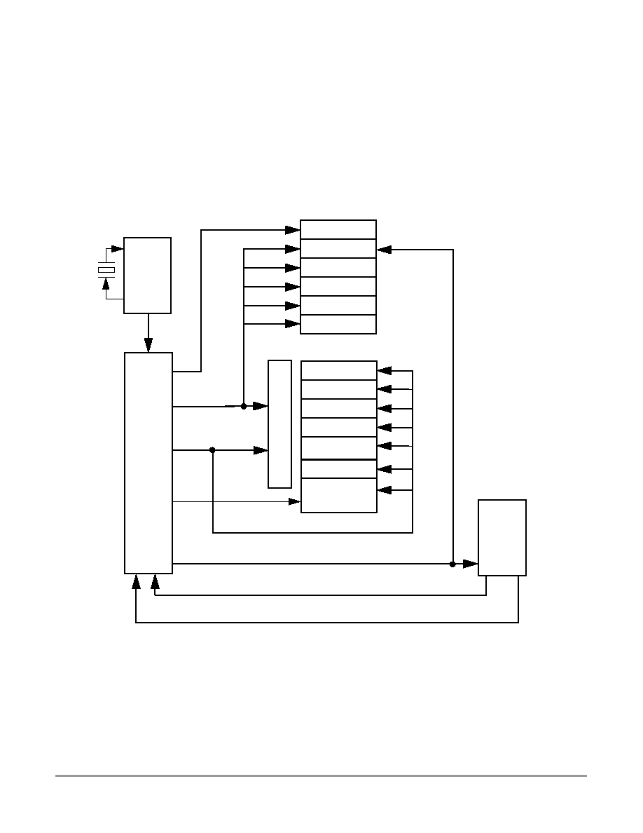
77
Freescale Semiconductor
System on a Chip Guide -- 9S12UF32DGV1/D V01.05
Section 3 System Clock Description
The clock is generated by the USB20PHY analog sub-block in the USB20D6E2F module.The Clock and
Reset Generator distributes the internal clock signals for the core and all peripheral modules.
Figure
3-1
shows the clock connections from the CRG_U to all modules. Consult the CRG_U Block Guide for
details on clock generation.
.
Figure 3-1 Clock Connections
1
NOTES
:
1. UTMI clock and IQUE clock are fixed 30MHz and 60MHz respectively only when PHY (instead of OSC) is selected as the
clock source. See CRG_U Block Guide for details.
CRG_U
IP bus clock
core clock
oscillator clock
IQUE
MSHC
SDHC
SMHC
USB2.0
CFHC
ATA5HC
USB2.0
PHY
30MHz Clock for UTMI Interface
IQUE Clock*
60MHz Clock
EXTAL clock
Digital
EXTAL
XTAL
OSC
IP Bus Interface
UTMI Clock*
TIM
SCI
PIM
SMRAM3P5K2E
Flash
S12_CORE
12MHz

System on a Chip Guide -- 9S12UF32DGV1/D V01.05
78
Freescale Semiconductor
Section 4 Modes of Operation
4.1 Overview
Eight possible modes determine the operating configuration of the MC9S12UF32. Each mode has an
associated default memory map and external bus configuration. In addition each operating mode, with the
exception of Special Peripheral Mode (SPM), can be configured for low power operation by entering one
of two low power sub-modes. The device is also equipped with security features which restrict certain
modes of operation and limit access to internal memory. More detailed information on the various
operating modes, and their configurations can be found in the HCS12 V1.5 Core User Guide.
4.2 Modes of Operation
There are two basic categories of operating modes:
1.
Normal modes: Some registers and bits are protected against accidental changes.
2.
Special modes: Allow greater access to protected control registers and bits for special purposes such
as testing.
In all Normal and Special modes a system development and debug feature, background debug mode
(BDM), is available. In special single-chip mode, BDM is active immediately after reset.
The operating mode out of reset is determined by the states of the MODC, MODB, and MODA pins during
reset (
Table 4-1
). The MODC, MODB, and MODA bits in the MODE register show the current operating
mode and provide limited mode switching during operation. The states of the MODC, MODB, and MODA
pins are latched into these bits on the rising edge of the reset signal. When resetting into all modes except
SPM, the ESTR bit in the EBICTL register is set to one, configuring the ECLK as a bus control signal, to
assure that the reset vector can be fetched even if it located in an external slow memory device.
The following sections discuss the default bus setup and describe which aspects of the bus can be changed
after reset on a per mode basis.
Table 4-1 Mode Selection
BKGD =
MODC
PE6 =
MODB
PE5 =
MODA
Mode Description
0
0
0
Special Single Chip, BDM allowed and ACTIVE. BDM is allowed in all
other modes but a serial command is required to make BDM active.
0
0
1
Emulation Expanded Narrow, BDM allowed
0
1
0
Special Test (Expanded Wide), BDM allowed
0
1
1
Emulation Expanded Wide, BDM allowed
1
0
0
Normal Single Chip, BDM allowed
1
0
1
Normal Expanded Narrow, BDM allowed
1
1
0
Special Peripheral; BDM allowed but bus operations would cause bus
conflicts (must not be used)
1
1
1
Normal Expanded Wide, BDM allowed

79
Freescale Semiconductor
System on a Chip Guide -- 9S12UF32DGV1/D V01.05
4.2.1 Normal Operating Modes
These modes provide three operating configurations: Normal Single-Chip Mode, Normal Expanded Wide
Mode, and Normal Expanded Narrow Mode. Background debug (BDM) is available in all three normal
modes, but must first be enabled for some operations by means of a BDM background command, then
activated.
4.2.1.1 Normal Single-Chip Mode
There is no external expansion bus in this mode. Ports A and B are general purpose I/O pins, initially
configured as high-impedance inputs with their internal pull-ups disabled. Port pins PE[7:2] are general
purpose I/O pins, and port pins PE[1:0] are available as general purpose input only pins. All of Port E pins
are initially configured as high-impedance inputs with internal pull-ups enabled.
The pins associated with Port E bits 6, 5, 3, and 2 cannot be configured for their alternate functions IPIPE1,
IPIPE0, LSTRB, and R/W while the MCU is in normal single chip mode. In normal single chip mode, the
associated control bits PIPOE, LSTRE, and RDWE are reset to zero, and writing a one to them in this mode
does not change the operation of the associated Port E pins.
In normal single chip mode, the MODE register is writable one time. This allows a user program to change
the bus mode to special single chip or normal expanded wide or normal expanded narrow modes and/or
turn on visibility of internal accesses.
Port E, bit 4 can be configured for a free-running ECLK output by clearing NECLK=0. Typically the only
use for an ECLK output while the MCU is in normal single chip mode would be to get a constant speed
clock for use in the external application system.
4.2.1.2 Normal Expanded Wide Mode
In normal expanded wide mode, Ports A and B are configured as a 16-bit multiplexed address and data bus
and Port PE4 is configured as the ECLK output signal. These signals allow external memory and
peripheral devices to be interfaced to the MCU.
Port E pins other than PE4/ECLK are configured as general purpose I/O pins (initially high-impedance
inputs with internal pull-up resistors enabled). Control bits PIPOE, NECLK, LSTRE, and RDWE in the
PEAR register can be used to configure Port E pins to act as bus control outputs instead of general purpose
I/O pins.
It is possible to enable the pipe status signals on Port E bits 6 and 5 by setting the PIPOE bit in the PEAR
register, but it would be unusual to do so in this mode. Development systems where pipe status signals are
monitored would typically use the special variation of this mode.
The Port E bit 2 pin can be re-configured as the R/W bus control signal by writing "1" to the RDWE bit
in the PEAR register. If the expanded system includes external devices that can be written, such as RAM,
the RDWE bit would need to be set before any attempt to write to an external location. If there are no
writable resources in the external system, PE2 can be left as a general purpose I/O pin.

System on a Chip Guide -- 9S12UF32DGV1/D V01.05
80
Freescale Semiconductor
The Port E bit 3 pin can be re-configured as the LSTRB bus control signal by writing "1" to the LSTRE
bit in the PEAR register. The default condition of this pin is a general purpose input because the LSTRB
function is not needed in all expanded wide applications.
The Port E bit 4 pin is initially configured as ECLK output with stretch. The ECLK output function
depends upon the settings of the NECLK bit in the PEAR register, the IVIS bit in the MODE register and
the ESTR bit in the EBICTL register. The ECLK is available for use in external select decode logic or as
a constant speed clock for use in the external application system.
4.2.1.3 Normal Expanded Narrow Mode
The normal expanded narrow mode is used for lower cost production systems that use 8-bit wide external
EPROMs or RAMs. Such systems take extra bus cycles to access 16-bit locations but this may be preferred
over the extra cost of additional external memory devices.
Ports A and B are configured as a 16-bit address bus and Port A is multiplexed with data. Internal visibility
is not available in this mode because the internal cycles would need to be split into two 8-bit cycles.
Since the PEAR register can only be written one time in this mode, use care to set all bits to the desired
states during the single allowed write.
The PE3/LSTRB pin is always a general purpose I/O pin in normal expanded narrow mode. Although it
is possible to write the LSTRE bit in the PEAR register to "1" in this mode, the state of LSTRE is
overridden and Port E bit 3 cannot be re-configured as the LSTRB output.
It is possible to enable the pipe status signals on Port E bits 6 and 5 by setting the PIPOE bit in the PEAR
register, but it would be unusual to do so in this mode. LSTRB would also be needed to fully understand
system activity. Development systems where pipe status signals are monitored would typically use special
expanded wide mode or occasionally special expanded narrow mode.
The PE4/ECLK pin is initially configured as ECLK output with stretch. The ECLK output function
depends upon the settings of the NECLK bit in the PEAR register, the IVIS bit in the MODE register and
the ESTR bit in the EBICTL register. In normal expanded narrow mode, the ECLK is available for use in
external select decode logic or as a constant speed clock for use in the external application system.
The PE2/R/W pin is initially configured as a general purpose input with a pull-up but this pin can be
re-configured as the R/W bus control signal by writing "1" to the RDWE bit in the PEAR register. If the
expanded narrow system includes external devices that can be written such as RAM, the RDWE bit would
need to be set before any attempt to write to an external location. If there are no writable resources in the
external system, PE2 can be left as a general purpose I/O pin.
4.2.1.4 Emulation Expanded Wide Mode
In expanded wide modes, Ports A and B are configured as a 16-bit multiplexed address and data bus and
Port E provides bus control and status signals. These signals allow external memory and peripheral devices
to be interfaced to the MCU. These signals can also be used by a logic analyzer to monitor the progress of
application programs.
The bus control related pins in Port E (PE7/NOACC, PE6/MODB/IPIPE1, PE5/MODA/IPIPE0,
PE4/ECLK, PE3/LSTRB/TAGLO, and PE2/R/W) are all configured to serve their bus control output

81
Freescale Semiconductor
System on a Chip Guide -- 9S12UF32DGV1/D V01.05
functions rather than general purpose I/O. Writes to the bus control enable bits in the PEAR register in
special mode are restricted.
4.2.1.5 Emulation Expanded Narrow Mode
Expanded narrow modes are intended to allow connection of single 8-bit external memory devices for
lower cost systems that do not need the performance of a full 16-bit external data bus. Accesses to internal
resources that have been mapped external (i.e. PORTA, PORTB, DDRA, DDRB, PORTE, DDRE, PEAR,
PUCR, RDRIV) will be accessed with a 16-bit data bus on Ports A and B. Accesses of 16-bit external
words to addresses which are normally mapped external will be broken into two separate 8-bit accesses
using Port A as an 8-bit data bus. Internal operations continue to use full 16-bit data paths. They are only
visible externally as 16-bit information if the IVIS bit is set to one in the MODE register.
Ports A and B are configured as multiplexed address and data output ports. During external accesses,
address A15, data D15 and D7 are associated with PA7, address A0 is associated with PB0 and data D8
and D0 are associated with PA0. During internal visible accesses and accesses to internal resources that
have been mapped external, address A15 and data D15 is associated with PA7 and address A0 and data
D0 is associated with PB0.
The bus control related pins in Port E (PE7/NOACC, PE6/MODB/IPIPE1, PE5/MODA/IPIPE0,
PE4/ECLK, PE3/LSTRB/TAGLO, and PE2/R/W) are all configured to serve their bus control output
functions rather than general purpose I/O. Notice that writes to the bus control enable bits in the PEAR
register in special mode are restricted.
The main difference between special modes and normal modes is that some of the bus control and system
control signals cannot be written in special modes.
4.2.2 Special Operating Modes
There are a total of three special operating modes: Special Single-Chip, Special Test, and Special
Peripheral modes. These operating modes are commonly used in factory testing and system development.
Two of the special operating modes correspond to normal operating modes.
4.2.2.1 Special Single-Chip Mode
When the MCU is reset in this mode, the background debug mode is enabled and active. The MCU does
not fetch the reset vector and execute application code as it would in other modes. Instead, the active
background mode is in control of CPU execution and BDM firmware is waiting for additional serial
commands through the BKGD pin. When a serial command instructs the MCU to return to normal
execution, the system will be configured as described below unless the reset states of internal control
registers have been changed through background commands after the MCU was reset.
There is no external expansion bus after reset in this mode. Ports A and B are initially simple bidirectional
I/O pins that are configured as high-impedance inputs with internal pull-ups disabled; however, writing to
the mode select bits in the MODE register (which is allowed in special modes) can change this after reset.
All of the Port E pins (except PE4/ECLK) are initially configured as general purpose high-impedance
inputs with pull-ups enabled. PE4/ECLK is configured as the ECLK output in this mode.

System on a Chip Guide -- 9S12UF32DGV1/D V01.05
82
Freescale Semiconductor
The pins associated with Port E bits 6, 5, 3, and 2 cannot be configured for their alternate functions IPIPE1,
IPIPE0, LSTRB, and R/W while the MCU is in single chip modes In single chip modes, the associated
control bits PIPOE, LSTRE and RDWE are reset to zero. Writing the opposite value into these bits in
single chip mode does not change the operation of the associated Port E pins.
Port E, bit 4 can be configured for a free-running ECLK output by clearing NECLK=0. Typically the only
use for an ECLK output while the MCU is in single chip modes would be to get a constant speed clock for
use in the external application system.
4.2.2.2 Special Test Mode
In expanded wide modes, Ports A and B are configured as a 16-bit multiplexed address and data bus and
Port E provides bus control and status signals. In special test mode, the write protection of many control
bits is lifted so that they can be thoroughly tested without needing to go through reset.
4.2.2.3 Special Peripheral Mode
This mode is intended for Motorola factory testing of the MCU. In this mode, the CPU is inactive and an
external (tester) bus master drives address, data and bus control signals in through Ports A, B and E. In
effect, the whole MCU acts as if it was a peripheral under control of an external CPU. This allows faster
testing of on-chip memory and peripherals than previous testing methods. Since the mode control register
is not accessible in peripheral mode, the only way to change to another mode is to reset the MCU into a
different mode. Background debugging should not be used while the MCU is in special peripheral mode
as internal bus conflicts between BDM and the external master can cause improper operation of both
functions.
4.3 Internal Visibility
Internal visibility is available when the MCU is operating in expanded wide modes or special test modes.
It is not available in single-chip, peripheral or normal expanded narrow modes. Internal visibility is
enabled by setting the IVIS bit in the MODE register.
If an internal access is made while the ECLK, R/W, and LSTRB are configured as bus control outputs and
internal visibility is off (IVIS=0), ECLK will remain low for the cycle, R/W will remain high, and address,
data and the LSTRB pins will remain at their previous state.
When internal visibility is enabled (IVIS=1), certain internal cycles will be blocked from going external.
During cycles when the BDM is selected, R/W will remain high, data will maintain its previous state, and
address and LSTRB pins will be updated with the internal value. During CPU no access cycles when the
BDM is not driving, R/W will remain high, and address, data and the LSTRB pins will remain at their
previous state.
4.4 Security
The device will make available a security feature preventing the unauthorized read and write of the
memory contents. This feature allows:

83
Freescale Semiconductor
System on a Chip Guide -- 9S12UF32DGV1/D V01.05
∑
Protection of the contents of FLASH,
∑
Operation in single-chip mode,
∑
Operation from external memory with internal FLASH disabled.
The user must be reminded that part of the security must lie with the user's code. An extreme example
would be user's code that dumps the contents of the internal program. This code would defeat the purpose
of security. At the same time the user may also wish to put a back door in the user's program. An example
of this is the user downloads a key through the SCI which allows access to a programming routine that
updates parameters stored in FLASH. Please refer to the HCS12 Core User Guide for more information
about security.
4.4.1 Securing the Microcontroller
Once the user has programmed the FLASH, the part can be secured by programming the security bits
located in the FLASH module. These non-volatile bits will keep the part secured through resetting the part
and through powering down the part.
The security byte resides in a portion of the Flash array.
Check the Flash Block Guide for more details on the security configuration.
4.4.2 Operation of the Secured Microcontroller
4.4.2.1 Normal Single Chip Mode
This will be the most common usage of the secured part. Everything will appear the same as if the part was
not secured with the exception of BDM operation. The BDM operation will be blocked.
4.4.2.2 Executing from External Memory
The user may wish to execute from external space with a secured microcontroller. This is accomplished
by resetting directly into expanded mode. The internal FLASH will be disabled. BDM operations will be
blocked.
4.4.3 Unsecuring the Microcontroller
There are two methods for unsecuring the Microcontroller. If the contents of the flash are known then the
microcontroller can be unsecured using the backdoor key access feature. The other unsecuring method is
to fully erase the FLASH.
4.4.3.1 Unsecuring the Microcontroller (backdoor key access)
In normal modes, either SINGLE CHIP or EXPANDED, the microcontroller may only be unsecured by
using the backdoor key access feature. This requires knowledge of the contents of the backdoor keys,
which must be written to the Flash memory space at the appropriate addresses, in the correct order. In
addition, in SINGLE CHIP mode the user code stored in the Flash must have a method of receiving the
backdoor key from an external stimulus. This external stimulus would typically be through one of the

System on a Chip Guide -- 9S12UF32DGV1/D V01.05
84
Freescale Semiconductor
on-chip serial ports. After the backdoor sequence has been correctly matched, the microcontroller will be
unsecured, and all Flash commands will be enabled and the Flash security byte can be programmed to the
unsecure state, if desired.
Please note that if the system goes through a reset condition prior to successful configuration of unsecured
mode the system will reset back into secured mode operation.
4.4.3.2 Unsecuring the Microcontroller (full FLASH erase)
In order to unsecure the microcontroller, the internal FLASH must be erased. This can be done through an
external program in expanded mode.
Once the user has erased the FLASH, the part can be reset into special single chip mode This invokes a
program that verifies the erasure of the internal FLASH. Once this program completes, the user can erase
and program the FLASH security bits to the unsecured state. This is generally done through the BDM, but
the user could also change to expanded mode (by writing the mode bits through the BDM) and jumping to
an external program (again through BDM commands). Note that if the part goes through a reset before the
security bits are reprogrammed to the unsecure state, the part will be secured again.
4.5 Low Power Modes
There are two low power modes available on the MC9S12UF32: Stop and Wait
Please see
Table A-8
for device operating characteristics in Stop and Wait modes. Consult the CRG_U
Block Guide and the respective Block Guide for information on the module behavior in Stop and Wait
Mode.
4.5.1 Stop
Executing the CPU STOP instruction stops all clocks and the oscillator, thus putting the chip in fully static
mode. Wake up from this mode can be done via reset or external interrupts.
4.5.2 Wait
This mode is entered by executing the CPU WAI instruction. In this mode, the CPU will not execute
instructions. The internal CPU signals (address and data bus) will be fully static. All peripherals stay
active. So, for example, data can still be transferred from ATA5HC to USB via IQUE. For further power
consumption, the peripherals can individually turn off their local clocks.
4.5.3 Run
Although this is not a low power mode, unused peripheral modules should not be enabled in order to save
power.

85
Freescale Semiconductor
System on a Chip Guide -- 9S12UF32DGV1/D V01.05
Section 5 Resets and Interrupts
5.1 Overview
Consult the Exception Processing section of the HCS12 Core User Guide for information on resets and
interrupts. Both local masking and CCR masking are included as listed in
Table 5-1
. System resets can
be generated through external control of the RESET pin, through the clock and reset generator module
CRG_U. Refer to the CRG_U User Guide for detailed information on reset generation.
5.2 Vectors
5.2.1 Vector Table
Table 5-1
lists interrupt sources and vectors in default order of priority.
Table 5-1 Interrupt Vector Locations
Vector Address
Interrupt Source
CCR
Mask
Local Enable
HPRIO Value
to Elevate
$FFFE, $FFFF
Reset
None
None
≠
$FFFC, $FFFD
Reserved
None
Reserved
≠
$FFFA, $FFFB
COP failure reset
None
COP rate select
≠
$FFF8, $FFF9
Unimplemented instruction trap
None
None
≠
$FFF6, $FFF7
SWI
None
None
≠
$FFF4, $FFF5
XIRQ
X-Bit
None
≠
$FFF2, $FFF3
IRQ
I-Bit
INTCR (IRQEN)
$F2
$FFF0, $FFF1
Real Time Interrupt
I-Bit
CRGINT (RTIE)
$F0
$FFEE, $FFEF
Timer channel 0
I-Bit
TIE (C0I)
$EE
$FFEC, $FFED
Timer channel 1
I-Bit
TIE (C1I)
$EC
$FFEA, $FFEB
Timer channel 2
I-Bit
TIE (C2I)
$EA
$FFE8, $FFE9
Timer channel 3
I-Bit
TIE (C3I)
$E8
$FFE6, $FFE7
Timer channel 4
I-Bit
TIE (C4I)
$E6
$FFE4, $FFE5
Timer channel 5
I-Bit
TIE (C5I)
$E4
$FFE2, $FFE3
Timer channel 6
I-Bit
TIE (C6I)
$E2
$FFE0, $FFE1
Timer channel 7
I-Bit
TIE (C7I)
$E0
$FFDE, $FFDF
Timer overflow
I-Bit
TSCR2 (TOI)
$DE
$FFDC, $FFDD
Pulse accumulator A overflow
I-Bit
PACTL (PAOVI)
$DC
$FFDA, $FFDB
Pulse accumulator input edge
I-Bit
PACTL (PAI)
$DA
$FFD8, $FFD9
Reserved
-
Reserved
$D8
$FFD6, $FFD7
SCI
I-Bit
SCICR2
(TIE, TCIE, RIE, ILIE)
$D6
$FFD4, $FFD5
USB status change
I-Bit
UIMR(USSCIE, URSCIE)
$D4
$FFD2, $FFD3
USB Setup command related
I-Bit
UIMR (SETOVRIE, SETUP)
$D2
$FFD0, $FFD1
USB set endpoint configuration register
request
I-Bit
UCCSR(SETECRIE)
$D0
$FFCE, $FFCF
USB Endpoint 0 IN
I-Bit
UEPCSR0 (TCIE)
$CE

System on a Chip Guide -- 9S12UF32DGV1/D V01.05
86
Freescale Semiconductor
$FFCC, $FFCD
USB Endpoint 0 OUT
I-Bit
UEPCSR1 (TCIE)
$CC
$FFCA, $FFCB
USB Endpoint 2
I-Bit
UEPCSR2 (TCIE)
$CA
$FFC8, $FFC9
USB Endpoint 3
I-Bit
UEPCSR3 (TCIE)
$C8
$FFC6, $FFC7
CRG PLL Lock
I-Bit
PLLCR (LOCKIE)
$C6
$FFC4, $FFC5
USB Endpoint 4
I-Bit
UEPCSR4A (TCIE),
UEPCSR4B (SPKTIE,
TERRIE)
$C4
$FFC2, $FFC3
USB Endpoint 5
I-Bit
UEPCSR5A (TCIE),
UEPCSR5B (SPKTIE,
TERRIE)
$C2
$FFC0, $FFC1
USB Endpoint 6
I-Bit
UEPCSR6 (TCIE)
$C0
$FFBE, $FFBF
USB Start of Frame
I-Bit
UIMR (SOFIE)
$BE
$FFBC, $FFBD
Reserved
I-Bit
Reserved
$BC
$FFBA, $FFBB
Reserved
I-Bit
Reserved
$BA
$FFB8, $FFB9
FLASH
I-Bit
FCTL(CCIE, CBEIE)
$B8
$FFB6, $FFB7
IQUE Channel 1 Full
I-Bit
QC1CR (Q1FIE)
$B6
$FFB4, $FFB5
IQUE Channel 1 Empty
I-Bit
QC1CR (Q1EIE)
$B4
$FFB2, $FFB3
IQUE Channel 1 Valid
I-Bit
QC1CR (Q1VIE)
$B2
$FFB0, $FFB1
IQUE Channel 2 Full
I-Bit
QC2CR (Q2FIE)
$B0
$FFAE, $FFAF
IQUE Channel 2 Empty
I-Bit
QC2CR (Q2EIE)
$AE
$FFAC, $FFAD
IQUE Channel 2 Valid
I-Bit
QC2CR (Q2VIE)
$AC
$FFAA, $FFAB
IQUE Channel 3 Full
I-Bit
QC3CR (Q3FIE)
$AA
$FFA8, $FFA9
IQUE Channel 3 Empty
I-Bit
QC3CR (Q3EIE)
$A8
$FFA6, $FFA7
IQUE Channel 3 Valid
I-Bit
QC3CR (Q3VIE)
$A6
$FFA4, $FFA5
IQUE Channel 4 Full
I-Bit
QC4CR (Q4FIE)
$A4
$FFA2, $FFA3
IQUE Channel 4 Empty
I-Bit
QC4CR (Q4EIE)
$A2
$FFA0, $FFA1
IQUE Channel 4 Valid
I-Bit
QC4CR (Q4VIE)
$A0
$FF9E, $FF9F
IQUE Channel 1/2 Double Buffer Full
I-Bit
QC12DCR (DVFIE)
$9E
$FF9C, $FF9D
IQUE Channel 1/2 Double Buffer Empty
I-Bit
QC12DCR (DVEIE)
$9C
$FF9A, $FF9B
IQUE Channel 1/2 Double Buffer
Transfer Complete
I-Bit
QC12DCR (DVTIE)
$9A
$FF98, $FF99
IQUE Channel 3/4 Double Buffer Full
I-Bit
QC34DCR (DVFIE)
$98
$FF96, $FF97
IQUE Channel 3/4 Double Buffer Empty
I-Bit
QC34DCR (DVEIE)
$96
$FF94, $FF95
IQUE Channel 3/4 Double Buffer
Transfer Complete
I-Bit
QC34DCR (DVTIE)
$94
$FF92, $FF93
Reserved
-
Reserved
$92
$FF90, $FF91
Reserved
-
Reserved
$90
$FF8E, $FF8F
ATA5 Host Controller
I-Bit
HCFG (IE)
$8E
$FF8C, $FF8D
CF Host Controller (SFT)
I-Bit
CFSCR1
$8C
$FF8A, $FF8B
CF Host Controller (IREQ)
I-Bit
CFSCR1
$8A
$FF88, $FF89
MS Host Controller
I-Bit
MSIC (INTE, DTRQIE,
DTCMPIE, FAEEN)
$88
$FF86, $FF87
SD Host Controller
I-Bit
SDINTREN
$86
$FF84, $FF85
SM Host Controller Error
I-Bit
SMIMR(INTEN)
$84
$FF82, $FF83
SM Host Controller Status
I-Bit
SMIMR(INTEN)
$82
$FF80, $FF81
Reserved
-
Reserved
$80

87
Freescale Semiconductor
System on a Chip Guide -- 9S12UF32DGV1/D V01.05
5.3 Resets
Resets are a subset of the interrupts featured in
Table 5-1
. The different sources capable of generating a
system reset are summarized in
Table 5-2
.
5.3.1 Reset Summary Table
5.3.2 Effects of Reset
When a reset occurs, MCU registers and control bits are changed to known start-up states. Refer to the
respective module Block Guides for register reset states. Refer to the HCS12 Core User Guides for mode
dependent pin configuration of port A, B and E out of reset.
Refer to the PIM Block Guide for reset configurations of all peripheral module ports.
Refer to for location of the memories depending on the operating mode after reset.
The RAM array is not automatically initialized out of reset.
Table 5-2 Reset Summary
Reset
Priority
Source
Vector
Power-on Reset
1
CRG Module
$FFFE, $FFFF
External Reset
1
RESET pin
$FFFE, $FFFF
COP Watchdog Reset
2
CRG Module
$FFFA, $FFFB

System on a Chip Guide -- 9S12UF32DGV1/D V01.05
88
Freescale Semiconductor
Section 6 HCS12 Core Block Description
6.1 CPU12 Block Description
Consult the CPU12 Reference Manual for information about the Central Processing Unit.When the
CPU12 Reference Manual refers to cycles, this is equivalent to Bus Clock periods. So 1 cycle is equivalent
to 1 Bus Clock period.
6.2 HCS12 Background Debug Module (BDM) Block Description
Consult the HCS12 BDM Block Guide for information about the Background Debug Module.When the
BDM Block Guide refers to alternate clock, this is equivalent to Oscillator Clock.
6.3 HCS12 Breakpoint (BKP) Block Description
Consult the HCS12 BKP Block Guide for information about the Breakpoint module.
6.4 HCS12 Interrupt (INT) Block Description
Consult the HCS12 INT Block Guide for information about the Interrupt module.
6.5 HCS12 Multiplexed External Bus Interface (MEBI) Block
Description
Consult the HCS12 MEBI Block Guide for information about the Multiplexed External Bus Interface
module.
6.6 HCS12 Module Mapping Control (MMC) Block Description
Consult the HCS12 MMC Block Guide for information about the Module Mapping Control module.
Section 7 ATA5 Host Controller (ATA5HC) Block
Description
Consult the ATA5HC Block Guide for information about the ATA5 host controller module.

89
Freescale Semiconductor
System on a Chip Guide -- 9S12UF32DGV1/D V01.05
7.1 Device-specific information
The ATA5HC is part of the IQUE bus domain.
The register spaces for the ATA5HC is located at addresses $01C0-$01FF.
Section 8 Compact Flash Host Controller (CFHC) Block
Description
Consult the CFHC Block Guide for information about the Compact Flash host controller module.
8.1 Device-specific information
The CFHC is part of the IQUE bus domain.
The register spaces for the CFHC is located at addresses $0280-$029F.
The module inputs CD1, CD2, CVCC, SPKR, STSCHG, VS1, VS2 and the module output CRESET are
not used in MC9S12UF32 (i.e. not connected to chip I/O pins) and are internally tied to constant values.
User can use GPIO pins for these CF card interface if necessary.
Section 9 Clock Reset Generator (CRG_U) Block
Description
Consult the CRG_U Block Guide for information about the Clock and Reset Generator module.
9.1 Device-specific information
The CRG_U is part of the IPBus domain.
The register space for the CRG_U is located at addresses $0034-$003F.
Section 10 Flash EEPROM 32K (FTS32K) Block Description
Consult the FTS32K Block Guide for information about the 32K Flash EEPROM module.

System on a Chip Guide -- 9S12UF32DGV1/D V01.05
90
Freescale Semiconductor
10.1 Device-specific information
The FTS32K is part of the HCS12 Bus domain.
The register spaces for the FTS32K is located at addresses $0100-$010F.
The memory spaces for the FTS32K is located at addresses $8000-$FFFF upon reset. Addresses
$4000-$7FFF also map to the same flash array at $8000-$BFFF.
Section 11 Integrated Queue Controller (IQUE) Block
Description
Consult the IQUE Block Guide for information about the Integrated Queue Controller module.
11.1 Device-specific information
The IQUE is part of the IQUE Bus domain, with the QRAM interface in HCS12 Bus domain.
The register spaces for the IQUE is located at addresses $0200-$023F.
The memory spaces for the IQUE is located at addresses $0000-$07FF ($0600-$07FF is reserved) upon
reset and is mappable to any 2k-byte boundary.
The Channel Request Mapping for the IQUE module on the UF32 is shown in
Table 11-1
.
Table 11-1 Queue Channel n Request Mapping
QnREQ
Peripheral Function
Direction (Rx/Tx)
0000
USB20D6E2F
Rx
0001
USB20D6E2F
Tx
0010
ATA5HC
Rx
0011
ATA5HC
Tx
0100
CFHC
Rx
0101
CFHC
Tx
0110
MSHC
Rx
0111
MSHC
Tx
1000
SDHC
Rx
1001
SDHC
Tx
1010
SMHC
Rx
1011
SMHC
Tx

91
Freescale Semiconductor
System on a Chip Guide -- 9S12UF32DGV1/D V01.05
Section 12 Memorystick Host Controller (MSHC) Block
Description
Consult the MSHC Block Guide for information about the Memorystick host controller module.
12.1 Device-specific information
The MSHC is part of the IQUE bus domain.
The register spaces for the MSHC is located at addresses $02A0-$02AF.
Section 13 Oscillator (OSC) Block Description
Consult the OSC Block Guide for information about the Oscillator module.
13.1 Device-specific information
The power of the OSC module, XTAL and EXTAL pins are supplied directly by internal voltage regulator
(instead of VDDPLL/VSSPLL in the OSC Block Guide). The ground is connected to VSSA.
Colpitts oscillator and clock monitor of the OSC module are not available in this chip.
Only Pierce oscillator/external clock circuitry is allowed. The XCLKS input of the OSC module is tied
internally.
Figure 13-1 Pierce Oscillator Connections
Section 14 Port Integration Module (PIM) Block Description
Consult the PIM_9UF32 Block Guide for information about the Port Integration Module.
MCU
EXTAL
XTAL
R
B
VSSA
12MHz crystal or
ceramic resonator
C
2
C
1

System on a Chip Guide -- 9S12UF32DGV1/D V01.05
92
Freescale Semiconductor
14.1 Device-specific information
The PIM is part of the IPBus domain.
The MODRR register within the PIM allows for pin mapping for the 100LQFP package and for the 64
LQFP package.
Section 15 Serial Communication Interface (SCI) Block
Description
Consult the SCI Block Guide for information about the Serial Communication Interface module.
15.1 Device-specific information
The SCI is part of the IPBus domain.
The register spaces for the timer is located at addresses $00C8-$00CF.
Section 16 Secured Digital Host Controller (SDHC) Block
Description
Consult the SDHC Block Guide for information about the Secured Digital host controller module.
16.1 Device-specific information
The SDHC is part of the IQUE bus domain.
The register spaces for the SDHC is located at addresses $02C0-$02DF.
Section 17 Smartmedia Host Controller (SMHC) Block
Description
Consult the SMHC Block Guide for information about the Smartmedia host controller module.

93
Freescale Semiconductor
System on a Chip Guide -- 9S12UF32DGV1/D V01.05
17.1 Device-specific information
The SMHC is part of the IQUE bus domain.
The register spaces for the SMHC is located at addresses $02B0-$02BF.
Section 18 Smartmedia RAM (SMRAM) Block Description
Consult the SMRAM Block Guide for information about the Smartmedia RAM module.
18.1 Device-specific information
The SMRAM is part of the HCS12 Bus domain.
The register space for the SMRAM is located at addresses $011C-$011F.
The memory space for the SMRAM is located at addresses $0800-$1FFF upon reset and is mappable to
any 8k-byte boundary.
Section 19 Timer (TIM) Block Description
Consult the TIM_16B8C Block Guide for information about the Timer module.
19.1 Device-specific information
The TIM is part of the IPBus domain.
The register spaces for the timer is located at addresses $0040-$006F.
Section 20 USB2.0 Controller (USB20D6E2F) Block
Description
Consult the USB20D6E2F Block Guide for information about the USB2.0 Device Controller module.
20.1 Device-specific information
The USB 2.0 Serial Interface Engine (USB20SIE) is part of the IQUE bus domain.

System on a Chip Guide -- 9S12UF32DGV1/D V01.05
94
Freescale Semiconductor
The USB 2.0 Physical Layer (USB20PHY) is an analog plus high speed digital hard block.
The register spaces for the USB20D6E2F is located at addresses $0300-$03FF.
Section 21 Voltage Regulator (VREG_U) Block Description
Consult the VREG_U Block Guide for information about the voltage regulator.
21.1 Device-specific information
The VREG_U is part of the IPBus domain.
In 64-pin LQFP package version, the regulator enable pin (VREGEN) is not available externally and is
connected internally to VDDR.
Section 22 Schematic and PCB Layout Design
Recommendations
This section provides recommendations for schematic and PCB layout design for implementing an USB
interface with the MC9S12UF32 microcontroller unit (MCU).
22.1 Schematic Design with the MC9S12UF32 and a USB interface
Figure 22-1
is a schematic of a MC9S12UF32 64-pin package minimum system implementation
configured in single-chip mode and utilizing the internal voltage regulator. Same connections can be used
with MC9S12UF32 100-pin package. The schematic provides a reference for the following
MC9S12UF32 design items:
∑
Operation mode
∑
Clocks
∑
Power
∑
USB connector (CON1)
∑
Background debug connector (CON2)
To configure the MC9S12UF32 in normal single-chip mode, the MODC, MODB, and MODA pins should
be configured as documented in the device overview chapter of this book.

95
Freescale Semiconductor
System on a Chip Guide -- 9S12UF32DGV1/D V01.05
Figure 22-1 Sample schematic with 64-pin LQFP MC9S12UF32
22.1.1 Power Supply Notes
A 5V power is required.
Figure 22-1
shows an example of bus-powered USB device. Special
considerations are needed in the choice of capacitors and other power consumptions of the board in order
to fulfil the USB current requirement. Alternatively, the board can be designed for self-powered USB
device.
22.1.2 Clocking Notes
For proper operation of USB and storage interface of the MC9S12UF32, a 12-MHz crystal is required to
provide the clock input to the integrated USB PHY. The crystal must connect to the MC9S12UF32 in a
Pierce configuration by the XTAL and EXTAL pins as shown.
BKGD
RESETB
5V
1
2
3
4
5
6
7
8
9
10
11
12
13
14
15
16
48
47
46
45
44
43
42
41
40
39
38
37
36
35
34
33
17
18
19
20
21
22
23
24
25
26
27
28
29
30
31
32
64
63
62
61
60
59
58
57
56
55
54
53
52
51
50
49
MC9S12UF32
64 LQFP
3V3
REF3V
3V3
EXTAL
XTAL
X1
C7 (22pF)
C8 (22pF)
R5
(1M
)
(12MHz)
5V
DMH
DMF
DPF
DPH
L1
R21 (10
)
R1 (33
)
R2 (33
)
R22 (10
)
VDD
GND
D-
D+
1
2
3
4
5V
R10 (3.3K
)
BKGD
RESETB
5V
1
2
3
4
CON2
CON1
(USB Input)
C5 (100nF)
R3 (510
)
R4 (1.5K
)
5V
C1 (4.7uF)
C3(100nF)
C2 (4.7uF)
C4 (100nF)
C6 (5nF)
REF3V
3V3
Q1
MMBF0201N
EXTAL
XTAL
DMH
DMF
DPH
DPF
RREF
VSSA1
DMH
DMF
DPH
DPF
VDDA
RPU
VSSA
EXTAL
XTAL
VDDX
VSSX
REF3V
VDDR
VSSR
RESET
TEST
BKGD
MODB M
O
D
A
VDD3X
VSS3X

System on a Chip Guide -- 9S12UF32DGV1/D V01.05
96
Freescale Semiconductor
22.2 PCB Design Recommendation
The PCB must be carefully laid out to ensure proper operations of the voltage regulator as well as the MCU
itself. The following rules must be observed:
∑
Every supply pair must be decoupled by a ceramic capacitor connected as near as possible to the
corresponding pins.
∑
Central point of the ground star should be the VSSR pin.
∑
Use low ohmic, low inductance connections between VSSR, VSSX, VSS3X, VSSA and VSSA1.
∑
Keep traces of VSSA, EXTAL and XTAL as short as possible and occupied board area for C7, C8
and X1 as small as possible.
∑
Do not place other signals or supplies underneath area occupied by C7, C8 and X1, and the
connection area to the MCU.
∑
Central power input should be fed in at the VDDR/VSSR pins.
Table 22-1 Recommended decoupling capacitor choice
Component
Purpose
Type
Value
C1
decoupling cap
X7R/tantalum
>=100nF
C2
decoupling cap
X7R/tantalum
>=100nF
C3
decoupling cap
ceramic X7R
100nF
C4
decoupling cap
ceramic X7R
100nF
C5
decoupling cap
ceramic X7R
100nF
C6
decoupling cap
choice of C6 cap depends on the
type of NMOS transistor
Q1
NMOS transistor
R1
DMF resistor
impedance matching resistors
depend on board design
R2
DPF resistor
R21
DMH resistor
R22
DMF resistor
R3
RREF resistor
See Voltage Regulator Appendix
R4
RPU resistor
C7
OSC load cap
See crystal manufacturer's
recommendations
C8
OSC load cap
R5
OSC resistor
X1
Quartz

97
Freescale Semiconductor
System on a Chip Guide -- 9S12UF32DGV1/D V01.05
Appendix A Electrical Characteristics
A.1 General
This introduction is intended to give an overview on several common topics like power supply, current
injection etc.
A.1.1 Parameter Classification
The electrical parameters shown in this supplement are guaranteed by various methods. To give the
customer a better understanding the following classification is used and the parameters are tagged
accordingly in the tables where appropriate.
NOTE:
This classification will be added at a later release of the specification
P: Those parameters are guaranteed during production testing on each individual device.
C: Those parameters are achieved by the design characterization by measuring a statistically relevant
sample size across process variations. They are regularly verified by production monitors.
T: Those parameters are achieved by design characterization on a small sample size from typical devices.
All values shown in the typical column are within this category.
D: Those parameters are derived mainly from simulations.
A.1.2 Power Supply
The MC9S12UF32 utilizes several pins to supply power to the I/O ports, the oscillator, USB physical layer
interface as well as the digital core.
The VDDX, VSSX pair supplies the 3.3V/5V I/O pins of ports A, B, R, S, and U.
The VDD3X, VSS3X pair supplies the 3.3V/5V I/O pins of ports J, M, Q, P, and T.
The VDDR, VSSR pair supplies the internal voltage regulator and 5V only I/O pins.
VDD is the output supply pin for the core digital logic, generated by the on-chip regulator.
VDDA, VSSA and VSSA1 are output supply pins for the USB physical layer interface I/O pins, supplied
by the on-chip regulator.
VSS3X and VSSX are connected by anti-parallel diodes for ESD protection.
VSS3X and VSSR are connected by anti-parallel diodes for ESD protection.
VSSA1 and VSSR are connected by anti-parallel diodes for ESD protection.
NOTE:
IDD3 denotes the currents flowing into VDD3X
IDDR denotes the currents flowing into the VDDR
IDDX denotes the current flowing into VDDX

System on a Chip Guide -- 9S12UF32DGV1/D V01.05
98
Freescale Semiconductor
A.1.3 Pins
There are six groups of functional pins.
A.1.3.1 3.3V/5.0V I/O pins on VDDX
Those I/O pins have a nominal level of 3.3V or 5.0V depending on the voltage supplied by VDDX. This
group of pins is comprised of all port I/O pins.The internal structure of all those pins is identical, however
some of the functionality may be disabled.
A.1.3.2 3.3V/5.0V I/O pins on VDD3X
Those I/O pins have a nominal level of 3.3V or 5.0V depending on the voltage supplied by VDD3X. This
group of pins is comprised of all port I/O pins.The internal structure of all those pins is identical, however
some of the functionality may be disabled.
A.1.3.3 5.0V I/O pins
Those I/O pins have a nominal level of 5.0V with power rail connecting to VDDR. This group of pins is
comprised of all port I/O pins.The internal structure of all those pins is identical, however some of the
functionality may be disabled.
A.1.3.4 USB physical layer interface analog pins
Those I/O pins have specific analog function dedicated to the USB PHY interface and are supplied by
internally generated 3.3V VDDA.
A.1.3.5 Oscillator
The pins EXTAL and XTAL dedicated to the oscillator have a nominal 2.5V level. They are supplied by
internal 2.5V regulator.
A.1.3.6 TEST
This pin is used for production testing only and must be tied to VSS in normal application.
A.1.4 Current Injection
Power supply must maintain regulation within operating specified range during instantaneous and
operating maximum current conditions. If positive injection current (V
in
> supply rail voltage) is greater
than supply current of the pin group, the injection current may flow out of supply rail and could result in
external power supply going out of regulation. Insure external supply load will shunt current greater than
maximum injection current. This will be the greatest risk when the MCU is not consuming power; e.g. if
no system clock is present, or if clock rate is very low which would reduce overall power consumption.

99
Freescale Semiconductor
System on a Chip Guide -- 9S12UF32DGV1/D V01.05
A.1.5 Absolute Maximum Ratings
Absolute maximum ratings are stress ratings only. A functional operation under or outside those maxima
is not guaranteed. Stress beyond those limits may affect the reliability or cause permanent damage of the
device.
This device contains circuitry protecting against damage due to high static voltage or electrical fields;
however, it is advised that normal precautions be taken to avoid application of any voltages higher than
maximum-rated voltages to this high-impedance circuit. Reliability of operation is enhanced if unused
inputs are tied to an appropriate logic voltage level (e.g., either V
SSX
or V
DDX
).
A.1.6 ESD Protection and Latch-up Immunity
During the device qualification, ESD stresses were performed for the Human Body Model (HBM) and the
Machine Model (MM).
Table A-1 Absolute Maximum Ratings
Num
Rating
Symbol
Min
Max
Unit
1
I/O, Regulator Voltage
V
DD5
1
NOTES
:
1. This include VDDR, VDDX and VDD3X
-0.3
6.5
V
2
Digital Logic Supply Voltage
2
2. The device contains an internal voltage regulator to generate the logic and analog supply out of the regulator
supply. The absolute maximum ratings apply when the device is powered from an external source.
V
DD
-0.3
3.0
V
3
USB PHY Supply Voltage
2
V
DDA
-0.3
4.0
V
4
Voltage difference VSSX to VSSR and VSSA
VSSX
-0.3
0.3
V
5
Digital I/O Input Voltage
V
IN
-0.3
6.5
V
6
EXTAL, XTAL inputs
V
ILV
-0.3
3.0
V
7
TEST input
V
TEST
-0.3
10.0
V
8
Instantaneous Maximum Current
Single pin limit for all digital I/O pins
3
3. All digital I/O pins are internally clamped to V
SSX
and V
DDX
, V
SS3X
and V
DD3X
, V
SSR
and V
DDR
or V
SSA
and
V
DDA
.
I
D
-25
+25
mA
9
Instantaneous Maximum Current
Single pin limit for EXTAL, XTAL
I
DL
-25
+25
mA
10
Instantaneous Maximum Current
Single pin limit for TEST
4
4. This pin is clamped low to V
SSR
, but not clamped high. This pin must be tied low in applications.
I
DT
-0.25
0
mA
11
Operating Temperature Range (packaged)
T
A
0
70
į
C
12
Operating Temperature Range (junction)
T
J
0
105
į
C
13
Storage Temperature Range
T
stg
≠ 65
155
į
C

System on a Chip Guide -- 9S12UF32DGV1/D V01.05
100
Freescale Semiconductor
A device will be defined as a failure if after exposure to ESD pulses, the device no longer meets the device
specification. Complete DC parametric and functional testing is performed per the applicable device
specification at room temperature followed by hot temperature unless specified otherwise in the device
specification.
A.1.7 Operating Conditions
This chapter describes the operating conditions of the device. Unless otherwise noted those conditions
apply to all the following data.
Table A-2 ESD and Latch-up Test Conditions
Model
Description
Symbol
Value
Unit
Human Body
Series Resistance
R1
1500
Ohm
Storage Capacitance
C
100
pF
Number of Pulse per pin
positive
negative
-
-
1
1
Machine
Series Resistance
R1
0
Ohm
Storage Capacitance
C
200
pF
Number of Pulse per pin
positive
negative
-
-
1
1
Latch-up
Minimum input voltage limit
-2.5
V
Maximum input voltage limit
7.5
V
Table A-3 ESD and Latch-Up Protection Characteristics
Num C
Rating
Symbol
Min
Max
Unit
1
C Human Body Model (HBM)
V
HBM
2000
-
V
2
C Machine Model (MM)
V
MM
200
-
V
3
C
Latch-up Current at T
A
= 70
į
C
positive
negative
I
LAT
+100
-100
-
mA

101
Freescale Semiconductor
System on a Chip Guide -- 9S12UF32DGV1/D V01.05
NOTE:
Instead of specifying ambient temperature all parameters are specified for the more
meaningful silicon junction temperature. For power dissipation calculations refer
to Section A.1.8 Power Dissipation and Thermal Characteristics.
A.1.8 Power Dissipation and Thermal Characteristics
Power dissipation and thermal characteristics are closely related. The user must assure that the maximum
operating junction temperature is not exceeded. The average chip-junction temperature (T
J
) in
į
C can be
obtained from:
The total power dissipation can be calculated from:
Table A-4 Operating Conditions
Rating
Symbol
Min
Typ
Max
Unit
Regulator Supply Voltage
V
DDR
4.25
5.0
5.5
V
VDDX Supply Voltage
V
DDX
3.0
5.0
5.5
V
VDD3X Supply Voltage
V
DD3x
3.0
3.3
5.5
1
NOTES
:
1. REF3V regulator channel cannot be used when VDD3X is not supplied by the regulated supply controlled by
REF3V.
V
Digital Logic Supply Voltage
2
2. The device contains an internal voltage regulator to generate the logic and USB PHY supply out of the VDDR.
The absolute maximum ratings apply when this regulator is disabled and the device is powered from an external
source.
V
DD
2.25
2.5
2.75
V
USB PHY Supply Voltage
2
V
DDA
3.0
3.3
3.6
V
Voltage Difference VSSX to VSSR and VSSA
VSSX
-0.1
0
0.1
V
Bus Frequency
f
bus
0.5
-
30
MHz
Operating Junction Temperature Range
T
J
0
-
105
į
C
T
J
T
A
P
D
JA
∑
(
)
+
=
T
J
Junction Temperature, [
į
C
]
=
T
A
Ambient Temperature, [
į
C
]
=
P
D
Total Chip Power Dissipation, [W]
=
JA
Package Thermal Resistance, [
į
C/W]
=
P
D
P
INT
P
IO
+
=
P
INT
Chip Internal Power Dissipation, [W]
=

System on a Chip Guide -- 9S12UF32DGV1/D V01.05
102
Freescale Semiconductor
I
DDR
is the current shown in
Table A-8
and not the overall current flowing into VDDR, which
additionally contains the current flowing into the external loads with output high.
Which is the sum of all output currents on I/O ports associated with VDD3X, VDDX and VDDR.
Table A-5 Thermal Package Characteristics
1
NOTES
:
1. The values for thermal resistance are achieved by package simulations
Num C
Rating
Symbol
Min
Typ
Max
Unit
1
T
Thermal Resistance LQFP100, single layer PCB
natural convection
JA
-
56
o
C/W
2
T
Thermal Resistance LQFP100, four layer PCB
natural convection
JA
-
46
o
C/W
3
T
Thermal Resistance LQFP64, single layer PCB
natural convection.
JA
-
64
o
C/W
4
T
Thermal Resistance LQFP64, four layer PCB natural
convection.
JA
-
48
o
C/W
P
INT
I
DDR
V
DDR
=
P
IO
R
DSON
i
I
IO
i
2
=

103
Freescale Semiconductor
System on a Chip Guide -- 9S12UF32DGV1/D V01.05
A.1.9 I/O Characteristics
This section describes the characteristics of all 3.3V/5V I/O pins. All parameters are not always applicable,
e.g. not all pins feature pull up/down resistances.

System on a Chip Guide -- 9S12UF32DGV1/D V01.05
104
Freescale Semiconductor
Table A-6 5V I/O Characteristics
Conditions are shown in Table A-4 unless otherwise noted
Num C
Rating
Symbol
Min
Typ
Max
Unit
1
P Input High Voltage
1
V
IH
0.65*V
DD5
-
-
V
T Input High Voltage
1
V
IH
-
-
V
DD5
+ 0.3
V
2
P Input Low Voltage
1
V
IL
-
-
0.35*V
DD5
V
T Input Low Voltage
1
V
IL
V
SS5
- 0.3
-
-
V
3
C Input Hysteresis
V
HYS
250
mV
4
P
Input Leakage Current (pins in high ohmic input
mode)
2
V
in
= V
DD5
or V
SS5
I
in
≠2.5
-
2.5
Ķ
A
5
P
Output High Voltage (pins in output mode)
1
Partial Drive IOH = ≠2.5mA
Full Drive IOH = ≠12.5mA
V
OH
V
DD5
≠ 0.8
-
-
V
6
P
Output Low Voltage (pins in output mode)
Partial Drive IOL = +2.5mA
Full Drive IOL = +12.5mA
V
OL
-
-
0.8
V
7
P
Internal Pull Up Device Current, except PM0,
PM[4-2], PU[1-0], PS2 and PS[7-6], tested at V
IL
Max.
I
PUL
-
-
≠130
Ķ
A
8
P
Internal Pull Up Device Current, except PM0,
PM[4-2], PU[1-0], PS2 and PS[7-6], tested at V
IH
Min.
I
PUH
-10
-
-
Ķ
A
9
P
Internal Pull Down Device Current, except PQ[0-7],
PP1, PP[5-3], PM0, PM[5-2], PJ[2-0], PU[1-0], PS2
and PS[7-6], tested at V
IH
Min.
I
PDH
-
-
130
Ķ
A
10
P
Internal Pull Down Device Current, except PQ[0-7],
PP1, PP[5-3], PM0, PM[5-2], PJ[2-0], PU[1-0], PS2
and PS[7-6], tested at V
IL
Max.
I
PDL
10
-
-
Ķ
A
11
P
Internal Pull Up Device Resistance for PM0, PM[4-2],
PJ[2-0], PU[1-0], PS2 and PS[7-6].
I
PUA
12
15
18
k
12
P
Internal Pull Down Device Resistance for PM0,
PM[4-2], PU[1-0], PS2 and PS[7-6].
I
PDA
14
18
22
k
13
P
Internal Pull Down Device Resistance for PQ[0-7],
PP1, PP[5-3], PJ[2-0]
I
PDB
80
100
120
k
14
P Internal Pull Down Device Resistance for PM5
I
PDC
56
70
84
k
15
D Input Capacitance
C
in
6
-
pF
16
T
Injection current
3
Single Pin limit
Total Device Limit. Sum of all injected currents
I
ICS
I
ICP
-2.5
-25
-
2.5
25
mA

105
Freescale Semiconductor
System on a Chip Guide -- 9S12UF32DGV1/D V01.05
NOTES
:
1. V
DD5
refers to 5V supply voltage (VDDR, VDDX, VDD3X).
2. Maximum leakage current occurs at maximum operating temperature. Current decreases by approximately one-half for
each 8 C to 12 C in the temperature range from 50 C to 125 C.
3. Refer to Section A.1.4 Current Injection, for more details

System on a Chip Guide -- 9S12UF32DGV1/D V01.05
106
Freescale Semiconductor
Table A-7 3.3V I/O Characteristics
Conditions are shown in Table A-4 unless otherwise noted
Num C
Rating
Symbol
Min
Typ
Max
Unit
1
P Input High Voltage
1
NOTES
:
1. V
DD3
refers to 3.3v supply voltage (VDDX, VDD3X).
V
IH
0.65*V
DD3
-
-
V
T Input High Voltage
1
V
IH
-
-
V
DD3
+ 0.3
V
2
P Input Low Voltage
1
V
IL
-
-
0.35*V
DD3
V
T Input Low Voltage
1
V
IL
V
SS3
- 0.3
-
-
V
3
C Input Hysteresis
V
HYS
250
mV
4
P
Input Leakage Current (pins in high ohmic input
mode)
2
V
in
= V
DD3
or V
SS3
I
in
≠2.5
-
2.5
Ķ
A
5
P
Output High Voltage (pins in output mode)
1
Partial Drive IOH = ≠0.75 mA
Full Drive IOH = ≠ 4.5 mA
V
OH
V
DD3
≠ 0.4
-
-
V
6
P
Output Low Voltage (pins in output mode)
Partial Drive IOL = +0.9 mA
Full Drive IOL = +5.5 mA
V
OL
-
-
0.4
V
7
P
Internal Pull Up Device Current,PM0, PM[4-2],
PJ[2-0], PU[1-0], PS2 and PS[7-6], tested at V
IL
Max.
I
PUL
-
-
≠60
Ķ
A
8
P
Internal Pull Up Device Current,PM0, PM[4-2],
PJ[2-0], PU[1-0], PS2 and PS[7-6], tested at V
IH
Min.
I
PUH
-6
-
-
Ķ
A
9
P
Internal Pull Down Device Current,PQ[0-7], PP1,
PP[5-3], PM0, PM[5-2], PJ[2-0], PU[1-0], PS2 and
PS[7-6]. tested at V
IH
Min.
I
PDH
-
-
60
Ķ
A
10
P
Internal Pull Down Device Current,PQ[0-7], PP1,
PP[5-3], PM0, PM[5-2], PJ[2-0], PU[1-0], PS2 and
PS[7-6], tested at V
IL
Max.
I
PDL
6
-
-
Ķ
A
11
P
Internal Pull Up Device Resistance for PM0, PM[4-2],
PJ[2-0], PU[1-0], PS2 and PS[7-6].
I
PUA
12
15
18
k
12
P
Internal Pull Down Device Resistance for PM0,
PM[4-2], PU[1-0], PS2 and PS[7-6].
I
PDA
14
18
22
k
13
P
Internal Pull Down Device Resistance for PQ[0-7],
PP1, PP[5-3], PJ[2-0]
I
PDB
80
100
120
k
14
P Internal Pull Down Device Resistance for PM5
I
PDC
56
70
84
k
15
D Input Capacitance
C
in
6
-
pF
16
T
Injection current
3
Single Pin limit
Total Device Limit. Sum of all injected currents
I
ICS
I
ICP
-2.5
-25
-
2.5
25
mA

107
Freescale Semiconductor
System on a Chip Guide -- 9S12UF32DGV1/D V01.05
2. Maximum leakage current occurs at maximum operating temperature. Current decreases by approximately one-half for
each 8 C to 12 C in the temperature range from 50 C to 125 C.
3. Refer to Section A.1.4 Current Injection, for more details

System on a Chip Guide -- 9S12UF32DGV1/D V01.05
108
Freescale Semiconductor
A.1.10 Supply Currents
This section describes the current consumption characteristics of the device as well as the conditions for
the measurements.
A.1.10.1 Measurement Conditions
All measurements are without output loads. Unless otherwise noted the currents are measured in single
chip mode, internal voltage regulator enabled and at 30MHz bus frequency using a 12MHz oscillator.
A.1.10.2 Additional Remarks
In expanded modes the currents flowing in the system are highly dependent on the load at the address, data
and control signals as well as on the duty cycle of those signals. No generally applicable numbers can be
given. A very good estimate is to take the single chip currents and add the currents due to the external
loads.
Table A-8 Supply Current Characteristics
Conditions are shown in Table A-4 unless otherwise noted
Num
C
Rating
Symbol
Min
Typ
Max
Unit
1
P
P
Run supply currents
Single Chip mode, all modules enabled
Single Chip mode, PHY, USB and CPU enabled
I
DDR
150
1
90
1
NOTES
:
1. These parameters are achieved by characterization on a small sample size from typical devices.
250
mA
2
P
Wait Supply current
All modules enabled
I
DDW
140
1
230
mA
3
C
C
C
Stop Current
0
į
C
27
į
C
70
į
C
I
DDS
100
1
100
1
200
1
300
300
300
Ķ
A

109
Freescale Semiconductor
System on a Chip Guide -- 9S12UF32DGV1/D V01.05
A.2 NVM, Flash
NOTE:
Unless otherwise noted the abbreviation NVM (Non Volatile Memory) is used for
Flash.
A.2.1 NVM timing
The time base for all NVM program or erase operations is derived from the oscillator. A minimum
oscillator frequency f
NVMOSC
is required for performing program or erase operations. The NVM modules
do not have any means to monitor the frequency and will not prevent program or erase operation at
frequencies above or below the specified minimum. Attempting to program or erase the NVM modules at
a lower frequency a full program or erase transition is not assured.
The Flash program and erase operations are timed using a clock derived from the oscillator using the
FCLKDIV register. The frequency of this clock must be set within the limits specified as f
NVMOP
.
The minimum program and erase times shown in
Table A-9
are calculated for maximum f
NVMOP
and
maximum f
bus
. The maximum times are calculated for minimum f
NVMOP
and a f
bus
of 2MHz.
A.2.1.1 Single Word Programming
The programming time for single word programming is dependant on the bus frequency as a well as on
the frequency f
NVMOP
and can be calculated according to the following formula.
A.2.1.2 Burst Programming
This applies only to the Flash where up to 32 words in a row can be programmed consecutively using burst
programming by keeping the command pipeline filled. The time to program a consecutive word can be
calculated as:
The time to program a whole row is:
Burst programming is more than 2 times faster than single word programming.
A.2.1.3 Sector Erase
Erasing a 512 byte Flash sector takes:
t
swpgm
9
1
f
NVMOP
---------------------
25
1
f
bus
----------
+
=
t
bwpgm
4
1
f
NVMOP
---------------------
9
1
f
bus
----------
+
=
t
brpgm
t
swpgm
31 t
bwpgm
+
=

System on a Chip Guide -- 9S12UF32DGV1/D V01.05
110
Freescale Semiconductor
The setup time can be ignored for this operation.
A.2.1.4 Mass Erase
Erasing a NVM block takes:
The setup time can be ignored for this operation.
A.2.1.5 Blank Check
The time it takes to perform a blank check on the Flash is dependant on the location of the first non-blank
word starting at relative address zero. It takes one bus cycle per word to verify plus a setup of the
command.
Table A-9 NVM Timing Characteristics
Conditions are shown in Table A-4 unless otherwise noted
Num C
Rating
Symbol
Min
Typ
Max
Unit
1
D External Oscillator Clock
f
NVMOSC
0.5
60
1
NOTES
:
1. Restrictions for oscillator in crystal mode apply!
MHz
2
D Bus frequency for Programming or Erase Operations
f
NVMBUS
1
MHz
3
D Operating Frequency
f
NVMOP
150
200
kHz
4
P Single Word Programming Time
t
swpgm
46
2
2. Minimum Programming times are achieved under maximum NVM operating frequency f
NVMOP
and maximum bus frequency
f
bus
.
74.5
3
3. Maximum Erase and Programming times are achieved under particular combinations of f
NVMOP
and bus frequency f
bus
.
Refer to formulae in Sections Section A.2.1.1 Single Word Programming- Section A.2.1.4 Mass Erase for guidance.
Ķ
s
5
D Flash Burst Programming consecutive word
t
bwpgm
20.4
2
31
3
Ķ
s
6
D Flash Burst Programming Time for 32 Words
t
brpgm
678.4
2
1035.5
3
Ķ
s
7
P Sector Erase Time
t
era
20
4
4. Minimum Erase times are achieved under maximum NVM operating frequency f
NVMOP
.
26.7
3
ms
8
P Mass Erase Time
t
mass
100
4
133
3
ms
9
D Blank Check Time Flash per block
t
check
11
5
5. Minimum time, if first word in the array is not blank
32778
6
6. Maximum time to complete check on an erased block
t
cyc
t
era
4000
1
f
NVMOP
---------------------
t
mass
20000
1
f
NVMOP
---------------------
t
check
location t
cyc
10 t
cyc
+

111
Freescale Semiconductor
System on a Chip Guide -- 9S12UF32DGV1/D V01.05
A.2.2 NVM Reliability
The reliability of the NVM blocks is guaranteed by stress test during qualification, constant process
monitors and burn-in to screen early life failures.
The program/erase cycle count on the sector is incremented every time a sector or mass erase event is
executed.
NOTE:
All values shown in
Table A-10
are target values and subject to further extensive
characterization.
Table A-10 NVM Reliability Characteristics
Conditions are shown in Table A-4 unless otherwise noted
Num C
Rating
Symbol
Min
Typ Max
Unit
1
1
NOTES
:
1. Data Retention at maximum guaranteed device operating temperature up to 1 year.
C
Data Retention at an average junction temperature of
T
Javg
= 85
o
C
t
NVMRET
15
Years
2
C Flash number of Program/Erase cycles
n
FLPE
10,000
Cycles

System on a Chip Guide -- 9S12UF32DGV1/D V01.05
112
Freescale Semiconductor

113
Freescale Semiconductor
System on a Chip Guide -- 9S12UF32DGV1/D V01.05
A.3 Voltage Regulator
The on-chip voltage regulator is intended to supply the internal logic, oscillator circuits, and the USB
PHY. No external DC load is allowed.
Table A-11 Voltage Regulator Recommended Load Resistances/Capacitances
Rating
Symbol
Min
Typ
Max
Unit
Load Capacitance between VDDA and VSSA1
C
LVDDA
100
nF
RPU resistor between VDDA and RPU
R
RPU
1425
1575
ohm
RREF resistor between RREF and VSSA1
R
RREF
504.9
515.1
ohm

System on a Chip Guide -- 9S12UF32DGV1/D V01.05
114
Freescale Semiconductor

115
Freescale Semiconductor
System on a Chip Guide -- 9S12UF32DGV1/D V01.05
A.4 Reset, Oscillator and PHY
This section summarizes the electrical characteristics of the various startup scenarios for Oscillator and
USB Physical Layer (PHY).
A.4.1 Startup
Table A-12
summarizes several startup characteristics explained in this section. Detailed description of
the startup behavior can be found in the Clock and Reset Generator (CRG_U) Block User Guide.
A.4.1.1 POR
The release level V
PORR
and the assert level V
PORA
are derived from the V
DD
Supply. They are also valid
if the device is powered externally. After releasing the POR reset, the oscillator is started.
A.4.1.2 SRAM Data Retention
Provided an appropriate external reset signal is applied to the MCU, preventing the CPU from executing
code when V
DD
is out of specification limits, the SRAM contents integrity is guaranteed if after the reset
the PORF bit in the CRG_U Flags Register has not been set.
A.4.1.3 External Reset
When external reset is asserted for a time greater than PW
RSTL
, the CRG_U module generates an internal
reset, and the CPU starts fetching the reset vector if there was an oscillation before reset.
A.4.1.4 Stop Recovery
Out of STOP, the controller can be woken up by an external interrupt.
Table A-12 Startup Characteristics
Conditions are shown in Table A-4 unless otherwise noted
Num
C
Rating
Symbol
Min
Typ
Max
Unit
1
T
POR release level
V
PORR
2.07
V
2
T
POR assert level
V
PORA
0.97
V
3
D
Reset input pulse width, minimum input time
PW
RSTL
2
t
osc
4
D
Startup from Reset
n
RST
192
196
n
osc
5
D
Interrupt pulse width, IRQ edge-sensitive
mode
PW
IRQ
20
ns
6
D
Wait recovery startup time
t
WRS
14
t
cyc

System on a Chip Guide -- 9S12UF32DGV1/D V01.05
116
Freescale Semiconductor
A.4.1.5 Wait Recovery
The oscillator is not stopped in Wait. The controller can be woken up by internal or external interrupts.
After t
wrs
the CPU starts fetching the interrupt vector.

117
Freescale Semiconductor
System on a Chip Guide -- 9S12UF32DGV1/D V01.05
A.4.2 Oscillator
The device features an internal Pierce oscillator. The XCLKS signal of the OSC module is tied internally
that the Pierce oscillator/external clock mode is always selected. Pierce oscillator/external clock mode
allows the input of a square wave.
.
A.4.3 USB PHY
The oscillator provides the reference clock for the USB PHY. The 12MHz oscillator clock is used for the
USB PHY to generate the 480bps USB traffic, 30MHz USB UTMI interface clock and the 60MHz internal
clock. An internal circuitry checks the generated 60MHz clock against the input 12MHz oscillator clock.
The generated 60MHz clock is assumed correct (locked) if there are exactly 15 clock cycles in 3 oscillator
clock cycles.
For the electrical characteristics of the USB PHY, please refer to Chapter 7 "Electrical" of Universal Serial
Bus Specification Revision 2.0.
Table A-13 Oscillator Characteristics
Conditions are shown in Table A-4 unless otherwise noted
Num C
Rating
Symbol
Min
Typ
Max
Unit
1
C Crystal oscillator range (Pierce)
1
NOTES
:
1. Depending on the crystal a damping series resistor might be necessary. Also, the oscillator frequency must be 12MHz in
order to have the USB interface and the storage interface to work properly.
f
OSC
0.5
12
40
MHz
2
P Startup Current
i
OSC
100
Ķ
A
3
P External square wave input frequency
f
EXT
0.5
60
MHz
4
D External square wave pulse width low
t
EXTL
8
ns
5
D External square wave pulse width high
t
EXTH
8
ns
6
D External square wave rise time
t
EXTR
1
ns
7
D External square wave fall time
t
EXTF
1
ns
8
D Input Capacitance (EXTAL, XTAL pins)
C
IN
7
pF
9
P EXTAL Pin Input High Voltage
V
IH,EXTAL
0.75*V
DD
V
T EXTAL Pin Input High Voltage
V
IH,EXTAL
V
DD
+ 0.3
V
10
P EXTAL Pin Input Low Voltage
V
IL,EXTAL
0.25*V
DD
V
T EXTAL Pin Input Low Voltage
V
IL,EXTAL
V
SSA
- 0.3
V
11
C EXTAL Pin Input Hysteresis
V
HYS,EXTAL
250
mV

System on a Chip Guide -- 9S12UF32DGV1/D V01.05
118
Freescale Semiconductor

119
Freescale Semiconductor
System on a Chip Guide -- 9S12UF32DGV1/D V01.05
A.5 External Bus Timing
A timing diagram of the external multiplexed-bus is illustrated in
Figure A-1
with the actual timing
values shown on table
Table A-15
. All major bus signals are included in the diagram. While both a data
write and data read cycle are shown, only one or the other would occur on a particular bus cycle.
A.5.1 General Muxed Bus Timing
The expanded bus timings are highly dependent on the load conditions. The timing parameters shown
assume a balanced load across all outputs.
Figure A-1 General External Bus Timing
Addr/Data
(read)
Addr/Data
(write)
addr
data
data
5
10
11
8
16
6
ECLK
1, 2
3
4
addr
data
data
12
15
9
7
14
13
LSTRB
22
NOACC
25
PIPO0
PIPO1, PE6,5
28
20
21
23
26
29
24
27
R/W
17
19
18
PE4
PA, PB
PA, PB
PE2
PE3
PE7
System on a Chip Guide -- 9S12UF32DGV1/D V01.05
120
Freescale Semiconductor
Table A-15 Expanded Bus Timing Characteristics
Conditions are shown in Table A-4 unless otherwise noted, C
LOAD
= 50pF
Num C
Rating
Symbol
Min
Typ
Max
Unit
1
P Frequency of operation (E-clock)
f
o
0
30.0
MHz
2
P Cycle time
t
cyc
33
ns
3
D Pulse width, E low
PW
EL
16
ns
4
D Pulse width, E high
1
PW
EH
16
ns
5
D Address delay time
t
AD
5
ns
6
D Address valid time to E rise (PW
EL
≠t
AD
)
t
AV
11
ns
7
D Muxed address hold time
t
MAH
2
ns
8
D Address hold to data valid
t
AHDS
7
ns
9
D Data hold to address
t
DHA
2
ns
10
D Read data setup time
t
DSR
13
ns
11
D Read data hold time
t
DHR
0
ns
12
D Write data delay time
t
DDW
7
ns
13
D Write data hold time
t
DHW
2
ns
14
D Write data setup time
(1)
(PW
EH
≠t
DDW
)
t
DSW
12
ns
15
D Address access time
(1)
(t
cyc
≠t
AD
≠t
DSR
)
t
ACCA
15
ns
16
D E high access time
(1)
(PW
EH
≠t
DSR
)
t
ACCE
3
ns
17
D Read/write delay time
t
RWD
4
ns
18
D Read/write valid time to E rise (PW
EL
≠t
RWD
)
t
RWV
12
ns
29
D Read/write hold time
t
RWH
2
ns
20
D Low strobe delay time
t
LSD
4
ns
21
D Low strobe valid time to E rise (PW
EL
≠t
LSD
)
t
LSV
12
ns
22
D Low strobe hold time
t
LSH
2
ns
23
D NOACC strobe delay time
t
NOD
4
ns
24
D NOACC valid time to E rise (PW
EL
≠t
NOD
)
t
NOV
12
ns
25
D NOACC hold time
t
NOH
2
ns
26
D IPIPO[1:0] delay time
t
P0D
2
4
ns
27
D IPIPO[1:0] valid time to E rise (PW
EL
≠t
P0D
)
t
P0V
11
ns
28
D IPIPO[1:0] delay time
(1)
(PW
EH
-t
P1V
)
t
P1D
2
25
ns
29
D IPIPO[1:0] valid time to E fall
t
P1V
11
ns
NOTES
:
1. Affected by clock stretch: add N x t
cyc
where N=0,1,2 or 3, depending on the number of clock stretches.

121
Freescale Semiconductor
System on a Chip Guide -- 9S12UF32DGV1/D V01.05

System on a Chip Guide -- 9S12UF32DGV1/D V01.05
122
Freescale Semiconductor

123
Freescale Semiconductor
System on a Chip Guide -- 9S12UF32DGV1/D V01.05
Appendix B Package Information
B.1 General
This section provides the physical dimensions of the MC9S12UF32 packages.

System on a Chip Guide -- 9S12UF32DGV1/D V01.05
124
Freescale Semiconductor
B.2 100-pin LQFP Package
Figure B-1 100-pin LQFP mechanical dimensions (case no. 983)

125
Freescale Semiconductor
System on a Chip Guide -- 9S12UF32DGV1/D V01.05
B.3 64-pin LQFP Package
Figure B-2 64-pin LQFP mechanical dimensions (case no. 840F)
AB
AB
e/2
e
60X
X=A, B OR D
CL
VIEW Y
S
0.05
1
(
2)
0.25
GAGE PLANE
SEATING
PLANE
A2
(S)
R1
2X R
(L)
(L2)
L
A1
VIEW AA
b1
SECTION AB≠AB
b
c1
c
PLATING
BASE METAL
ROTATED 90
į
CLOCKWISE
64
0.2 H A≠B D
1
49
48
17
16
32
33
E/2
E
E1
D1
D/2
D
D1/2
3X
VIEW Y
A
4X
VIEW AA
0.08 C
(
3)
4X
4X
4X 16 TIPS
0.2 C A≠B D
E1/2
B
A
D
C
H
X
DIM
MIN
MAX
MILLIMETERS
A
--
1.60
A1
0.05
0.15
A2
1.35
1.45
b
0.17
0.27
b1
0.17
0.23
c
0.09
0.20
c1
0.09
0.16
D
12.00 BSC
D1
10.00 BSC
e
0.50 BSC
E
12.00 BSC
E1
10.00 BSC
L
0.45
0.75
L1
1.00 REF
L2
0.50 REF
R1
0.10
0.20
S
0.20 REF
0
į
7
į
0
į
--
12
į
REF
12
į
REF
NOTES:
1
2
3
A≠B
M
0.08
D
C
1. ALL DIMENSIONING AND TOLERANCING PER
ANSI Y14.5M, 1982.
2. CONTROLLING DIMENSION: MILLIMETER.
3. DATUM PLANE H IS COINCIDENT WITH THE
BOTTOM OF THE LEAD WHERE THE LEAD EXITS
THE PLASTIC BODY AT THE BOTTOM OF THE
PARTING LINE.
4. DATUMS A, B AND D TO BE DETERMINED AT
DATUM PLANE H.
5. DIMENSIONS D AND E TO BE DETERMINED AT
SEATING PLANE C.
6. DIMENSIONS D1 AND E1 DO NOT INCLUDE MOLD
PROTRUSION. ALLOWABLE PROTRUSION IS 0.25
PER SIDE. DIMENSIONS D1 AND E1 DO INCLUDE
MOLD MISMATCH AND ARE DETERMINED AT
DATUM PLANE H.
7. DIMENSION b DOES NOT INCLUDE DAMBAR
PROTRUSION. THE DAMBAR PROTRUSION
SHALL NOT CAUSE THE b DIMENSION TO
EXCEED 0.35. MINIMUM SPACE BETWEEN
PROTRUSION AND ADJACENT LEAD OR
PROTRUSION 0.07.

System on a Chip Guide -- 9S12UF32DGV1/D V01.05
126
Freescale Semiconductor

127
Freescale Semiconductor
System on a Chip Guide -- 9S12UF32DGV1/D V01.05
System on a Chip Guide End Sheet

System on a Chip Guide -- 9S12UF32DGV1/D V01.05
128
Freescale Semiconductor
FINAL PAGE OF
128
PAGES