 | –≠–ª–µ–∫—Ç—Ä–æ–Ω–Ω—ã–π –∫–æ–º–ø–æ–Ω–µ–Ω—Ç: MCF5207 | –°–∫–∞—á–∞—Ç—å:  PDF PDF  ZIP ZIP |

© Freescale Semiconductor, Inc., 2006. All rights reserved.
∑ Preliminary
Freescale Semiconductor
Data Sheet: Advance Information
MCF5208EC
Rev. 0.5, 3/2006
This document contains information on a new product. Specifications and information herein
are subject to change without notice.
Table of Contents
The MCF5207 and MCF5208 devices are
highly-integrated 32-bit microprocessors based on the
version 2 ColdFire microarchitecture. Both devices
contain a 16-Kbyte internal SRAM, an 8-Kbyte
configurable cache, a 2-bank SDR/DDR SDRAM
controller, a 16-channel DMA controller, up to three
UARTs, a queued SPI, a low-power management
modeule, and other peripherals that enable the MCF5207
and MCF5208 for use in industrial control and
connectivity applications. The MCF5208 device also
features a 10/100 Mbps fast ethernet controller.
This document provides detailed information on power
considerations, DC/AC electrical characteristics, and AC
timing specifications of the MCF5207 and MCF5208
microprocessors. It was written from the perspective of
the MCF5208 device. See the following section for a
summary of differences between the two devices.
MCF5208 ColdFire
Æ
Microprocessor Data Sheet
Supports MCF5207 & MCF5208
by: Microcontroller Division
1
MCF5207/8 Device Configurations...................... 2
2
Ordering Information ........................................... 3
3
Signal Descriptions.............................................. 3
4
Mechanicals and Pinouts .................................... 8
5
Preliminary Electrical Characteristics ................ 18
6
Revision History ................................................ 43
MCF5208 ColdFire
Æ
Microprocessor Data Sheet, Rev. 0.5
Preliminary
MCF5207/8 Device Configurations
Freescale Semiconductor
2
1
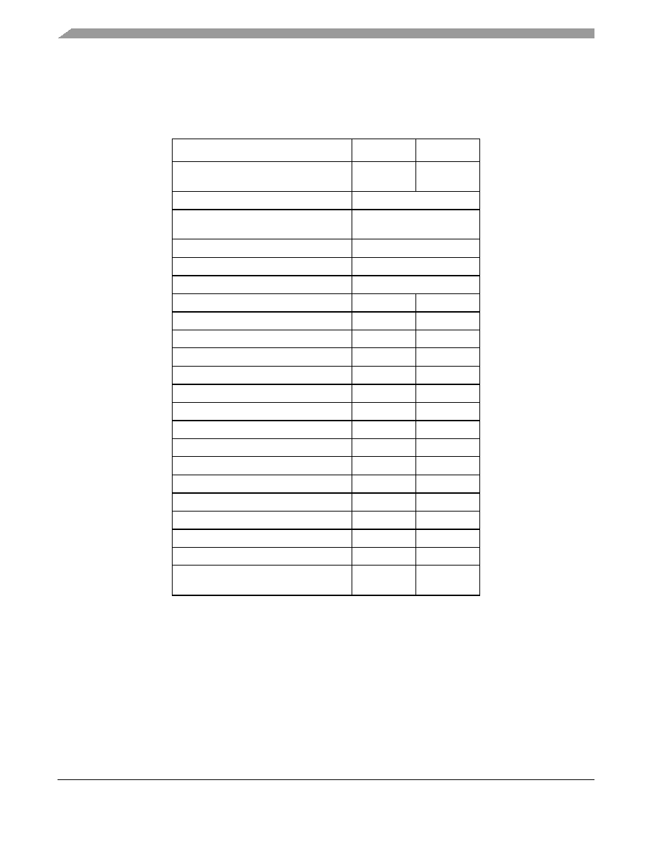
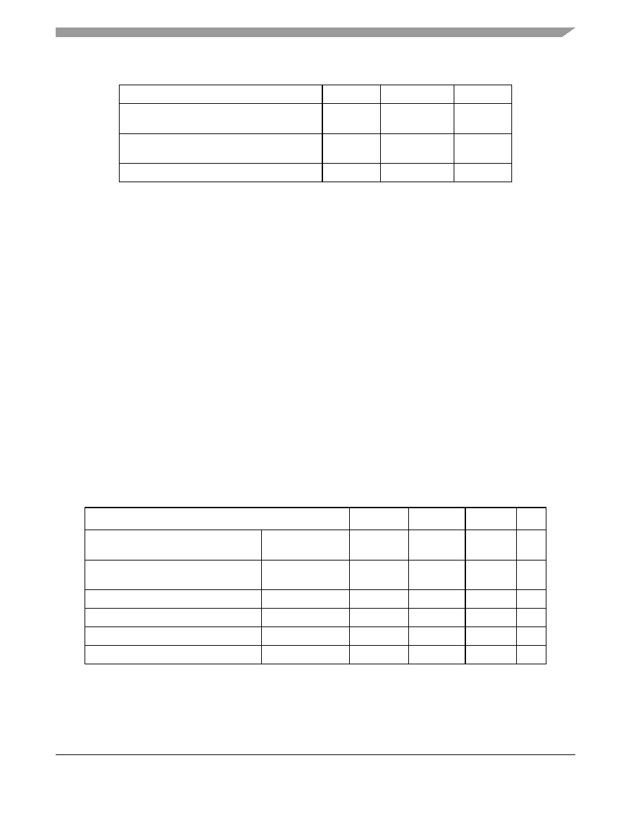
MCF5207/8 Device Configurations
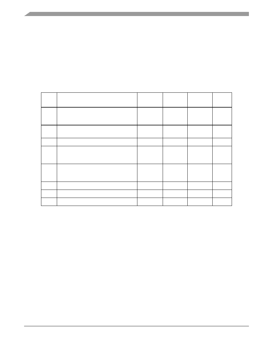
The following table compares the two devices described in this document:
Table 1. MCF5207 & MCF5208 Configurations
Module
MCF5207
MCF5208
Version 2 ColdFire Core with EMAC
(Enhanced Multiply-Accumulate Unit)
x
x
Core (System) Clock
up to 166.67 MHz
Peripheral and External Bus Clock
(Core clock
˜ 2)
up to 83.33 MHz
Performance (Dhrystone/2.1 MIPS)
up to 159
Instruction/Data Cache
8 Kbytes
Static RAM (SRAM)
16 Kbytes
SDR/DDR SDRAM Controller
x
x
Fast Ethernet Controller (FEC)
--
x
Low-Power Management Module
x
x
UARTs
3
3
I
2
C
x
x
QSPI
x
x
32-bit DMA Timers
4
4
Watchdog Timer (WDT)
x
x
Periodic Interrupt Timers (PIT)
4
4
Edge Port Module (EPORT)
x
x
Interrupt Controllers (INTC)
1
1
16-channel Direct Memory Access (DMA)
x
x
FlexBus External Interface
x
x
General Purpose I/O Module (GPIO)
x
x
JTAG - IEEE
Æ
1149.1 Test Access Port
x
x
Package
144 LQFP
144 MAPBGA
160 QFP
196 MAPBGA
Ordering Information
MCF5208 ColdFire
Æ
Microprocessor Data Sheet, Rev. 0.5
Preliminary
Freescale Semiconductor
3
2
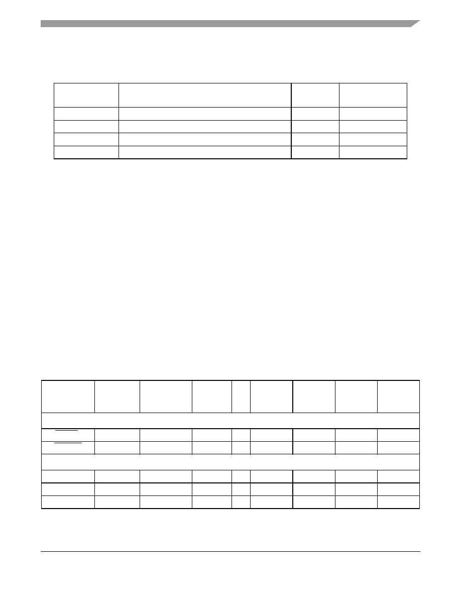
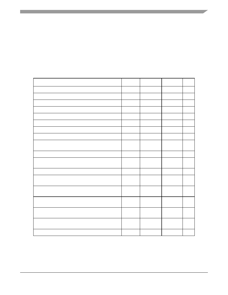
Ordering Information
3
Signal Descriptions
The following table lists all the MCF5208 pins grouped by function. The "Dir" column is the direction for
the primary function of the pin only. Refer to
Section 4, "Mechanicals and Pinouts,"
for package diagrams.
For a more detailed discussion of the MCF5208 signals, consult the MCF5208 Reference Manual
(MCF5208RM).
NOTE
In this table and throughout this document a single signal within a group is
designated without square brackets (i.e., A23), while designations for
multiple signals within a group use brackets (i.e., A[23:21]) and is meant to
include all signals within the two bracketed numbers when these numbers
are separated by a colon.
NOTE
The primary functionality of a pin is not necessarily its default functionality.
Pins that are muxed with GPIO will default to their GPIO functionality.
Table 2. Orderable Part Numbers
Freescale Part
Number
Description
Speed
Temperature
MCF5207CAG166
MCF5207 RISC Microprocessor, 144 LQFP
166.67 MHz
≠40
∞
to +85
∞
C
MCF5207CVM166
MCF5207 RISC Microprocessor, 144 MAPBGA
166.67 MHz
≠40
∞
to +85
∞
C
MCF5208CAB166
MCF5208 RISC Microprocessor, 160 QFP
166.67 MHz
≠40
∞
to +85
∞
C
MCF5208CVM166
MCF5208 RISC Microprocessor, 196 MAPBGA
166.67 MHz
≠40
∞
to +85
∞
C
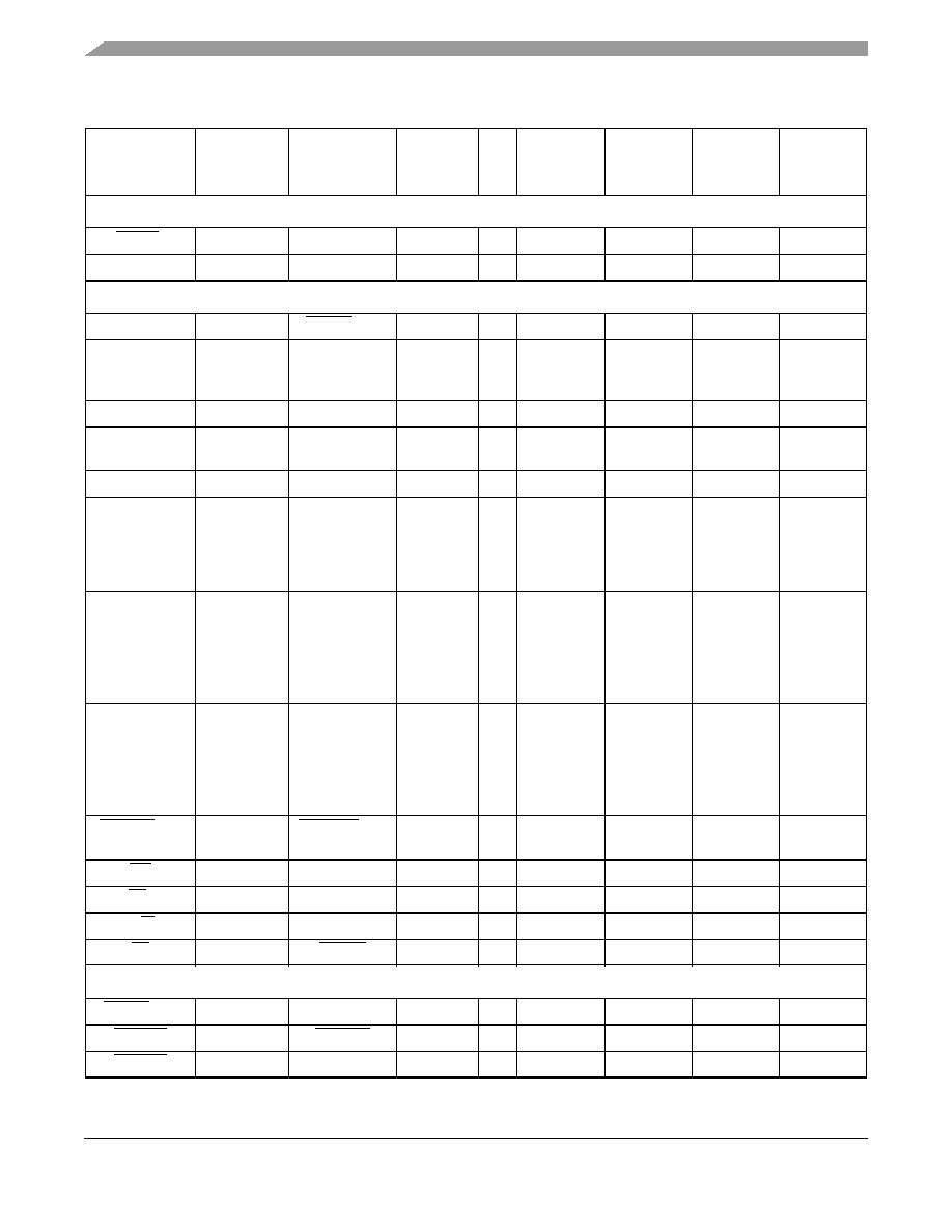
Table 3. MCF5207/8 Signal Information and Muxing
Signal Name
GPIO
Alternate 1
Alternate 2
Dir.
1
MCF5207
144
LQFP
MCF5207
144
MAPBGA
MCF5208
160
QFP
MCF5208
196
MAPBGA
Reset
RESET
2
--
--
--
I
82
J10
90
J14
RSTOUT
--
--
--
O
74
M12
82
N14
Clock
EXTAL
--
--
--
I
78
K12
86
L14
XTAL
--
--
--
O
80
J12
88
K14
FB_CLK
--
--
--
O
34
L1
40
N1
MCF5208 ColdFire
Æ
Microprocessor Data Sheet, Rev. 0.5
Preliminary
Signal Descriptions
Freescale Semiconductor
4
Mode Selection
RCON
2
--
--
--
I
144
C4
160
C3
DRAMSEL
--
--
--
I
79
H10
87
K11
FlexBus
A[23:22]
--
FB_CS[5:4]
--
O
118, 117
B9, A10
126, 125
B11, A11
A[21:16]
--
--
--
O
116≠114,
112, 108,
107
C9, A11,
B10, A12,
C11, B11
124, 123,
122, 120,
116, 115
B12, A12,
A13, B13,
B14, C13
A[15:14]
--
SD_BA[1:0]
--
O
106, 105
B12, C12
114, 113
C14, D12
A[13:11]
--
SD_A[13:11]
--
O
104≠102
D11, E10,
D12
112, 111,
110
D13, D14,
E11
A10
--
--
--
O
101
C10
109
E12
A[9:0]
--
SD_A[9:0]
--
O
100≠91
E11, D9,
E12, F10,
F11, E9,
F12, G10,
G12, F9
108≠99
E13, E14,
F11≠F14,
G11≠G14
D[31:16]
--
SD_D[31:16]
3
--
O
21≠28,
40≠47
F1, F2, G1,
G2, G4, G3,
H1, H2, K3,
L2, L3, K2,
M3, J4, M4,
K4
27≠34,
46≠53
J4≠J1,
K4≠K1, M3,
N3, M4, N4,
P4, L5, M5,
N5
D[15:0]
--
FB_D[31:16]
3
--
O
8≠15, 51≠58 B2, B1, C2,
C1, D2, D1,
E2, E1, L5,
K5, L6, J6,
M6, J7, L7,
K7
16≠23,
57≠64
F3≠F1,
G4≠G1, H1,
N6, P6, L7,
M7, N7, P7,
N8, P8
BE/BWE[3:0]
PBE[3:0]
SD_DQM[3:0]
--
O
20, 48, 18,
50
F4, L4, E3,
J5
26, 54, 24,
56
H2, P5, H4,
M6
OE
PBUSCTL3
--
--
O
60
J8
66
M8
TA
2
PBUSCTL2
--
--
I
90
G11
98
H14
R/W
PBUSCTL1
--
--
O
59
K6
65
L8
TS
PBUSCTL0
DACK0
--
O
4
B3
12
E3
Chip Selects
FB_CS[3:2]
PCS[3:2]
--
--
O
119, 120
D7, A9
--
C11, A10
FB_CS1
PCS1
SD_CS1
--
O
121
C8
127
B10
FB_CS0
--
--
--
O
122
B8
128
C10
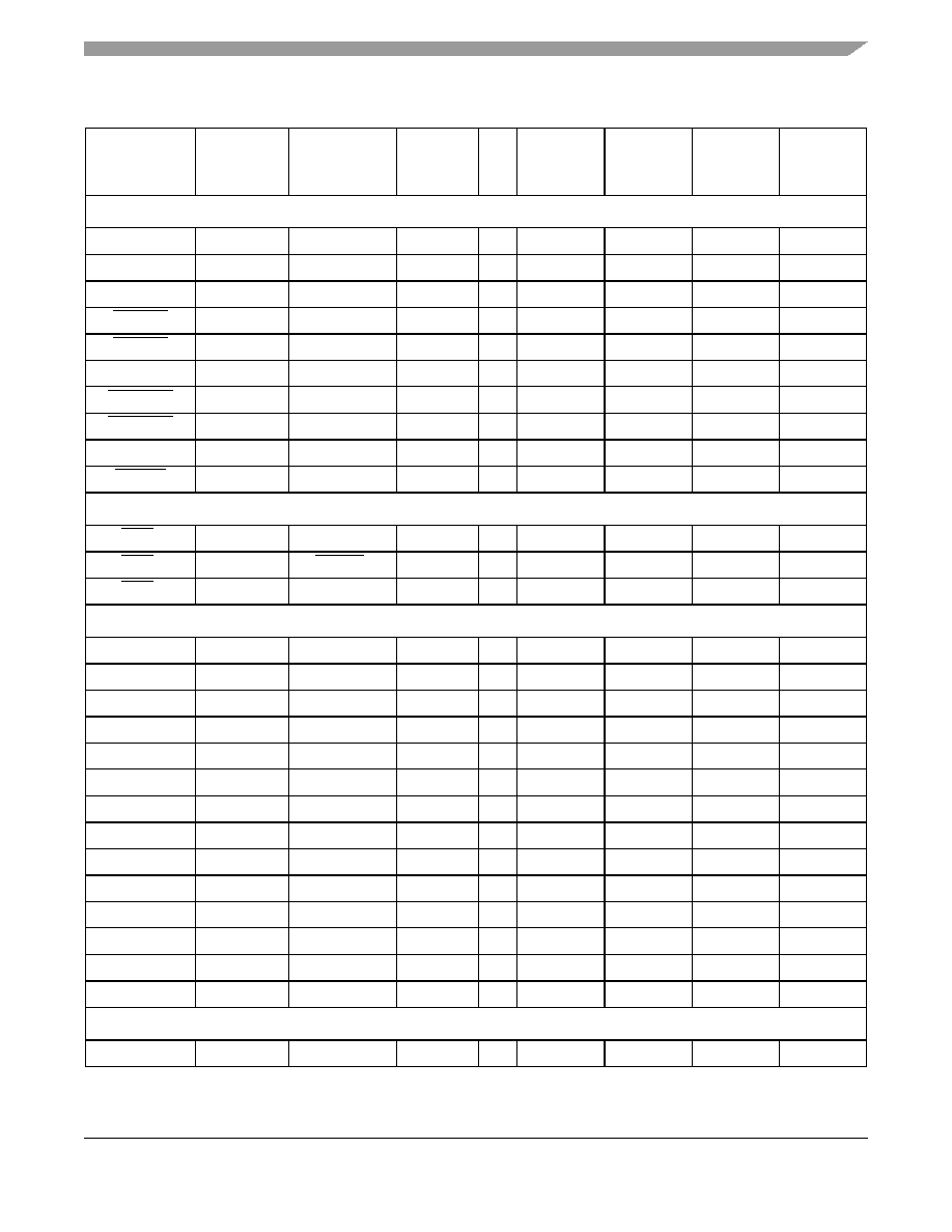
Table 3. MCF5207/8 Signal Information and Muxing (continued)
Signal Name
GPIO
Alternate 1
Alternate 2
Dir.
1
MCF5207
144
LQFP
MCF5207
144
MAPBGA
MCF5208
160
QFP
MCF5208
196
MAPBGA
Signal Descriptions
MCF5208 ColdFire
Æ
Microprocessor Data Sheet, Rev. 0.5
Preliminary
Freescale Semiconductor
5
SDRAM Controller
SD_A10
--
--
--
O
37
M1
43
N2
SD_CKE
--
--
--
O
6
C3
14
E1
SD_CLK
--
--
--
O
31
J1
37
L1
SD_CLK
--
--
--
O
32
K1
38
M1
SD_CS0
--
--
--
O
7
A1
15
F4
SD_DQS[3:2]
--
--
--
O
19, 49
F3, M5
25, 55
H3, L6
SD_SCAS
--
--
--
O
38
M2
44
P2
SD_SRAS
--
--
--
O
39
J2
45
P3
SD_SDR_DQS
--
--
--
O
29
H3
35
L3
SD_WE
--
--
--
O
5
D3
13
E2
External Interrupts Port
4
IRQ7
2
PIRQ7
2
--
--
I
134
A5
142
C7
IRQ4
2
PIRQ4
2
DREQ0
2
--
I
133
C6
141
D7
IRQ1
2
PIRQ1
2
--
--
I
132
B6
140
D8
FEC
FEC_MDC
PFECI2C3
I2C_SCL
2
U2TXD
O
--
--
148
D6
FEC_MDIO
PFECI2C2
I2C_SDA
2
U2RXD
I/O
--
--
147
C6
FEC_TXCLK
PFECH7
--
--
I
--
--
157
B3
FEC_TXEN
PFECH6
--
--
O
--
--
158
A2
FEC_TXD0
PFECH5
--
--
O
--
--
3
B1
FEC_COL
PFECH4
--
--
I
--
--
7
D3
FEC_RXCLK
PFECH3
--
--
I
--
--
154
B4
FEC_RXDV
PFECH2
--
--
I
--
--
153
A4
FEC_RXD0
PFECH1
--
--
I
--
--
152
D5
FEC_CRS
PFECH0
--
--
I
--
--
8
D2
FEC_TXD[3:1]
PFECL[7:5]
--
--
O
--
--
6≠4
C1, C2, B2
FEC_TXER
PFECL4
--
--
O
--
--
156
A3
FEC_RXD[3:1]
PFECL[3:1]
--
--
I
--
--
149≠151
A5, B5, C5
FEC_RXER
PFECL0
--
--
I
--
--
155
C4
I
2
C
I2C_SDA
2
PFECI2C0
2
U2RXD
2
--
I/O
--
--
--
D1
Table 3. MCF5207/8 Signal Information and Muxing (continued)
Signal Name
GPIO
Alternate 1
Alternate 2
Dir.
1
MCF5207
144
LQFP
MCF5207
144
MAPBGA
MCF5208
160
QFP
MCF5208
196
MAPBGA
MCF5208 ColdFire
Æ
Microprocessor Data Sheet, Rev. 0.5
Preliminary
Signal Descriptions
Freescale Semiconductor
6
I2C_SCL
2
PFECI2C1
2
U2TXD
2
--
I/O
--
--
--
E4
DMA
DACK0 and DREQ0 do not have a dedicated bond pads. Please refer to the following pins for muxing:
TS and QSPI_CS2 for DACK0, IRQ4 and QSPI_DIN for DREQ0.
QSPI
QSPI_CS2
PQSPI3
DACK0
U2RTS
O
126
A8
132
D10
QSPI_CLK
PQSPI0
I2C_SCL
2
--
O
127
C7
133
A9
QSPI_DOUT
PQSPI1
I2C_SDA
2
--
O
128
A7
134
B9
QSPI_DIN
PQSPI2
DREQ0
2
U2CTS
I
129
B7
135
C9
Note: The QSPI_CS1 and QSPI_CS0 signals are available on the U1CTS, U1RTS, U0CTS, or U0RTS pins for the 196 and
160-pin packages.
UARTs
U1CTS
PUARTL7
--
--
I
139
B4
--
--
U1RTS
PUARTL6
--
--
O
142
A2
--
--
U1CTS
PUARTL7
DT1IN
QSPI_CS1
I
--
--
136
D9
U1RTS
PUARTL6
DT1OUT
QSPI_CS1
O
--
--
137
C8
U1TXD
PUARTL5
--
--
O
131
A6
139
A8
U1RXD
PUARTL4
--
--
I
130
D6
138
B8
U0CTS
PUARTL3
--
--
I
140
E4
--
--
U0RTS
PUARTL2
--
--
O
141
D5
--
--
U0CTS
PUARTL3
DT0IN
QSPI_CS0
I
--
--
76
N12
U0RTS
PUARTL2
DT0OUT
QSPI_CS0
O
--
--
77
P12
U0TXD
PUARTL1
--
--
O
71
L10
79
P13
U0RXD
PUARTL0
--
--
I
70
M10
78
N13
Note: The UART2 signals are multiplexed on the DMA Timers, QSPI, FEC, and I2C pins.
DMA Timers
DT3IN
PTIMER3
DT3OUT
U2CTS
I
135
B5
143
B7
DT2IN
PTIMER2
DT2OUT
U2RTS
I
136
C5
144
A7
DT1IN
PTIMER1
DT1OUT
U2RXD
I
137
A4
145
A6
DT0IN
PTIMER0
DT0OUT
U2TXD
I
138
A3
146
B6
BDM/JTAG
5
JTAG_EN
6
--
--
--
I
83
J11
91
J13
DSCLK
--
TRST
2
--
I
76
K11
84
L12
Table 3. MCF5207/8 Signal Information and Muxing (continued)
Signal Name
GPIO
Alternate 1
Alternate 2
Dir.
1
MCF5207
144
LQFP
MCF5207
144
MAPBGA
MCF5208
160
QFP
MCF5208
196
MAPBGA
Signal Descriptions
MCF5208 ColdFire
Æ
Microprocessor Data Sheet, Rev. 0.5
Preliminary
Freescale Semiconductor
7
PSTCLK
--
TCLK
2
--
O
64
M7
70
P9
BKPT
--
TMS
2
--
I
75
L12
83
M14
DSI
--
TDI
2
--
I
77
H9
85
K12
DSO
--
TDO
--
O
69
M9
75
M12
DDATA[3:0]
--
--
--
O
--
K9, L9, M11,
M8
--
P11, N11,
M11, P10
PST[3:0]
--
--
--
O
--
L11, L8,
K10, K8
--
N10, M10,
L10, L9
ALLPST
--
--
--
O
67
--
73
--
Test
TEST
6
--
--
--
I
109
--
--
C12
PLL_TEST
--
--
--
I
--
--
--
M13
Power Supplies
EVDD
--
--
--
1, 63, 66, 72,
81, 87, 125
E5≠E6, F5,
G8≠G9,
H7≠H8
2, 9, 69, 72,
80, 89, 95,
131
E5≠E7, F5,
F6, G5, H10,
J9, J10,
K8≠K10,
K13, M9
IVDD
--
--
--
30, 68, 84,
113, 143
D4, D8, H4,
H11, J9
36, 74, 92,
121, 159
J12, D4,
D11, H11,
L4, L11,
PLL_VDD
--
--
--
86
H12
94
H13
SD_VDD
--
--
--
3, 17, 33, 35,
61, 89, 110,
123
E7≠E8, F8,
G5, H5≠H6,
J3
11, 39, 41,
67, 97, 118,
129
E8≠E10, F9,
F10, G10,
H5, J5, J6,
K5≠K7, L2
VSS
--
--
--
2, 16, 36, 62,
65, 73, 88,
111, 124
D10, F6≠F7,
G6≠G7
1, 10, 42, 68,
71, 81, 96,
117, 119,
130
A1, A14,
F7≠F8,
G6≠G9,
H6≠H9,
J7≠J8, L13,
M2, N9, P1,
P14
PLL_VSS
--
--
--
85
--
93
H12
NOTES:
1
Refers to pin's primary function.
2
Pull-up enabled internally on this signal for this mode.
3
Primary functionality selected by asserting the DRAMSEL signal (SDR mode). Alternate functionality selected by negating
the DRAMSEL signal (DDR mode). The GPIO module is not responsible for assigning these pins.
4
GPIO functionality is determined by the edge port module. The GPIO module is only responsible for assigning the alternate
functions.
Table 3. MCF5207/8 Signal Information and Muxing (continued)
Signal Name
GPIO
Alternate 1
Alternate 2
Dir.
1
MCF5207
144
LQFP
MCF5207
144
MAPBGA
MCF5208
160
QFP
MCF5208
196
MAPBGA

MCF5208 ColdFire
Æ
Microprocessor Data Sheet, Rev. 0.5
Preliminary
Mechanicals and Pinouts
Freescale Semiconductor
8
4
Mechanicals and Pinouts
This section contains drawings showing the pinout and the packaging and mechanical characteristics of
the MCF5207 and MCF5208 devices.
NOTE
The mechanical drawings are the latest revisions at the time of publication
of this document. The most up-to-date mechanical drawings can be found at
the product summary page located at
http://www.freescale.com/coldfire
.
5
If JTAG_EN is asserted, these pins default to Alternate 1 (JTAG) functionality. The GPIO module is not responsible for
assigning these pins.
6
Pull-down enabled internally on this signal for this mode.
Mechanicals and Pinouts
MCF5208 ColdFire
Æ
Microprocessor Data Sheet, Rev. 0.5
Preliminary
Freescale Semiconductor
9
4.1
Pinout--144 LQFP
Figure 1
shows a pinout of the MCF5207CAG166 device.
Figure 1. MCF5207CAG166 Pinout Top View (144 LQFP)
RCON
IV
D
D
U1
R
T
S
U0
R
T
S
U0
C
T
S
U1
C
T
S
DT0
I
N
DT1
I
N
DT2
I
N
DT3
I
N
IR
Q
7
IR
Q
4
IR
Q
1
U1
TXD
U1
R
X
D
QSPI_DIN
QSPI_DOU
T
Q
SPI_CLK
QSPI_CS2
EVDD
VSS
SD_VDD
FB
_
C
S
0
FB
_
C
S
1
FB
_
C
S
2
FB
_
C
S
3
A2
3
A2
2
A2
1
A2
0
A1
9
IV
D
D
A1
8
VSS
SD_VDD
TE
S
T
∑
144
143
142
141
140
139
138
137
136
135
134
133
132
131
130
129
128
127
126
125
124
123
122
121
120
119
118
117
116
115
114
113
112
111
110
109
EVDD
1
108
A17
EVSS
2
107
A16
SD_VDD
3
106
A15
TS
4
105
A14
SD_WE
5
104
A13
SD_CKE
6
103
A12
SD_CS
7
102
A11
D15
8
101
A10
D14
9
100
A9
D13
10
99
A8
D12
11
98
A7
D11
12
97
A6
D10
13
96
A5
D9
14
95
A4
D8
15
94
A3
EVSS
16
93
A2
SD_VDD
17
92
A1
BE/BWE1
18
91
A0
SD_DQS1/3
19
90
TA
BE/BWE3
20
89
SD_VDD
D31
21
88
VSS
D30
22
87
EVDD
D29
23
86
PLL_VDD
D28
24
85
PLL_VSS
D27
25
84
IVDD
D26
26
83
JTAG_EN
D25
27
82
RESET
D24
28
81
EVDD
SD_SDR_DQS
29
80
XTAL
IVDD
30
79
DRAMSEL
SD_CLK
31
78
EXTAL
SD_CLK
32
77
TDI/DSI
SD_VDD
33
76
TRST/DSCLK
FB_CLK
34
75
TMS/BKPT
SD_VDD
35
74
RSTOUT
VSS
36
73
VSS
37
38
39
40
41
42
43
44
45
46
47
48
49
50
51
52
53
54
55
56
57
58
59
60
61
62
63
64
65
66
67
68
69
70
71
72
SD_A10
SD_CAS
SD_RAS
D23
D22
D21
D20
D19
D18
D17
D16
BE
/
B
W
E
2
SD_DQS0/2
BE
/
B
W
E
0
D7
D6
D5
D4
D3
D2
D1
D0
R/
W
OE
SD_VDD
VSS
EVDD
TC
L
K
/PSTCLK
VSS
EVDD
ALL_
PST
IVDD
TDO/DSO
U0RXD
U0TXD
EVDD
MCF5208 ColdFire
Æ
Microprocessor Data Sheet, Rev. 0.5
Preliminary
Mechanicals and Pinouts
Freescale Semiconductor
10
4.2
Package Dimensions--144 LQFP
Figure 2
and
Figure 3
show MCF5207CAB166 package dimensions.
Figure 2. MCF5207CAB166 Package Dimensions (Sheet 1 of 2)
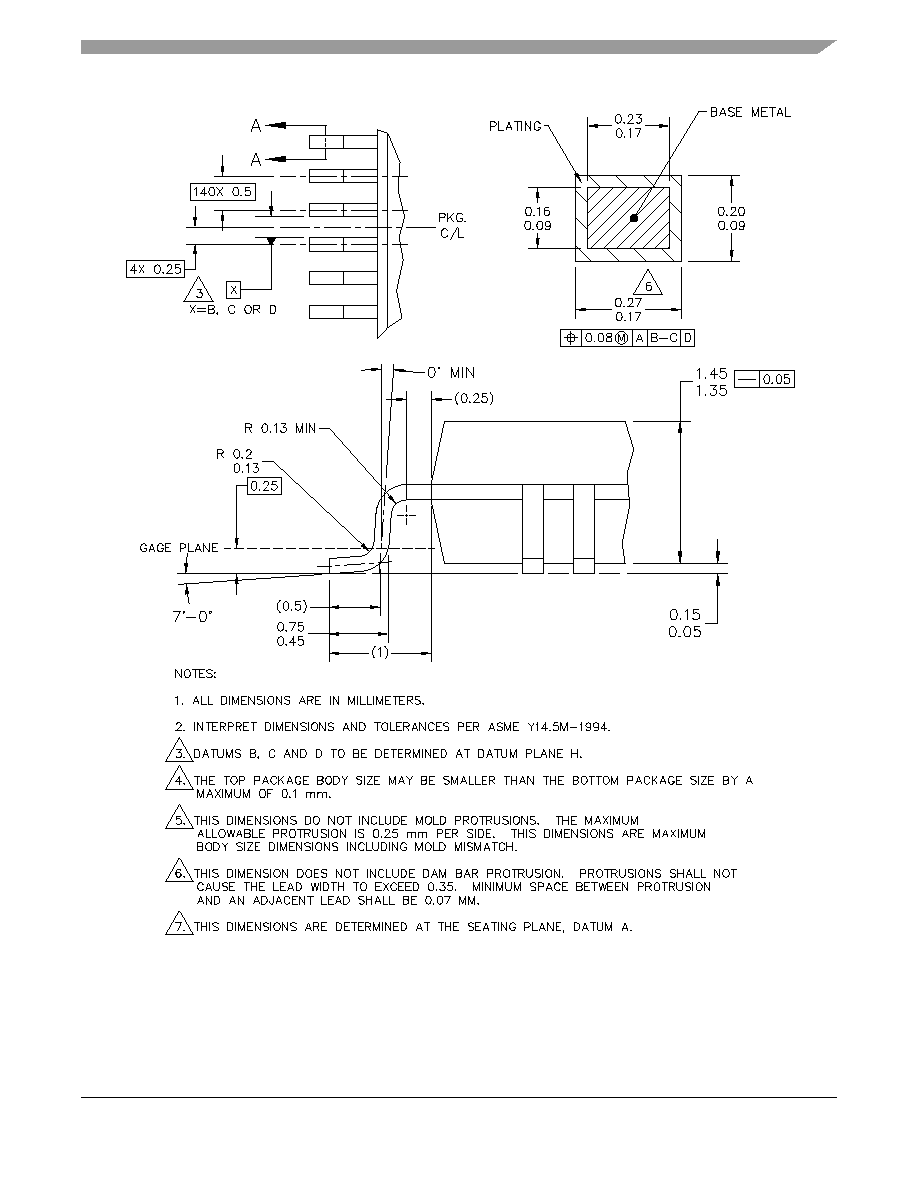
Mechanicals and Pinouts
MCF5208 ColdFire
Æ
Microprocessor Data Sheet, Rev. 0.5
Preliminary
Freescale Semiconductor
11
Figure 3. MCF5207CAB166 Package Dimensions (Sheet 2 of 2)
View A
Section A-A
Rotated 90◊ CW
144 Places
View B
MCF5208 ColdFire
Æ
Microprocessor Data Sheet, Rev. 0.5
Preliminary
Mechanicals and Pinouts
Freescale Semiconductor
12
4.3
Pinout--144 MAPBGA
The pinout of the MCF5207CVM166 device is shown below.
1
2
3
4
5
6
7
8
9
10
11
12
A
SD_CS
U1RTS
DT0IN
DT1IN
IRQ7
U1TXD
QSPI_
DOUT
QSPI_CS2
FB_CS2
A22
A20
A18
A
B
D14
D15
TS
U1CTS
DT3IN
IRQ1
QSPI_DIN
FB_CS0
A23
A19
A16
A15
B
C
D12
D13
SD_CKE
RCON
DT2IN
IRQ4
QSPI_
CLK
FB_CS1
A21
A10
A17
A14
C
D
D10
D11
SD_WE
IVDD
U0RTS
U1RXD
FB_CS3
IVDD
A8
VSS
A13
A11
D
E
D8
D9
BE/BWE1
U0CTS
EVDD
EVDD
SD_VDD
SD_VDD
A4
A12
A9
A7
E
F
D31
D30
SD_DQS1
BE/BWE3
EVDD
VSS
VSS
SD_VDD
A0
A6
A5
A3
F
G
D29
D28
D26
D27
SD_VDD
VSS
VSS
EVDD
EVDD
A2
TA
A1
G
H
D25
D24
SD_SDR_
DQS
IVDD
SD_VDD
SD_VDD
EVDD
EVDD
TDI/DSI
DRAM
SEL
IVDD
PLL_VDD
H
J
SD_CLK
SD_RAS
SD_VDD
D18
BE/BWE0
D4
D2
OE
IVDD
RESET
JTAG_EN
XTAL
J
K
SD_CLK
D20
D23
D16
D6
R/W
D0
PST0
DDATA3
PST1
TRST/
DSCLK
EXTAL
K
L
FB_CLK
D22
D21
BE/BWE2
D7
D5
D1
PST2
DDATA2
U0TXD
PST3
TMS/
BKPT
L
M
SD_A10
SD_CAS
D19
D17
SD_DQS0
D3
TCLK/
PSTCLK
DDATA0
TDO/DSO
U0RXD
DDATA1
RSTOUT
M
1
2
3
4
5
6
7
8
9
10
11
12
Figure 4. MCF5207CVM166 Pinout Top View (144 MAPBGA)
Mechanicals and Pinouts
MCF5208 ColdFire
Æ
Microprocessor Data Sheet, Rev. 0.5
Preliminary
Freescale Semiconductor
13
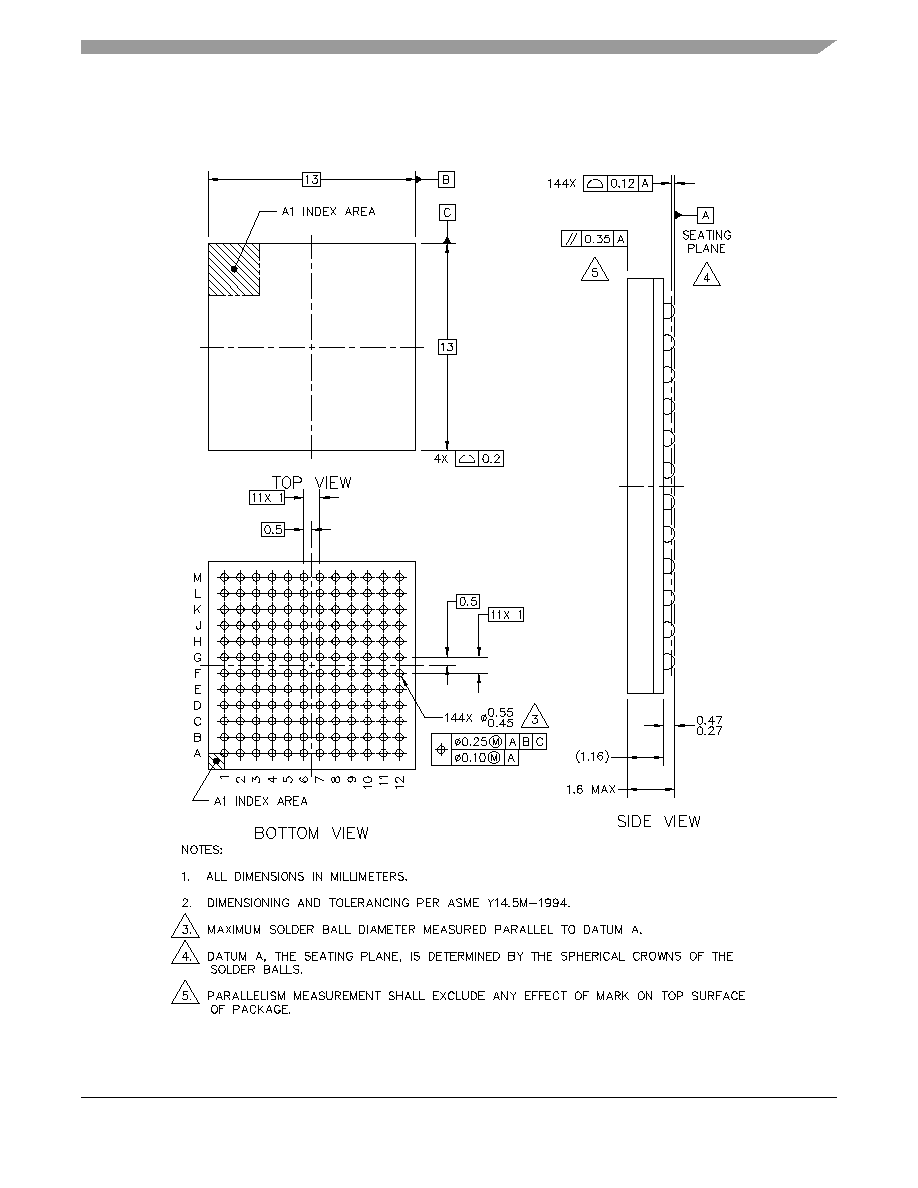
4.4
Package Dimensions--144 MAPBGA
Figure 5
shows the MCF5207CAB166 package dimensions.
Figure 5. MCF5207CAB166 Package Dimensions (144 MAPBGA)
MCF5208 ColdFire
Æ
Microprocessor Data Sheet, Rev. 0.5
Preliminary
Mechanicals and Pinouts
Freescale Semiconductor
14
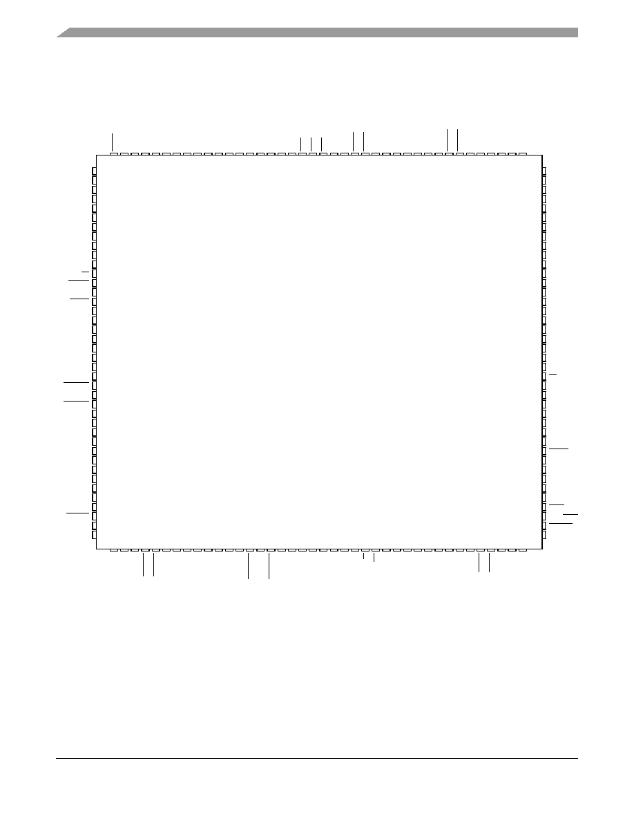
4.5
Pinout--160 QFP
Figure 6
shows a pinout of the MCF5208CAB166 device.
Figure 6. MCF5208CAB166 Pinout Top View (160 QFP)
RCON
IV
D
D
F
E
C
_
TXEN
F
E
C_
T
X
CL
K
F
E
C
_
TXER
F
E
C_
RX
E
R
F
E
C_
RX
C
L
K
F
E
C_
RX
D
V
F
E
C_
RX
D
0
F
E
C_
RX
D
1
F
E
C_
RX
D
2
F
E
C_
RX
D
3
FE
C
_
M
D
C
FE
C
_
M
D
I
O
DT0
I
N
DT1
I
N
DT2
I
N
DT3
I
N
IR
Q
7
IR
Q
4
IR
Q
1
U1
TXD
U1
R
X
D
U1
R
T
S
U1
C
T
S
QSPI_DIN
QSPI_DOU
T
Q
SPI_CLK
QSPI_CS2
EVDD
VSS
SD_VDD
FB
_
C
S
0
FB
_
C
S
1
A2
3
A2
2
A2
1
A2
0
A1
9
IV
D
D
∑
160
159
158
157
156
155
154
153
152
151
150
149
148
147
146
145
144
143
142
141
140
139
138
137
136
135
134
133
132
131
130
129
128
127
126
125
124
123
122
121
VSS
1
120
A18
EVDD
2
119
VSS
FEC_TXD0
3
118
SD_VDD
FEC_TXD1
4
117
VSS
FEC_TXD2
5
116
A17
FEC_TXD3
6
115
A16
FEC_COL
7
114
A15
FEC_CRS
8
113
A14
EVDD
9
112
A13
VSS
10
111
A12
SD_VDD
11
110
A11
TS
12
109
A10
SD_WE
13
108
A9
SD_CKE
14
107
A8
SD_CS
15
106
A7
D15
16
105
A6
D14
17
104
A5
D13
18
103
A4
D12
19
102
A3
D11
20
101
A2
D10
21
100
A1
D9
22
99
A0
D8
23
98
TA
BE/BWE1
24
97
SD_VDD
SD_DQS1/3
25
96
VSS
BE/BWE3
26
95
EVDD
D31
27
94
PLL_VDD
D30
28
93
PLL_VSS
D29
29
92
IVDD
D28
30
91
JTAG_EN
D27
31
90
RESET
D26
32
89
EVDD
D25
33
88
XTAL
D24
34
87
DRAMSEL
SD_SDR_DQS
35
86
EXTAL
IVDD
36
85
TDI/DSI
SD_CLK
37
84
TRST/DSCLK
SD_CLK
38
83
TMS/BKPT
SD_VDD
39
82
RSTOUT
FB_CLK
40
81
VSS
41
42
43
44
45
46
47
48
49
50
51
52
53
54
55
56
57
58
59
60
61
62
63
64
65
66
67
68
69
70
71
72
73
74
75
76
77
78
79
80
SD_VDD
VSS
SD_A10
SD_CAS
SD_RAS
D23
D22
D21
D20
D19
D18
D17
D16
BE
/
B
W
E
2
SD_DQS0/2
BE
/
B
W
E
0
D7
D6
D5
D4
D3
D2
D1
D0
R/
W
OE
SD_VDD
VSS
EVDD
TCLK/PSTCLK
VSS
EVDD
ALL
_
PST
IVDD
TDO/DSO
U0CTS
U0RTS
U0RXD
U0TXD
EVDD
Mechanicals and Pinouts
MCF5208 ColdFire
Æ
Microprocessor Data Sheet, Rev. 0.5
Preliminary
Freescale Semiconductor
15
4.6
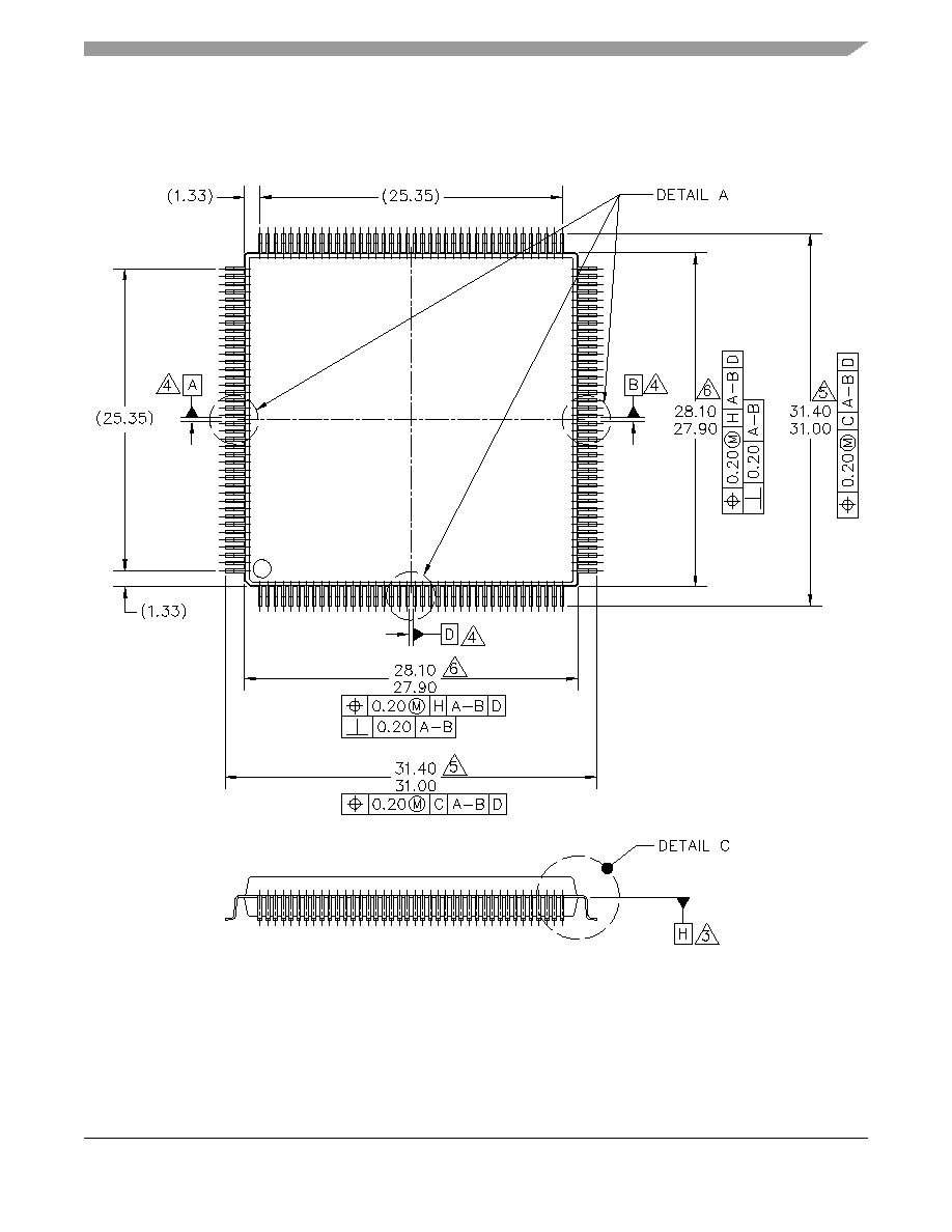
Package Dimensions--160 QFP
The package dimensions of the MCF5208CAB166 device are shown in the figures below.
Figure 7. MCF5208CAB166 Package Dimensions (Sheet 1 of 2)
Top View
MCF5208 ColdFire
Æ
Microprocessor Data Sheet, Rev. 0.5
Preliminary
Mechanicals and Pinouts
Freescale Semiconductor
16
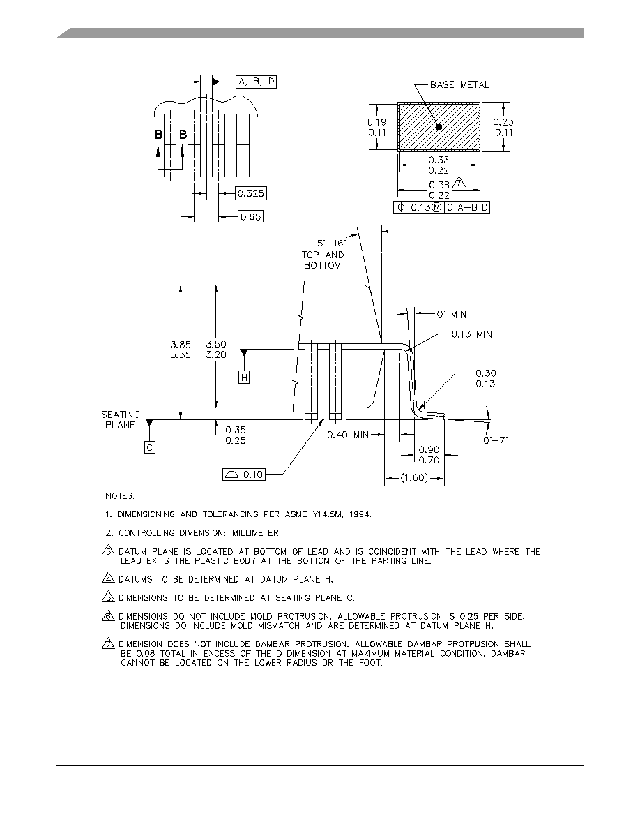
Figure 8. MCF5208CAB166 Package Dimensions (Sheet 2 of 2)
DETAIL A
SECTION B-B
Mechanicals and Pinouts
MCF5208 ColdFire
Æ
Microprocessor Data Sheet, Rev. 0.5
Preliminary
Freescale Semiconductor
17
4.7
Pinout--196 MAPBGA
Figure 6
shows a pinout of the MCF5208CVM166 device.
1
2
3
4
5
6
7
8
9
10
11
12
13
14
A
VSS
FEC_
TXEN
FEC_
TXER
FEC_
RXDV
FEC_
RXD3
DT1IN
DT2IN
U1TXD
QSPI_
CLK
FB_CS2
A22
A20
A19
VSS
A
B
FEC_
TXD0
FEC_
TXD1
FEC_
TXCLK
FEC_
RXCLK
FEC_
RXD2
DT0IN
DT3IN
U1RXD
QSPI_
DOUT
FB_CS1
A23
A21
A18
A17
B
C
FEC_
TXD3
FEC_
TXD2
RCON
FEC_
RXER
FEC_
RXD1
FEC_
MDIO
IRQ7
U1RTS
QSPI_
DIN
FB_CS0
FB_CS3
TEST
A16
A15
C
D
I2C_SDA
FEC_
CRS
FEC_
COL
IVDD
FEC_
RXD0
FEC_
MDC
IRQ4
IRQ1
U1CTS
QSPI_
CS2
IVDD
A14
A13
A12
D
E
SD_CKE
SD_WE
TS
I2C_SCL
EVDD
EVDD
EVDD
SD_VDD
SD_VDD
SD_VDD
A11
A10
A9
A8
E
F
D13
D14
D15
SD_CS
EVDD
EVDD
VSS
VSS
SD_VDD
SD_VDD
A7
A6
A5
A4
F
G
D9
D10
D11
D12
EVDD
VSS
VSS
VSS
VSS
SD_VDD
A3
A2
A1
A0
G
H
D8
BE/
BWE3
SD_
DQS1
BE/
BWE1
SD_VDD
VSS
VSS
VSS
VSS
EVDD
IVDD
PLL_
VSS
PLL_
VDD
TA
H
J
D28
D29
D30
D31
SD_VDD
SD_VDD
VSS
VSS
EVDD
EVDD
NC
IVDD
JTAG_
EN
RESET
J
K
D24
D25
D26
D27
SD_VDD
SD_VDD
SD_VDD
EVDD
EVDD
EVDD
DRAM
SEL
TDI/
DSI
EVDD
XTAL
K
L
SD_CLK
SD_VDD
SD_DR_
DQS
IVDD
D18
SD_
DQS0
D5
R/W
PST0
PST1
IVDD
TRST/
DSCLK
VSS
EXTAL
L
M
SD_CLK
VSS
D23
D21
D17
BE/
BWE0
D4
OE
EVDD
PST2
DDATA1
TDO/
DSO
PLL_
TEST
TMS/
BKPT
M
N
FB_CLK
SD_A10
D22
D20
D16
D7
D3
D1
VSS
PST3
DDATA2
U0CTS
U0RXD
RSTOUT
N
P
VSS
SD_CAS
SD_RAS
D19
BE/
BWE2
D6
D2
D0
TCLK/
PSTCLK
DDATA0
DDATA3
U0RTS
U0TXD
VSS
P
1
2
3
4
5
6
7
8
9
10
11
12
13
14
Figure 9. MCF5208CVM166 Pinout Top View (196 MAPBGA)
MCF5208 ColdFire
Æ
Microprocessor Data Sheet, Rev. 0.5
Preliminary
Preliminary Electrical Characteristics
Freescale Semiconductor
18
4.8
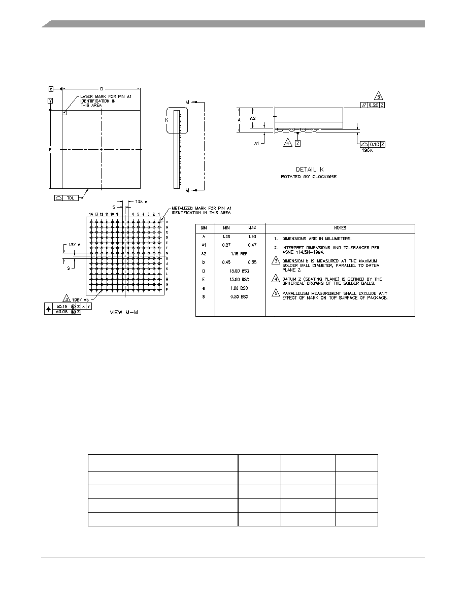
Package Dimensions--196 MAPBGA
The package dimensions for the MCF5208CVM166 device is shown below.
Figure 10. MCF5208CVM166 Package Dimensions (196 MAPBGA)
5
Preliminary Electrical Characteristics
The following electrical specifications are preliminary and are from previous designs or design
simulations. These specifications may not be fully tested or guaranteed at this early stage of the product
life cycle, however for production silicon these specifications will be met. Finalized specifications will be
published after complete characterization and device qualifications have been completed.
5.1
Maximum Ratings
Table 4. Absolute Maximum Ratings
1,
2
Rating
Symbol
Value
Unit
Core Supply Voltage
IV
DD
≠ 0.5 to +2.0
V
CMOS Pad Supply Voltage
EV
DD
≠ 0.3 to +4.0
V
DDR/Memory Pad Supply Voltage
SDV
DD
≠ 0.3 to +4.0
V
PLL Supply Voltage
PLLV
DD
≠ 0.3 to +2.0
V
Top View
Bottom View
Preliminary Electrical Characteristics
MCF5208 ColdFire
Æ
Microprocessor Data Sheet, Rev. 0.5
Preliminary
Freescale Semiconductor
19
5.2
Thermal Characteristics
Table 5
lists thermal resistance values
Digital Input Voltage
3
V
IN
≠ 0.3 to +3.6
V
Instantaneous Maximum Current
Single pin limit (applies to all pins)
3, 4, 5
I
D
25
mA
Operating Temperature Range (Packaged)
T
A
(T
L
- T
H
)
≠ 40 to 85
∞C
Storage Temperature Range
T
stg
≠ 55 to 150
∞C
NOTES:
1
Functional operating conditions are given in
Section 5.4, "DC Electrical Specifications."
Absolute maximum ratings are stress ratings only, and functional operation at the maxima is
not guaranteed. Continued operation at these levels may affect device reliability or cause
permanent damage to the device.
2
This device contains circuitry protecting against damage due to high static voltage or
electrical fields; however, it is advised that normal precautions be taken to avoid application of
any voltages higher than maximum-rated voltages to this high-impedance circuit. Reliability of
operation is enhanced if unused inputs are tied to an appropriate logic voltage level (e.g.,
either V
SS
or EV
DD
).
3
Input must be current limited to the value specified. To determine the value of the required
current-limiting resistor, calculate resistance values for positive and negative clamp voltages,
then use the larger of the two values.
4
All functional non-supply pins are internally clamped to V
SS
and EV
DD
.
5
Power supply must maintain regulation within operating EV
DD
range during instantaneous
and operating maximum current conditions. If positive injection current (V
in
> EV
DD
is greater
than I
DD
, the injection current may flow out of EV
DD
and could result in external power supply
going out of regulation. Insure external EV
DD
load will shunt current greater than maximum
injection current. This will be the greatest risk when the MCU is not consuming power (ex; no
clock). Power supply must maintain regulation within operating EV
DD
range during
instantaneous and operating maximum current conditions.
Table 5. Thermal Characteristics
Characteristic
Symbol
196MBGA
160QFP
Unit
Junction to ambient, natural convection
Four layer board
(2s2p)
JMA
32
1,2
40
1,2
∞C / W
Junction to ambient (@200 ft/min)
Four layer board
(2s2p)
JMA
29
1,2
36
1,2
∞C / W
Junction to board
JB
20
3
25
3
∞C / W
Junction to case
JC
10
4
10
4
∞C / W
Junction to top of package
jt
2
1,5
2
1,5
∞C / W
Maximum operating junction temperature
T
j
105
105
o
C
Table 4. Absolute Maximum Ratings
1,
2
(continued)

MCF5208 ColdFire
Æ
Microprocessor Data Sheet, Rev. 0.5
Preliminary
Preliminary Electrical Characteristics
Freescale Semiconductor
20
The average chip-junction temperature (T
J
) in
∞C can be obtained from:
Eqn. 1
Where:
T
A
= Ambient Temperature, ∞C
Q
JMA
= Package Thermal Resistance, Junction-to-Ambient, ◊C/W
P
D
= P
INT
+ P
I/O
P
INT
= I
DD
◊ IV
DD
, Watts - Chip Internal Power
P
I/O
= Power Dissipation on Input and Output Pins -- User Determined
For most applications P
I/O
< P
INT
and can be ignored. An approximate relationship between P
D
and T
J
(if
P
I/O
is neglected) is:
Eqn. 2
Solving equations 1 and 2 for K gives:
Eqn. 3
where K is a constant pertaining to the particular part. K can be determined from
Equation 3
by measuring
P
D
(at equilibrium) for a known T
A
. Using this value of K, the values of P
D
and T
J
can be obtained by
solving
Equation 1
and
Equation 2
iteratively for any value of T
A
.
5.3
ESD Protection
NOTES:
1
JMA
and
jt
parameters are simulated in conformance with EIA/JESD Standard 51-2 for natural convection.
Freescale recommends the use of
JmA
and power dissipation specifications in the system design to prevent
device junction temperatures from exceeding the rated specification. System designers should be aware that
device junction temperatures can be significantly influenced by board layout and surrounding devices.
Conformance to the device junction temperature specification can be verified by physical measurement in the
customer's system using the
jt
parameter, the device power dissipation, and the method described in
EIA/JESD Standard 51-2.
2
Per JEDEC JESD51-6 with the board horizontal.
3
Thermal resistance between the die and the printed circuit board in conformance with JEDEC JESD51-8. Board
temperature is measured on the top surface of the board near the package.
4
Thermal resistance between the die and the case top surface as measured by the cold plate method (MIL
SPEC-883 Method 1012.1).
5
Thermal characterization parameter indicating the temperature difference between package top and the junction
temperature per JEDEC JESD51-2. When Greek letters are not available, the thermal characterization
parameter is written in conformance with Psi-JT.
Table 6. ESD Protection Characteristics
1,
2
Characteristics
Symbol
Value
Units
ESD Target for Human Body Model
HBM
2000
V
T
J
T
A
P
D
JMA
◊
(
)
+
=
P
D
K
T
J
273
∞C
+
(
)
---------------------------------
=
K
P
D
T
A
273
∞C
◊
(
) Q
JMA
P
D
2
◊
+
◊
=
Preliminary Electrical Characteristics
MCF5208 ColdFire
Æ
Microprocessor Data Sheet, Rev. 0.5
Preliminary
Freescale Semiconductor
21
5.4
DC Electrical Specifications
NOTES:
1
All ESD testing is in conformity with CDF-AEC-Q100 Stress Test Qualification for
Automotive Grade Integrated Circuits.
2
A device is defined as a failure if after exposure to ESD pulses the device no longer meets
the device specification requirements. Complete DC parametric and functional testing is
performed per applicable device specification at room temperature followed by hot
temperature, unless specified otherwise in the device specification.
Table 7. DC Electrical Specifications
Characteristic
Symbol
Min
Max
Unit
Core Supply Voltage
IV
DD
1.4
1.6
V
PLL Supply Voltage
PLLV
DD
1.4
1.6
V
CMOS Pad Supply Voltage
EV
DD
3.0
3.6
V
Mobile DDR/Bus Pad Supply Voltage
SDV
DD
1.65
1.95
V
DDR/Bus Pad Supply Voltage
SDV
DD
2.25
2.75
V
SDR/Bus Pad Supply Voltage
SDV
DD
3.0
3.6
V
CMOS Input High Voltage
EV
IH
2
EV
DD
+ 0.05
V
CMOS Input Low Voltage
EV
IL
-0.05
0.8
V
Mobile DDR/Bus Input High Voltage
SDV
IH
TBD
SDV
DD
+ 0.
05
V
Mobile DDR/Bus Input Low Voltage
SDV
IL
-0.05
TBD
V
DDR/Bus Input High Voltage
SDV
IH
2
SDV
DD
+ 0.
05
V
DDR/Bus Input Low Voltage
SDV
IL
-0.05
0.8
V
Input Leakage Current
V
in
= IV
DD
or V
SS
, Input-only pins
I
in
≠1.0
1.0
µA
CMOS Output High Voltage
I
OH
= ≠5.0 mA
EV
OH
EV
DD
- 0.4
--
V
CMOS Output Low Voltage
I
OL
= 5.0 mA
EV
OL
--
0.4
V
DDR/Bus Output High Voltage
I
OH
= ≠5.0 mA
SDV
OH
SDV
DD
- 0.4
--
V
DDR/Bus Output Low Voltage
I
OL
= 5.0 mA
SDV
OL
--
0.4
V
Weak Internal Pull Up Device Current, tested at V
IL
Max.
1
I
APU
-10
- 130
µA
MCF5208 ColdFire
Æ
Microprocessor Data Sheet, Rev. 0.5
Preliminary
Preliminary Electrical Characteristics
Freescale Semiconductor
22
5.4.1
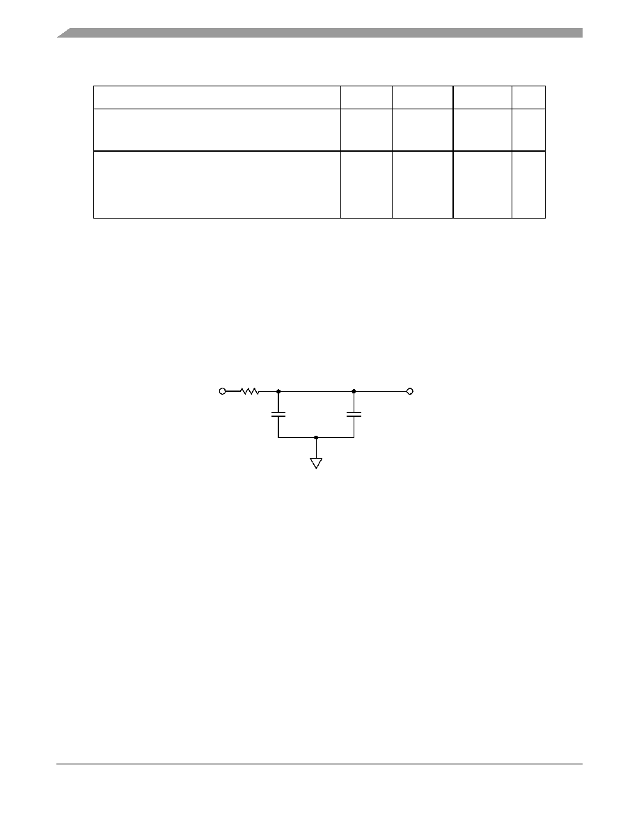
PLL Power Filtering
To further enhance noise isolation, an external filter is strongly recommended for PLL analog V
DD
pins.
The filter shown in
Figure 11
should be connected between the board V
DD
and the PLLV
DD
pins. The
resistor and capacitors should be placed as close to the dedicated PLLV
DD
pin as possible.
Figure 11. System PLL V
DD
Power Filter
5.4.2
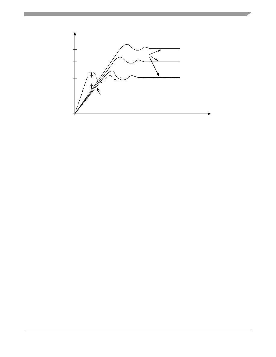
Supply Voltage Sequencing and Separation Cautions
Figure 12
shows situations in sequencing the I/O V
DD
(EV
DD
), SDRAM V
DD
(SDV
DD
), PLL V
DD
(PLLV
DD
), and Core V
DD
(IV
DD
).
Input Capacitance
2
All input-only pins
All input/output (three-state) pins
C
in
--
--
7
7
pF
Core Operating Supply Current
3
Master Mode
LIMP mode
STOP mode
Low Power mode
I
DD
--
170
TBD
1
TBD
mA
mA
mA
mA
NOTES:
1
Refer to the signals section for pins having weak internal pull-up devices.
2
This parameter is characterized before qualification rather than 100% tested.
3
Current measured at maximum system clock frequency, all modules active, and default drive strength with
matching load.
Table 7. DC Electrical Specifications (continued)
Characteristic
Symbol
Min
Max
Unit
Board V
DD
10
0.1 µF
PLL V
DD
Pin
10 µF
GND
Preliminary Electrical Characteristics
MCF5208 ColdFire
Æ
Microprocessor Data Sheet, Rev. 0.5
Preliminary
Freescale Semiconductor
23
Figure 12. Supply Voltage Sequencing and Separation Cautions
The relationship between SDV
DD
and EV
DD
is non-critical during power-up and power-down sequences.
Both SDV
DD
(2.5V or 3.3V) and EV
DD
are specified relative to IV
DD
.
5.4.2.1
Power Up Sequence
If EV
DD
/SDV
DD
are powered up with IV
DD
at 0 V, then the sense circuits in the I/O pads will cause all
pad output drivers connected to the EV
DD
/SDV
DD
to be in a high impedance state. There is no limit on
how long after EV
DD
/SDV
DD
powers up before IV
DD
must powered up. IV
DD
should not lead the EV
DD
,
SDV
DD
or PLLV
DD
by more than 0.4 V during power ramp-up, or there will be high current in the internal
ESD protection diodes. The rise times on the power supplies should be slower than 1
µs to avoid turning
on the internal ESD protection clamp diodes.
The recommended power up sequence is as follows:
1. Use 1
µs or slower rise time for all supplies.
2. IV
DD
/PLLV
DD
and EV
DD
/SDV
DD
should track up to 0.9 V, then separate for the completion of
ramps with EV
DD
/SD V
DD
going to the higher external voltages. One way to accomplish this is to
use a low drop-out voltage regulator.
5.4.2.2
Power Down Sequence
If IV
DD
/PLLV
DD
are powered down first, then sense circuits in the I/O pads will cause all output drivers
to be in a high impedance state. There is no limit on how long after IV
DD
and PLLV
DD
power down before
EV
DD
or SDV
DD
must power down. IV
DD
should not lag EV
DD
, SDV
DD
, or PLLV
DD
going low by more
SDV
DD
(2.5V/1.8V)
Supplies Stable
2
1
3.3V
2.5V
1.5V
0
Time
Notes:
IV
DD
should not exceed EV
DD
, SDV
DD
or PLLV
DD
by more than
0.4 V at any time, including power-up.
Recommended that IV
DD
/PLLV
DD
should track EV
DD
/SDV
DD
up to
0.9 V, then separate for completion of ramps.
Input voltage must not be greater than the supply voltage (EV
DD
, SDV
DD
,
IV
DD
, or PLLV
DD
) by more than 0.5 V at any time, including during power-up.
Use 1
µs or slower rise time for all supplies.
1.
2.
3.
4.
DC P
o
w
e
r Suppl
y
V
o
l
t
a
g
e
IV
DD
, PLLV
DD
EV
DD
, SDV
DD
MCF5208 ColdFire
Æ
Microprocessor Data Sheet, Rev. 0.5
Preliminary
Preliminary Electrical Characteristics
Freescale Semiconductor
24
than 0.4 V during power down or there will be undesired high current in the ESD protection diodes. There
are no requirements for the fall times of the power supplies.
The recommended power down sequence is as follows:
1. Drop IV
DD
/PLLV
DD
to 0 V.
2. Drop EV
DD
/SDV
DD
supplies.
5.5
Oscillator and PLL Electrical Characteristics
5.6
External Interface Timing Characteristics
Table 9
lists processor bus input timings.
NOTE
All processor bus timings are synchronous; that is, input setup/hold and
output delay with respect to the rising edge of a reference clock. The
reference clock is the FB_CLK output.
All other timing relationships can be derived from these values.Timings
listed in
Table 9
are shown in
Figure 14
&
Figure 15
.
Table 8. PLL Electrical Characteristics
Num
Characteristic
Symbol
Min.
Value
Max.
Value
Unit
1
PLL Reference Frequency Range
Crystal reference
External reference
f
ref_crystal
f
ref_ext
TBD
TBD
16
16
MHz
MHz
2
Core frequency
CLKOUT Frequency
1
NOTES:
1
All internal registers retain data at 0 Hz.
f
sys
f
sys/2
TBD
TBD
166.67
83.33
MHz
MHZ
3
Crystal Start-up Time
2, 3
2
This parameter is guaranteed by characterization before qualification rather than 100% tested.
3
Proper PC board layout procedures must be followed to achieve specifications.
t
cst
--
10
ms
4
EXTAL Input High Voltage
Crystal Mode
4
All other modes (External, Limp)
4
This parameter is guaranteed by design rather than 100% tested.
V
IHEXT
V
IHEXT
TBD
TBD
TBD
TBD
V
V
5
EXTAL Input Low Voltage
Crystal Mode
4
All other modes (External, Limp)
V
ILEXT
V
ILEXT
TBD
TBD
TBD
TBD
V
V
6
XTAL Load Capacitance
2
5
30
pF
11
PLL Lock Time
2,5
t
lpll
--
1
ms
14
Duty Cycle of reference
2
t
dc
40
60
%
Preliminary Electrical Characteristics
MCF5208 ColdFire
Æ
Microprocessor Data Sheet, Rev. 0.5
Preliminary
Freescale Semiconductor
25
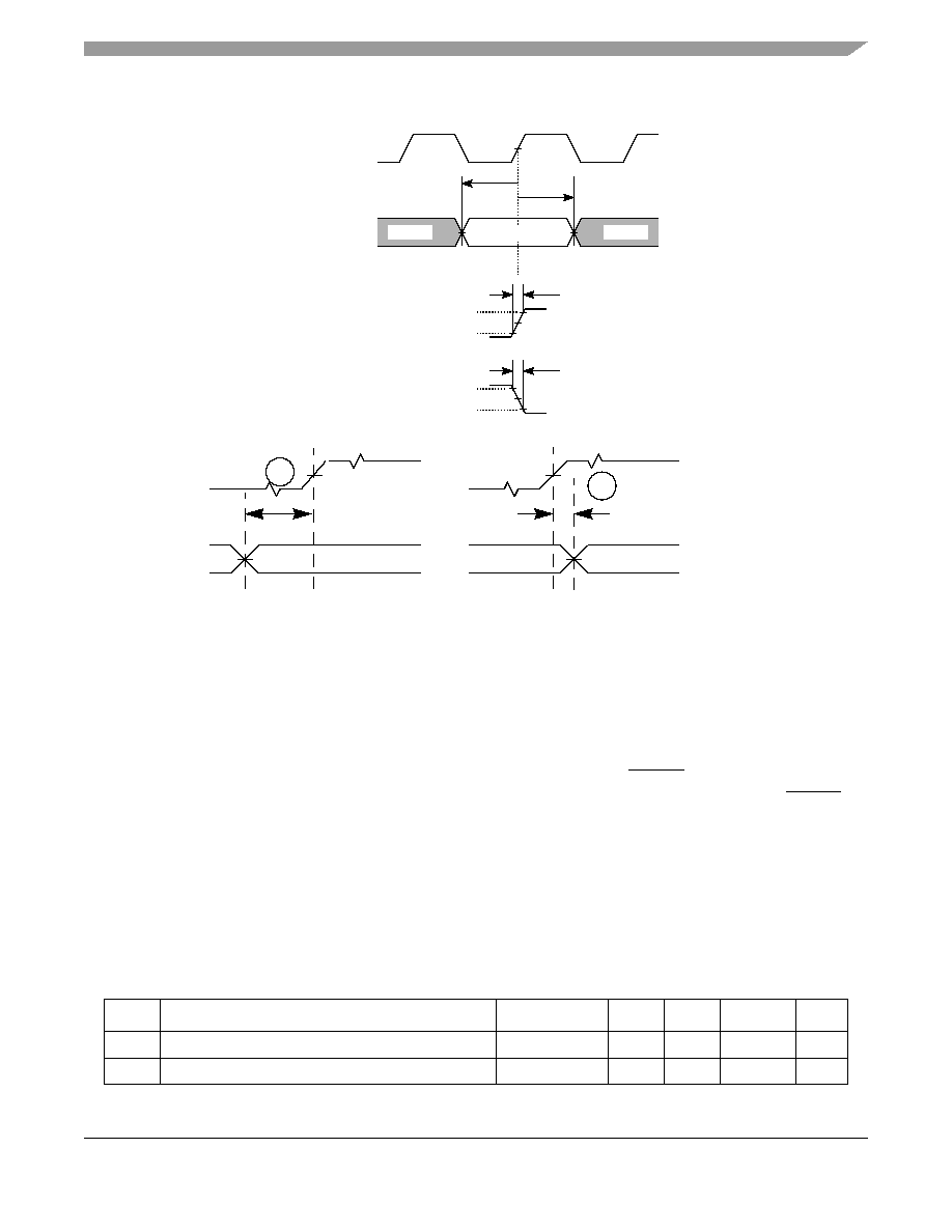
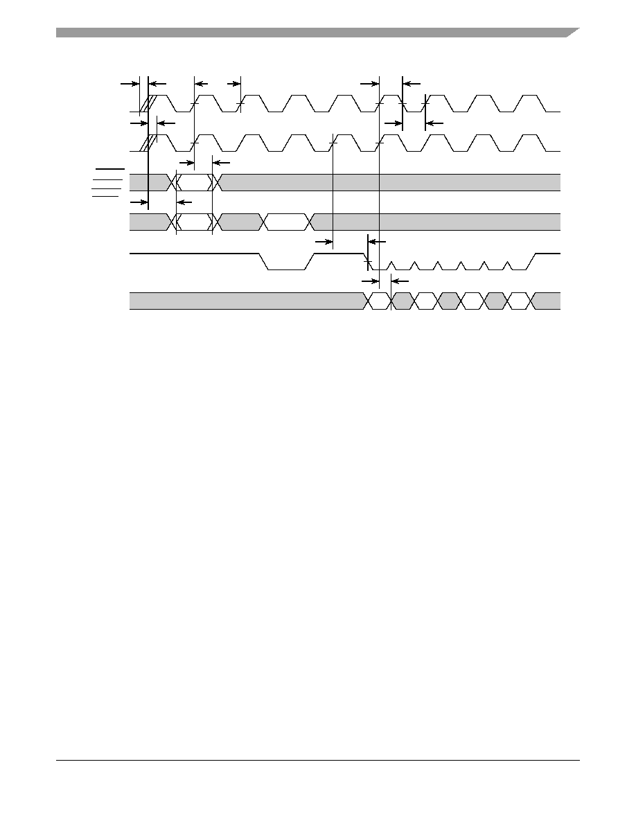
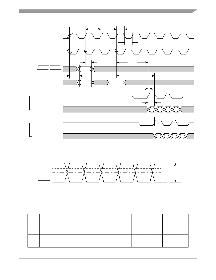
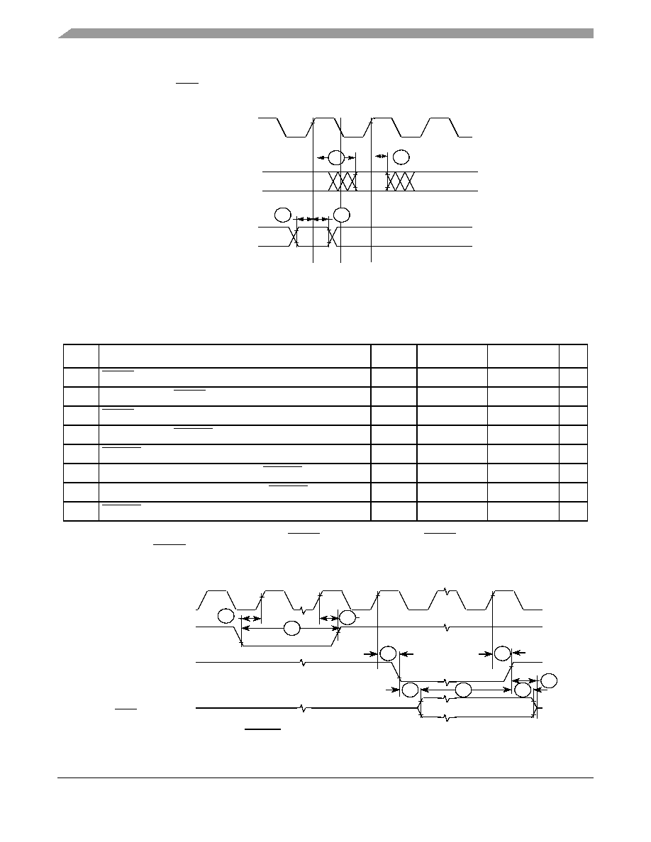
Figure 13. General Input Timing Requirements
5.6.1
FlexBus
A multi-function external bus interface called FlexBus is provided to interface to slave-only devices up to
a maximum bus frequency of 83.33 MHz. It can be directly connected to asynchronous or synchronous
devices such as external boot ROMs, Flash memories, gate-array logic, or other simple target (slave)
devices with little or no additional circuitry. For asynchronous devices a simple chip-select based interface
can be used. The FlexBus interface has six general purpose chip-selects (FB_CS[5:0]) which can be
configured to be distributed between the FlexBus or SDRAM memory interfaces. Chip-select FB_CS[0]
can be dedicated to boot ROM access and can be programmed to be byte (8 bits), word (16 bits), or
longword (32 bits) wide. Control signal timing is compatible with common ROM/Flash memories.
5.6.1.1
FlexBus AC Timing Characteristics
The following timing numbers indicate when data will be latched or driven onto the external bus, relative
to the system clock.
Table 9. FlexBus AC Timing Specifications
Num
Characteristic
Symbol
Min
Max
Unit
Notes
Frequency of Operation
83.33
Mhz
f
sys/2
FB1
Clock Period (FB_CLK)
t
FBCK
12
ns
t
cyc
Invalid
Invalid
FB_CLK(75MHz)
T
SETUP
T
HOLD
Input Setup And Hold
1.5V
t
rise
V
h
= V
IH
V
l
= V
IL
1.5V
1.5V Valid
t
fall
V
h
= V
IH
V
l
= V
IL
Input Rise Time
Input Fall Time
* The timings are also valid for inputs sampled on the negative clock edge.
Inputs
FB_CLK
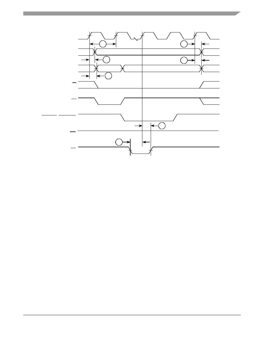
FB4
FB5

MCF5208 ColdFire
Æ
Microprocessor Data Sheet, Rev. 0.5
Preliminary
Preliminary Electrical Characteristics
Freescale Semiconductor
26
Figure 14. FlexBus Read Timing
FB2
Data, and Control Output Valid (A[23:0], D[31:0],
FB_CS[5:0], R/W, TS, BE/BWE[3:0] and OE)
t
FBCHDCV
--
7.0
ns
1
FB3
Data, and Control Output Hold ((A[23:0], D[31:0],
FB_CS[5:0], R/W, TS, BE/BWE[3:0], and OE)
t
FBCHDCI
1
--
ns
1
, 2
FB4
Data Input Setup
t
DVFBCH
3.5
--
ns
FB5
Data Input Hold
t
DIFBCH
0
--
ns
FB6
Transfer Acknowledge (TA) Input Setup
t
CVFBCH
4
--
ns
FB7
Transfer Acknowledge (TA) Input Hold
t
CIFBCH
0
--
ns
FB8
Address Output Valid (A[23:0])
t
FBCHAV
--
6.0
ns
3
FB9
Address Output Hold (A[23:0])
t
FBCHAI
1.0
--
ns
NOTES:
1
Timing for chip selects only applies to the FB_CS[5:0] signals. Please see Section
5.7
, "SDRAM BUS" for SD_CS[1:0]
timing.
2
The FlexBus supports programming an extension of the address hold. Please consult the device reference manual for
more information.
3
These specs are used when the A[23:0] signals are configured as 23-bit, non-muxed FlexBus address signals.
Table 9. FlexBus AC Timing Specifications
Num
Characteristic
Symbol
Min
Max
Unit
Notes
FB_CLK
A[23:0]
D[31:0]
R/W
TS
FB_CSn, BE/BWEn
OE
TA
FB1
A[23:0]
FB2
FB9
FB4
FB5
FB6
FB7
DATA
FB8
Preliminary Electrical Characteristics
MCF5208 ColdFire
Æ
Microprocessor Data Sheet, Rev. 0.5
Preliminary
Freescale Semiconductor
27
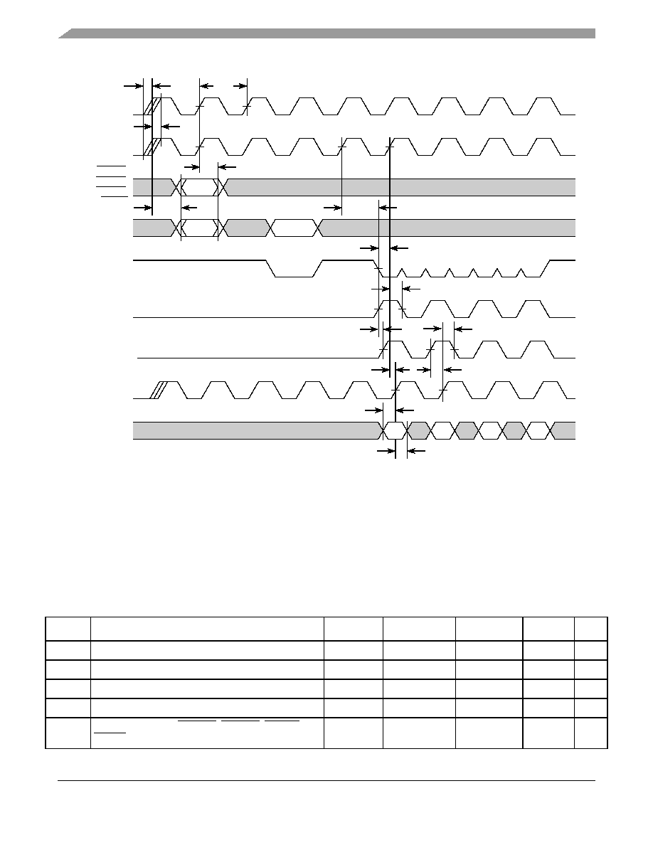
Figure 15. Flexbus Write Timing
5.7
SDRAM Bus
The SDRAM controller supports accesses to main SDRAM memory from any internal master. It supports
either standard SDRAM or double data rate (DDR) SDRAM, but it does not support both at the same time.
The SDRAM controller uses SSTL2 and SSTL3 I/O drivers. Both SSTL drive modes are programmable
for either Class I or Class II drive strength.
5.7.1
SDR SDRAM AC Timing Characteristics
The following timing numbers indicate when data will be latched or driven onto the external bus, relative
to the memory bus clock, when operating in SDR mode on write cycles and relative to SD_DQS on read
cycles. The SDRAM controller is a DDR controller that has an SDR mode. Because it is designed to
support DDR, a DQS pulse must still be supplied to the device for each data beat of an SDR read. The
ColdFire processor accomplishes this by asserting a signal called SD_DQS during read cycles. Care must
be taken during board design to adhere to the following guidelines and specs with regard to the SDR_DQS
signal and its usage.
FB_CLK
A[23:0]
D[31:0]
R/W
TS
FB_CSn, BE/BWEn
TA
FB1
FB2
FB9
FB3
FB6
FB7
OE
FB8
MCF5208 ColdFire
Æ
Microprocessor Data Sheet, Rev. 0.5
Preliminary
Preliminary Electrical Characteristics
Freescale Semiconductor
28
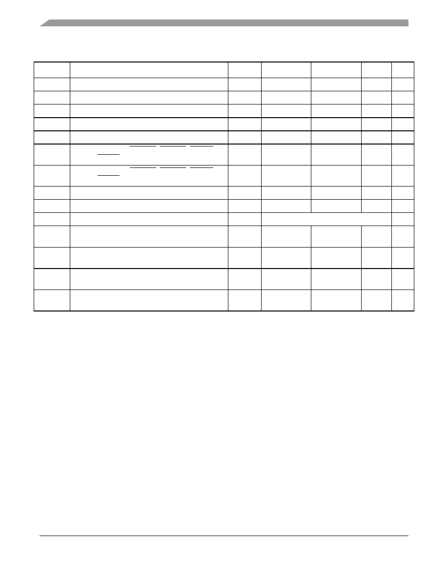
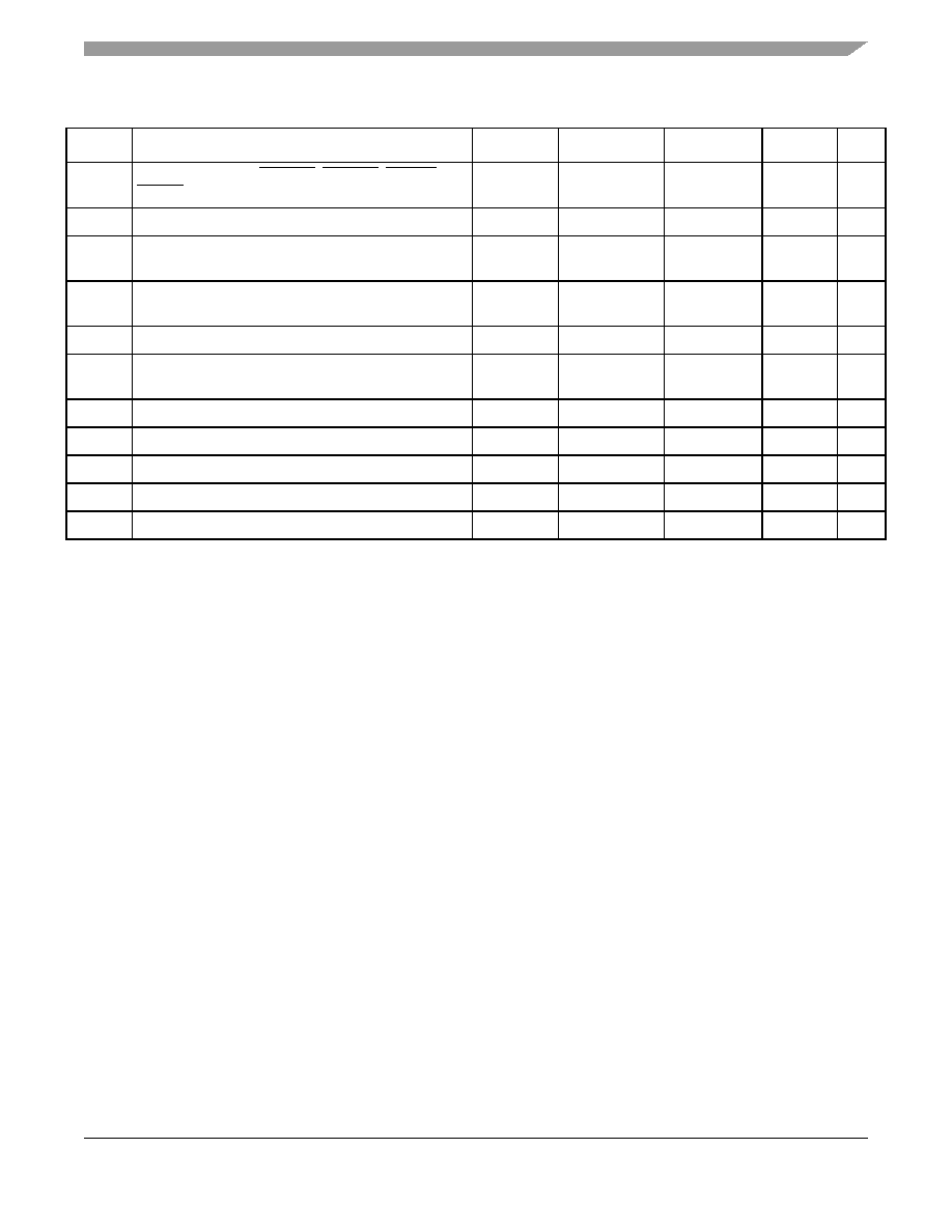
Table 10. SDR Timing Specifications
Symbol
Characteristic
Symbol
Min
Max
Unit
Notes
Frequency of Operation
--
83.33
MHz
1
NOTES:
1
The device supports the same frequency of operation for both FlexBus and SDRAM as that of the internal bus clock. Please see
the PLL chapter of the MCF5208 Reference Manual for more information on setting the SDRAM clock rate.
SD1
Clock Period (t
CK
)
t
SDCK
7.52
12
ns
2
2
SD_CLK is one SDRAM clock in (ns).
SD2
Clock Skew (t
SK
)
t
SDSK
--
TBD
SD3
Pulse Width High (t
CKH
)
t
SDCKH
0.45
0.55
SD_CLK
3
3
Pulse width high plus pulse width low cannot exceed min and max clock period.
SD4
Pulse Width Low (t
CKL
)
t
SDCKL
0.45
0.55
SD_CLK
3
SD5
Address, SD_CKE, SD_CAS, SD_RAS, SD_WE,
SD_BA, SD_CS[1:0] - Output Valid (t
CMV
)
t
SDCHACV
--
0.5
◊ SD_CLK
+ 1.0
ns
SD6
Address, SD_CKE, SD_CAS, SD_RAS, SD_WE,
SD_BA, SD_CS[1:0] - Output Hold (t
CMH
)
t
SDCHACI
2.0
--
ns
SD7
SD_SDR_DQS Output Valid (t
DQSOV
)
t
DQSOV
--
Self timed
ns
4
4
SD_DQS is designed to pulse 0.25 clock before the rising edge of the memory clock. This is a guideline only. Subtle variation from
this guideline is expected. SD_DQS will only pulse during a read cycle and one pulse will occur for each data beat.
SD8
SD_DQS[3:0] input setup relative to SD_CLK (t
DQSIS
) t
DQVSDCH
0.25
◊ SD_CLK 0.40 ◊ SD_CLK
ns
5
5
SDR_DQS is designed to pulse 0.25 clock before the rising edge of the memory clock. This spec is a guideline only. Subtle
variation from this guideline is expected. SDR_DQS will only pulse during a read cycle and one pulse will occur for each data beat.
SD9
SD_DQS[3:2] input hold relative to SD_CLK (t
DQSIH
)
t
DQISDCH
Does not apply. 0.5 SD_CLK fixed width.
6
6
The SDR_DQS pulse is designed to be 0.5 clock in width. The timing of the rising edge is most important. The falling edge does
not affect the memory controller.
SD10
Data (D[31:0]) Input Setup relative to SD_CLK
(reference only) (t
DIS
)
t
DVSDCH
0.25
◊ SD_CLK
--
ns
7
7
Since a read cycle in SDR mode still uses the DQS circuit within the device, it is most critical that the data valid window be centered
1/4 clk after the rising edge of DQS. Ensuring that this happens will result in successful SDR reads. The input setup spec is just
provided as guidance.
SD11
Data Input Hold relative to SD_CLK (reference only)
(t
DIH
)
t
DISDCH
1.0
--
ns
SD12
Data (D[31:0]) and Data Mask(SD_DQM[3:0])
Output Valid (t
DV
)
t
SDCHDMV
--
0.75
◊ SD_CLK
+ 0.5
ns
SD13
Data (D[31:0]) and Data Mask (SD_DQM[3:0]) Output
Hold (t
DH
)
t
SDCHDMI
1.5
--
ns
Preliminary Electrical Characteristics
MCF5208 ColdFire
Æ
Microprocessor Data Sheet, Rev. 0.5
Preliminary
Freescale Semiconductor
29
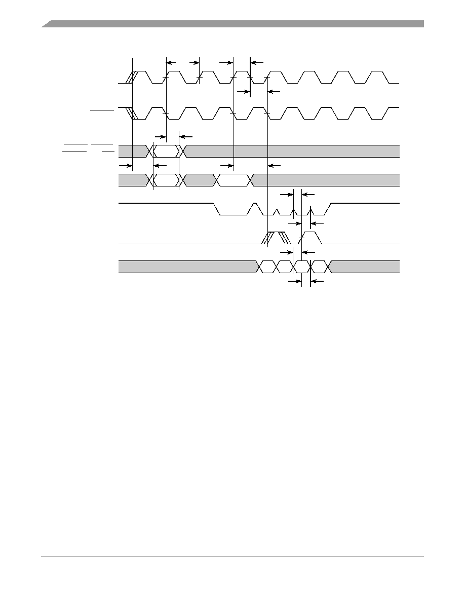
Figure 16. SDR Write Timing
SD_CLK0
SD_CLK1
SDDM
D[31:0]
A[23:0],
SD_BA[1:0]
SD2
CMD
ROW
SD2
SD1
SD5
COL
SD6
WD1
WD2
WD3
WD4
SD13
SD12
SD3
SD4
SD_CSn,
SD_RAS,
SD_WE,
SD_CAS
MCF5208 ColdFire
Æ
Microprocessor Data Sheet, Rev. 0.5
Preliminary
Preliminary Electrical Characteristics
Freescale Semiconductor
30
Figure 17. SDR Read Timing
5.7.2
DDR SDRAM AC Timing Characteristics
When using the SDRAM controller in DDR mode, the following timing numbers must be followed to
properly latch or drive data onto the memory bus. All timing numbers are relative to the four DQS byte
lanes. The following timing numbers are subject to change at anytime, and are only provided to aid in early
board design. Please contact your local Freescale representative if questions develop.
Table 11. DDR Timing Specifications
Num
Characteristic
Symbol
Min
Max
Unit
Notes
Frequency of Operation
83.33
TBD
Mhz
1
DD1
Clock Period (SD_CLK)
t
DDCK
TBD
12
ns
2
DD2
Pulse Width High
t
DDCKH
0.45
0.55
SD_CLK
3
DD3
Pulse Width Low
t
DDCKL
0.45
0.55
SD_CLK
3
DD4
Address, SD_CKE, SD_CAS, SD_RAS, SD_WE,
SD_CS[1:0] - Output Valid
t
SDCHACV
--
0.5
◊ SD_CLK
+ 1.0
ns
4
SD_CLK0
SD_CLK1
SD_CSn,
SDDM
D[31:0]
A[23:0],
SD_RAS,
SD_BA[1:0]
SD2
CMD
ROW
SD2
SD1
SD5
COL
WD1
WD2
WD3
WD4
SD10
3/4 MCLK
SD_DQS
SD_DDQS
Delayed
SD11
SD8
Board Delay
SD9
Board Delay
SD7
tDQS
Reference
SD_CLK
form
Memories
(Measured at Output Pin)
(Measured at Input Pin)
SD6
NOTE: Data driven from memories relative
to delayed memory clock.
SD_WE
SD_CAS,
Preliminary Electrical Characteristics
MCF5208 ColdFire
Æ
Microprocessor Data Sheet, Rev. 0.5
Preliminary
Freescale Semiconductor
31
DD5
Address, SD_CKE, SD_CAS, SD_RAS, SD_WE,
SD_CS[1:0] - Output Hold
t
SDCHACI
2.0
--
ns
DD6
Write Command to first DQS Latching Transition
t
CMDVDQ
1.25
SD_CLK
DD7
Data and Data Mask Output Setup (DQ-->DQS)
Relative to DQS (DDR Write Mode)
t
DQDMV
1.5
--
ns
5
6
DD8
Data and Data Mask Output Hold (DQS-->DQ)
Relative to DQS (DDR Write Mode)
t
DQDMI
1.0
--
ns
7
DD9
Input Data Skew Relative to DQS (Input Setup)
t
DVDQ
--
1
ns
8
DD10
Input Data Hold Relative to DQS.
t
DIDQ
0.25
◊ SD_CLK
+ 0.5ns
--
ns
9
DD11
DQS falling edge from SDCLK rising (output hold time)
t
DQLSDCH
0.5
--
ns
DD12
DQS input read preamble width (t
RPRE
)
t
DQRPRE
0.9
1.1
SD_CLK
DD13
DQS input read postamble width (t
RPST
)
t
DQRPST
0.4
0.6
SD_CLK
DD14
DQS output write preamble width (t
WPRE
)
t
DQWPRE
0.25
--
SD_CLK
DD15
DQS output write postamble width (t
WPST
)
t
DQWPST
0.4
0.6
SD_CLK
NOTES:
1
The frequency of operation is either 2x or 4x the FB_CLK frequency of operation. FlexBus and SDRAM clock operate at the same
frequency as the internal bus clock.
2
SD_CLK is one SDRAM clock in (ns).
3
Pulse width high plus pulse width low cannot exceed min and max clock period.
4
Command output valid should be 1/2 the memory bus clock (SD_CLK) plus some minor adjustments for process, temperature, and
voltage variations.
5
This specification relates to the required input setup time of today's DDR memories. The device's output setup should be larger
than the input setup of the DDR memories. If it is not larger, then the input setup on the memory will be in violation.
MEM_DATA[31:24] is relative to MEM_DQS[3], MEM_DATA[23:16] is relative to MEM_DQS[2], MEM_DATA[15:8] is relative to
MEM_DQS[1], and MEM_[7:0] is relative MEM_DQS[0].
6
The first data beat will be valid before the first rising edge of DQS and after the DQS write preamble. The remaining data beats will
be valid for each subsequent DQS edge.
7
This specification relates to the required hold time of today's DDR memories. MEM_DATA[31:24] is relative to MEM_DQS[3],
MEM_DATA[23:16] is relative to MEM_DQS[2], MEM_DATA[15:8] is relative to MEM_DQS[1], and MEM_[7:0] is relative
MEM_DQS[0].
8
Data input skew is derived from each DQS clock edge. It begins with a DQS transition and ends when the last data line becomes
valid. This input skew must include DDR memory output skew and system level board skew (due to routing or other factors).
9
Data input hold is derived from each DQS clock edge. It begins with a DQS transition and ends when the first data line becomes
invalid.
Table 11. DDR Timing Specifications (continued)
Num
Characteristic
Symbol
Min
Max
Unit
Notes
MCF5208 ColdFire
Æ
Microprocessor Data Sheet, Rev. 0.5
Preliminary
Preliminary Electrical Characteristics
Freescale Semiconductor
32
Figure 18. DDR Write Timing
SD_CLK
SD_CSn, SD_WE,
DM3/DM2
D[31:24]/D[23:16]
A[13:0]
SD_RAS, SD_CAS
CMD
ROW
DD1
DD5
DD4
COL
WD1 WD2 WD3 WD4
DD7
SD_DQS3/SD_DQS2
DD8
DD8
DD7
SD_CLK
DD3
DD2
DD6
Preliminary Electrical Characteristics
MCF5208 ColdFire
Æ
Microprocessor Data Sheet, Rev. 0.5
Preliminary
Freescale Semiconductor
33
Figure 19. DDR Read Timing
Figure 20
shows the DDR clock crossover specifications.
Figure 20. DDR Clock Crossover Timing
5.8
General Purpose I/O Timing
Table 12. GPIO Timing
1
Num
Characteristic
Symbol
Min
Max
Unit
G1
FB_CLK High to GPIO Output Valid
t
CHPOV
--
8
ns
G2
FB_CLK High to GPIO Output Invalid
t
CHPOI
1.5
--
ns
G3
GPIO Input Valid to FB_CLK High
t
PVCH
8
--
ns
G4
FB_CLK High to GPIO Input Invalid
t
CHPI
1.5
--
ns
SD_CLK
SD_CSn, SD_WE,
SD_DQS3/SD_DQS2
D[31:24]/D[23:16]
A[13:0]
SD_RAS, SD_CAS
CMD
ROW
DD1
DD5
DD4
WD1 WD2 WD3 WD4
SD_DQS3/SD_DQS2
DD9
SD_CLK
DD3
DD2
D[31:24]/D[23:16]
WD1 WD2 WD3 WD4
DD10
CL=2
CL=2.5
COL
DQS Read
Preamble
DQS Read
Postamble
DQS Read
Preamble
DQS Read
Postamble
CL = 2.5
CL =
2
SD_CLK
SD_CLK
V
IX
V
MP
V
IX
V
ID
MCF5208 ColdFire
Æ
Microprocessor Data Sheet, Rev. 0.5
Preliminary
Preliminary Electrical Characteristics
Freescale Semiconductor
34
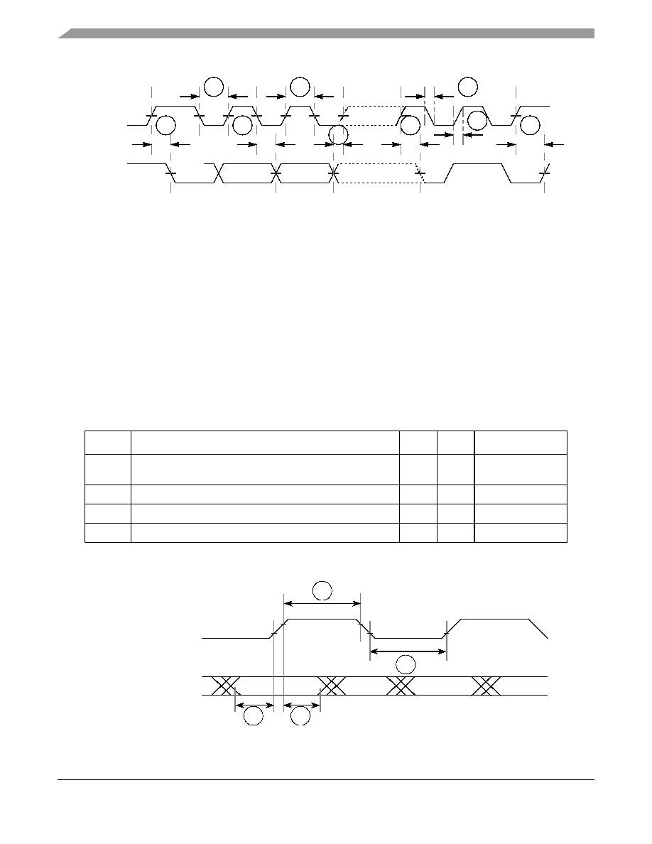
Figure 21. GPIO Timing
5.9
Reset and Configuration Override Timing
Figure 22. RESET and Configuration Override Timing
NOTES:
1
GPIO spec cover: IRQn, UART and Timer pins.
Table 13. Reset and Configuration Override Timing
Num
Characteristic
Symbol
Min
Max
Unit
R1
RESET Input valid to FB_CLK High
t
RVCH
9
--
ns
R2
FB_CLK High to RESET Input invalid
t
CHRI
1.5
--
ns
R3
RESET Input valid Time
1
NOTES:
1
During low power STOP, the synchronizers for the RESET input are bypassed and RESET is asserted asynchronously to
the system. Thus, RESET must be held a minimum of 100 ns.
t
RIVT
5
--
t
CYC
R4
FB_CLK High to RSTOUT Valid
t
CHROV
--
10
ns
R5
RSTOUT valid to Config. Overrides valid
t
ROVCV
0
--
ns
R6
Configuration Override Setup Time to RSTOUT invalid
t
COS
20
--
t
CYC
R7
Configuration Override Hold Time after RSTOUT invalid
t
COH
0
--
ns
R8
RSTOUT invalid to Configuration Override High Impedance
t
ROICZ
--
1
t
CYC
G1
FB_CLK
GPIO Outputs
G2
G3
G4
GPIO Inputs
R1
R2
FB_CLK
RESET
RSTOUT
R3
R4
R8
R7
R6
R5
Configuration Overrides*:
R4
(RCON, Override pins)
Preliminary Electrical Characteristics
MCF5208 ColdFire
Æ
Microprocessor Data Sheet, Rev. 0.5
Preliminary
Freescale Semiconductor
35
NOTE
Refer to the MCF5208 Reference Manual for more information.
5.10 I
2
C Input/Output Timing Specifications
Table 14
and
Table 15
list specifications for the I
2
C input and output timing parameters.
Table 14. I
2
C Input Timing Specifications between I2C_SCL and I2C_SDA
Num
Characteristic
Min
Max
Units
I1
Start condition hold time
2
--
t
cyc
I2
Clock low period
8
--
t
cyc
I3
I2C_SCL/I2C_SDA rise time (V
IL
= 0.5 V to V
IH
= 2.4 V)
--
1
ms
I4
Data hold time
0
--
ns
I5
I2C_SCL/I2C_SDA fall time (V
IH
= 2.4 V to V
IL
= 0.5 V)
--
1
ms
I6
Clock high time
4
--
t
cyc
I7
Data setup time
0
--
ns
I8
Start condition setup time (for repeated start condition only)
2
--
t
cyc
I9
Stop condition setup time
2
--
t
cyc
Table 15. I
2
C Output Timing Specifications between I2C_SCL and I2C_SDA
Num
Characteristic
Min
Max
Units
I1
1
NOTES:
1
Note: Output numbers depend on the value programmed into the IFDR; an IFDR programmed with the
maximum frequency (IFDR = 0x20) results in minimum output timings as shown in Table A-16. The I
2
C
interface is designed to scale the actual data transition time to move it to the middle of the I2C_SCL low
period. The actual position is affected by the prescale and division values programmed into the IFDR;
however, the numbers given in Table A-16 are minimum values.
Start condition hold time
6
--
t
cyc
I2
1.
Clock low period
10
--
t
cyc
I3
2
2
Because I2C_SCL and I2C_SDA are open-collector-type outputs, which the processor can only actively
drive low, the time I2C_SCL or I2C_SDA take to reach a high level depends on external signal
capacitance and pull-up resistor values.
I2C_SCL/I2C_SDA rise time (V
IL
= 0.5 V to V
IH
= 2.4 V)
--
--
µs
I4
1.
Data hold time
7
--
t
cyc
I5
3
3
Specified at a nominal 50-pF load.
I2C_SCL/I2C_SDA fall time (V
IH
= 2.4 V to V
IL
= 0.5 V)
--
3
ns
I6
1.
Clock high time
10
--
t
cyc
I7
1.
Data setup time
2
--
t
cyc
I8
1.
Start condition setup time (for repeated start condition only)
20
--
t
cyc
I9
1.
Stop condition setup time
10
--
t
cyc
MCF5208 ColdFire
Æ
Microprocessor Data Sheet, Rev. 0.5
Preliminary
Preliminary Electrical Characteristics
Freescale Semiconductor
36
Figure 23. I
2
C Input/Output Timings
5.11 Fast Ethernet AC Timing Specifications
MII signals use TTL signal levels compatible with devices operating at either 5.0 V or 3.3 V.
5.11.1 MII Receive Signal Timing (FEC_RXD[3:0], FEC_RXDV,
FEC_RXER, and FEC_RXCLK)
The receiver functions correctly up to a FEC_RXCLK maximum frequency of 25 MHz +1%. There is no
minimum frequency requirement. In addition, the processor clock frequency must exceed twice the
FEC_RXCLK frequency.
Table 16
lists MII receive channel timings.
Figure 24
shows MII receive signal timings listed in
Table 16
.
Figure 24. MII Receive Signal Timing Diagram
Table 16. MII Receive Signal Timing
Num
Characteristic
Min
Max
Unit
M1
FEC_RXD[3:0], FEC_RXDV, FEC_RXER to FEC_RXCLK
setup
5
--
ns
M2
FEC_RXCLK to FEC_RXD[3:0], FEC_RXDV, FEC_RXER hold
5
--
ns
M3
FEC_RXCLK pulse width high
35%
65%
FEC_RXCLK period
M4
FEC_RXCLK pulse width low
35%
65%
FEC_RXCLK period
I2
I6
I1
I4
I7
I8
I9
I5
I3
I2C_SCL
I2C_SDA
M1
M2
FEC_RXCLK (input)
FEC_RXD[3:0] (inputs)
FEC_RXDV
FEC_RXER
M3
M4
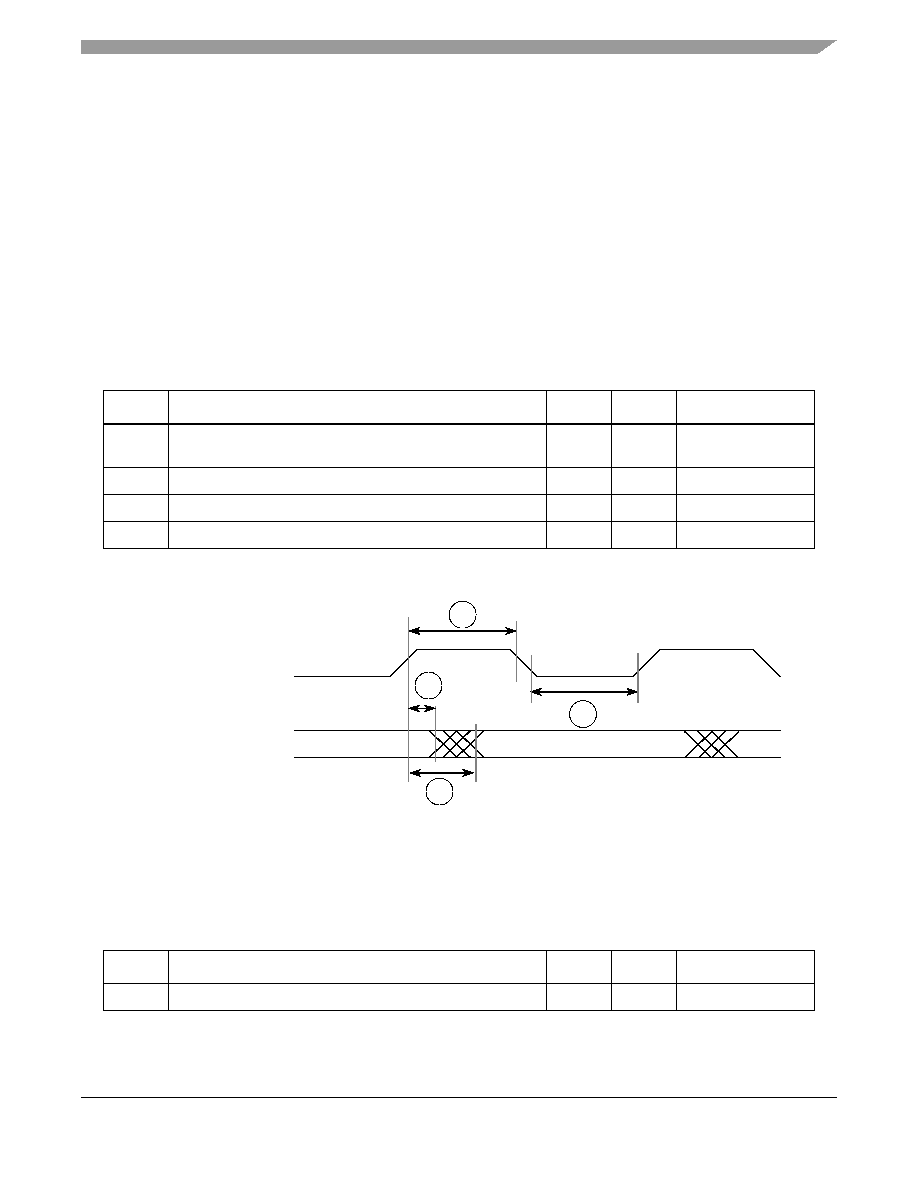
Preliminary Electrical Characteristics
MCF5208 ColdFire
Æ
Microprocessor Data Sheet, Rev. 0.5
Preliminary
Freescale Semiconductor
37
5.11.2 MII Transmit Signal Timing (FEC_TXD[3:0], FEC_TXEN,
FEC_TXER, FEC_TXCLK)
Table 17
lists MII transmit channel timings.
The transmitter functions correctly up to a FEC_TXCLK maximum frequency of 25 MHz +1%. There is
no minimum frequency requirement. In addition, the processor clock frequency must exceed twice the
FEC_TXCLK frequency.
The transmit outputs (FEC_TXD[3:0], FEC_TXEN, FEC_TXER) can be programmed to transition from
either the rising or falling edge of FEC_TXCLK, and the timing is the same in either case. This options
allows the use of non-compliant MII PHYs.
Refer to the Ethernet chapter for details of this option and how to enable it.
Figure 25
shows MII transmit signal timings listed in
Table 17
.
Figure 25. MII Transmit Signal Timing Diagram
5.11.3 MII Async Inputs Signal Timing (FEC_CRS and FEC_COL)
Table 18
lists MII asynchronous inputs signal timing.
Figure 26
shows MII asynchronous input timings listed in
Table 18
.
Table 17. MII Transmit Signal Timing
Num
Characteristic
Min
Max
Unit
M5
FEC_TXCLK to FEC_TXD[3:0], FEC_TXEN, FEC_TXER
invalid
5
--
ns
M6
FEC_TXCLK to FEC_TXD[3:0], FEC_TXEN, FEC_TXER valid
--
25
ns
M7
FEC_TXCLK pulse width high
35%
65%
FEC_TXCLK period
M8
FEC_TXCLK pulse width low
35%
65%
FEC_TXCLK period
Table 18. MII Async Inputs Signal Timing
Num
Characteristic
Min
Max
Unit
M9
FEC_CRS, FEC_COL minimum pulse width
1.5
--
FEC_TXCLK period
M6
FEC_TXCLK (input)
FEC_TXD[3:0] (outputs)
FEC_TXEN
FEC_TXER
M5
M7
M8
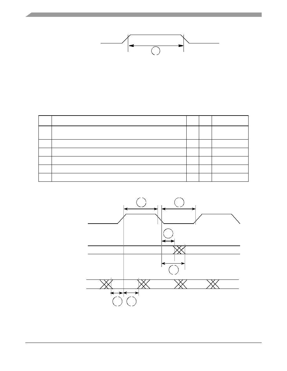
MCF5208 ColdFire
Æ
Microprocessor Data Sheet, Rev. 0.5
Preliminary
Preliminary Electrical Characteristics
Freescale Semiconductor
38
Figure 26. MII Async Inputs Timing Diagram
5.11.4 MII Serial Management Channel Timing (FEC_MDIO and
FEC_MDC)
Table 19
lists MII serial management channel timings. The FEC functions correctly with a maximum
MDC frequency of 2.5 MHz.
Figure 27
shows MII serial management channel timings listed in
Table 19
.
Figure 27. MII Serial Management Channel Timing Diagram
Table 19. MII Serial Management Channel Timing
Num
Characteristic
Min
Max
Unit
M10 FEC_MDC falling edge to FEC_MDIO output invalid (minimum
propagation delay)
0
--
ns
M11 FEC_MDC falling edge to FEC_MDIO output valid (max prop delay)
--
25
ns
M12 FEC_MDIO (input) to FEC_MDC rising edge setup
10
--
ns
M13 FEC_MDIO (input) to FEC_MDC rising edge hold
0
--
ns
M14 FEC_MDC pulse width high
40%
60% FEC_MDC period
M15 FEC_MDC pulse width low
40%
60% FEC_MDC period
FEC_CRS
M9
FEC_COL
M11
FEC_MDC (output)
FEC_MDIO (output)
M12
M13
FEC_MDIO (input)
M10
M14
M15
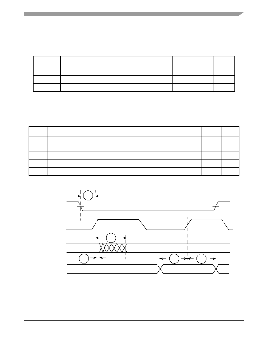
Preliminary Electrical Characteristics
MCF5208 ColdFire
Æ
Microprocessor Data Sheet, Rev. 0.5
Preliminary
Freescale Semiconductor
39
5.12 32-Bit Timer Module AC Timing Specifications
Table 20
lists timer module AC timings.
5.13 QSPI Electrical Specifications
Table 21
lists QSPI timings.
The values in
Table 21
correspond to
Figure 28
.
Figure 28. QSPI Timing
Table 20. Timer Module AC Timing Specifications
Name
Characteristic Unit
Min
Max
T1
DT0IN / DT1IN / DT2IN / DT3IN cycle time
3
--
t
CYC
T2
DT0IN / DT1IN / DT2IN / DT3IN pulse width
1
--
t
CYC
Table 21. QSPI Modules AC Timing Specifications
Name
Characteristic Min
Max
Unit
QS1
QSPI_CS[3:0] to QSPI_CLK
1
510
tcyc
QS2
QSPI_CLK high to QSPI_DOUT valid.
--
10
ns
QS3
QSPI_CLK high to QSPI_DOUT invalid. (Output hold)
1.5
--
ns
QS4
QSPI_DIN to QSPI_CLK (Input setup)
9
--
ns
QS5
QSPI_DIN to QSPI_CLK (Input hold)
9
--
ns
QSPI_CS[3:0]
QSPI_CLK
QSPI_DOUT
QS5
QS1
QSPI_DIN
QS3
QS4
QS2
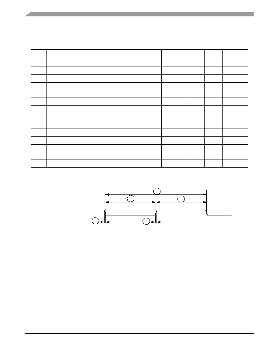
MCF5208 ColdFire
Æ
Microprocessor Data Sheet, Rev. 0.5
Preliminary
Preliminary Electrical Characteristics
Freescale Semiconductor
40
5.14 JTAG and Boundary Scan Timing
Figure 29. Test Clock Input Timing
Table 22. JTAG and Boundary Scan Timing
Num
Characteristics
1
NOTES:
1
JTAG_EN is expected to be a static signal. Hence, specific timing is not associated with it.
Symbol
Min
Max
Unit
J1
TCLK Frequency of Operation
f
JCYC
DC
1/4
f
sys/2
J2
TCLK Cycle Period
t
JCYC
4
--
t
CYC
J3
TCLK Clock Pulse Width
t
JCW
26
--
ns
J4
TCLK Rise and Fall Times
t
JCRF
0
3
ns
J5
Boundary Scan Input Data Setup Time to TCLK Rise
t
BSDST
4
--
ns
J6
Boundary Scan Input Data Hold Time after TCLK Rise
t
BSDHT
26
--
ns
J7
TCLK Low to Boundary Scan Output Data Valid
t
BSDV
0
33
ns
J8
TCLK Low to Boundary Scan Output High Z
t
BSDZ
0
33
ns
J9
TMS, TDI Input Data Setup Time to TCLK Rise
t
TAPBST
4
--
ns
J10
TMS, TDI Input Data Hold Time after TCLK Rise
t
TAPBHT
10
--
ns
J11
TCLK Low to TDO Data Valid
t
TDODV
0
26
ns
J12
TCLK Low to TDO High Z
t
TDODZ
0
8
ns
J13
TRST Assert Time
t
TRSTAT
100
--
ns
J14
TRST Setup Time (Negation) to TCLK High
t
TRSTST
10
--
ns
TCLK
V
IL
V
IH
J3
J3
J4
J4
J2
(input)
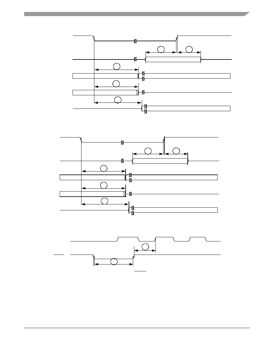
Preliminary Electrical Characteristics
MCF5208 ColdFire
Æ
Microprocessor Data Sheet, Rev. 0.5
Preliminary
Freescale Semiconductor
41
Figure 30. Boundary Scan (JTAG) Timing
Figure 31. Test Access Port Timing
Figure 32. TRST Timing
5.15 Debug AC Timing Specifications
Table 23
lists specifications for the debug AC timing parameters shown in
Figure 33
&
Figure 34
.
Input Data Valid
Output Data Valid
Output Data Valid
TCLK
Data Inputs
Data Outputs
Data Outputs
Data Outputs
V
IL
V
IH
J5
J6
J7
J8
J7
Input Data Valid
Output Data Valid
Output Data Valid
TCLK
TDI
TDO
TDO
TDO
TMS
V
IL
V
IH
J9
J10
J11
J12
J11
TCLK
TRST
J14
J13
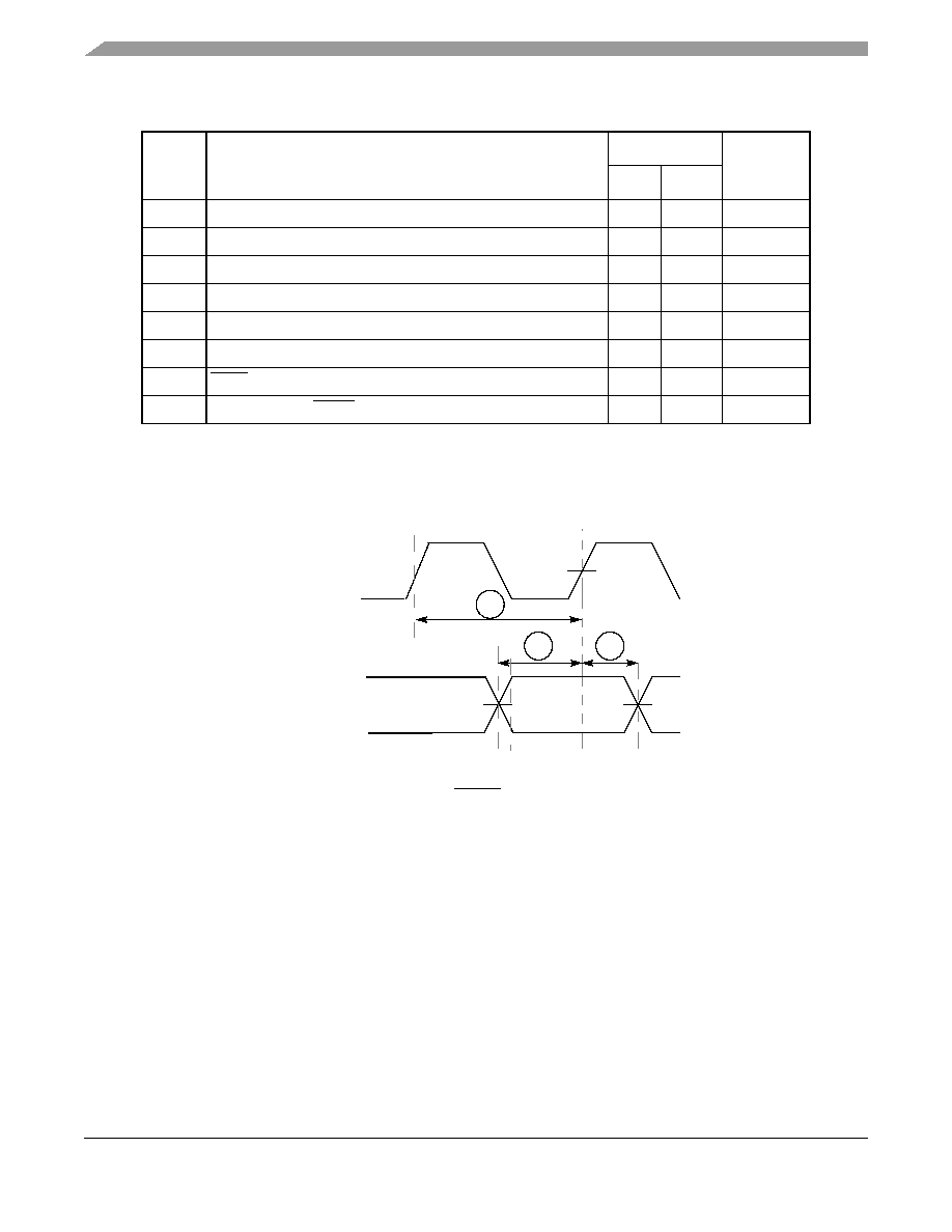
MCF5208 ColdFire
Æ
Microprocessor Data Sheet, Rev. 0.5
Preliminary
Preliminary Electrical Characteristics
Freescale Semiconductor
42
Figure 33
shows real-time trace timing for the values in
Table 23
.
Figure 33. Real-Time Trace AC Timing
Figure 34
shows BDM serial port AC timing and BKPT pin timing for the values in
Table 23
.
Table 23. Debug AC Timing Specification
Num
Characteristic
Units
Min
Max
DE0
PSTCLK cycle time
--
0.5
t
cyc
DE1
PST valid to PSTCLK high
2
--
ns
DE2
PSTCLK high to PST invalid
1
--
ns
DE3
DSCLK cycle time
5
--
t
cyc
DE4
DSI valid to DSCLK high
1
--
t
cyc
DE5
1
NOTES:
1
DSCLK and DSI are synchronized internally. DE4 is measured from the synchronized DSCLK input
relative to the rising edge of FB_CLK.
DSCLK high to DSO invalid
4
--
t
cyc
DE6
BKPT input data setup time to FB_CLK high
4
--
ns
DE7
FB_CLK high to BKPT invalid
0 --
ns
PSTCLK
PST[3:0]
DE2
DE1
DDATA[3:0]
DE0
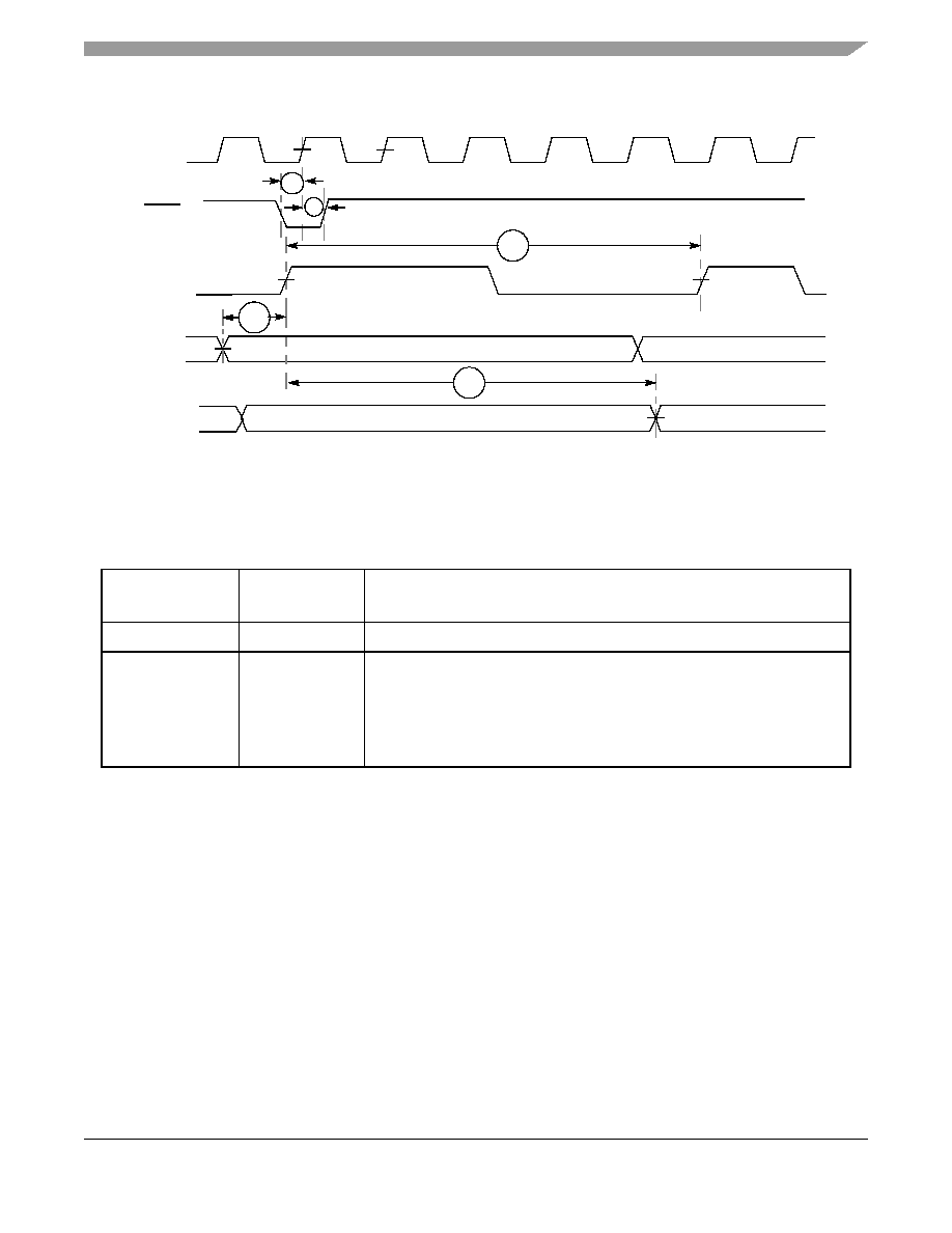
Revision History
MCF5208 ColdFire
Æ
Microprocessor Data Sheet, Rev. 0.5
Preliminary
Freescale Semiconductor
43
Figure 34. BDM Serial Port AC Timing
6
Revision History
Table 24. Revision History
Revision
Number
Date
Substantive Changes
0
5/23/2005
∑ Initial Release
0.1
6/16/2005
∑ Corrected 144QFP pinout in
Figure 1
. Pins 139-142 incorrectly showed
FEC functionality, which are actually UART 0/1 clear-to-send and
request-to-send signals.
∑ Changed maximum core frequency in
Table 8
, spec #2, from 240MHz to
166.67MHz. Also, changed symbols in table: f
core
-> f
sys
and f
sys
-> f
sys/2
for consistency throughout document and reference manual.
DSI
DSO
Current
Next
FB_CLK
Past
Current
DSCLK
DE3
BKPT
DE6
DE7
DE4
DE5
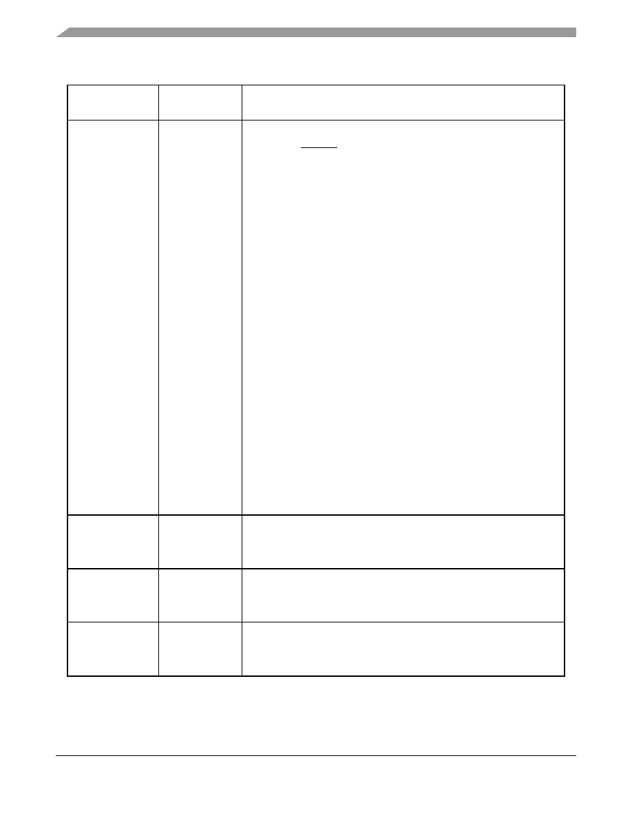
MCF5208 ColdFire
Æ
Microprocessor Data Sheet, Rev. 0.5
Preliminary
Revision History
Freescale Semiconductor
44
0.2
8/26/2005
∑ Changed ball M9 from SD_VDD to EVDD in
Figure 9
.
∑
Table 3
: Pin 33 for 144 LQFP package should be EVDD instead of
SD_VDD. BE/BWE[3:0] for 144 LQFP should be "20, 48, 18, 50" instead
of "18, 20, 48, 50"
Cleaned up various electrical specifications:
∑
Table 4
: Added DDR/Memory pad supply voltage spec, changed "clock
synthesizer supply voltage" to "PLL supply voltage", changed min PLLV
DD
from -0.5 to -0.3, changed max V
IN
from 4.0 to 3.6, changed minimum T
stg
from -65 to -55,
∑
Table 5
: Changed TBD values in T
j
entry to 105
∞C.
∑
Table 7
: Changed minimum core supply voltage from 1.35 to 1.4 and
maximum from 1.65 to 1.6, added PLL supply voltage entry, added pad
supply entries for mobile-DDR, DDR, and SDR, changed minimum input
high voltage from 0.7xEV
DD
to 2 and maximum from 3.65 to EV
DD
+0.05,
changed minimum input low voltage from VSS-0.3 to -0.05 and maximum
from 0.35xEV
DD
to 0.8, added input high/low voltage entries for DDR and
mobile-DDR, removed high impedance leakage current entry, changed
minimum output high voltage from EV
DD
-0.5 to EV
DD
-0.4, added DDR/bus
output high/low voltage entries, removed load capacitance and DC
injection current entries.
∑ Added filtering circuits and voltage sequencing sections:
Section 5.4.1,
"PLL Power Filtering,"
and
Section 5.4.2, "Supply Voltage Sequencing and
Separation Cautions."
∑ Removed "Operating Conditions" table from
Section 5.5, "Oscillator and
PLL Electrical Characteristics,"
since it is redundant with
Table 7
.
∑
Table 9
: Changed minimum core frequency to TBD, removed external
reference and on-chip PLL frequency specs to have only a CLKOUT
frequency spec of TBD to 83.33MHz, removed loss of reference frequency
and self-clocked mode frequency entries, in EXTAL input high/low voltage
entries changed "All other modes (Dual controller (1:1), Bypass, External)"
to "All other modes (External, Limp)", removed XTAL output high/low
voltage entries, removed power-up to lock time entry, removed last 5
entries (frequency un-lock range, frequency lock range, CLKOUT period
jitter, frequency modulation range limit, and ICO frequency)
0.3
9/07/2005
∑ Corrected DRAMSEL footnote #3 in
Table 3
.
∑ Updated
Table 3
with 144MAPBGA pin locations.
∑ Added 144MAPBGA ballmap to
Section 4.3, "Pinout--144 MAPBGA."
∑ Changed J12 from PLL_VDD to IVDD in
Figure 9
.
0.4
10/10/2005
∑
Figure 1
and
Table 3
: Changed pin 33 from EVDD to SD_VDD
∑
Figure 4
and
Table 3
: Changed ball D10 from TEST to VSS
∑
Figure 6
and
Table 3
: Changed pin 39 from EVDD to SD_VDD and pin 117
from TEST to VSS
0.5
3/29/2006
∑ Added "top view" and "bottom view" labels where appropriate to
mechanical drawings and pinouts.
∑ Updated mechanical drawings to latest available, and added note to
Section 4, "Mechanicals and Pinouts."
Table 24. Revision History (continued)
Revision
Number
Date
Substantive Changes

THIS PAGE INTENTIONALLY LEFT BLANK
MCF5208 ColdFire
Æ
Microprocessor Data Sheet, Rev. 0.5
Preliminary
Freescale Semiconductor
45

How to Reach Us:
Home Page:
www.freescale.com
E-mail:
support@freescale.com
USA/Europe or Locations Not Listed:
Freescale Semiconductor
Technical Information Center, CH370
1300 N. Alma School Road
Chandler, Arizona 85224
+1-800-521-6274 or +1-480-768-2130
support@freescale.com
Europe, Middle East, and Africa:
Freescale Halbleiter Deutschland GmbH
Technical Information Center
Schatzbogen 7
81829 Muenchen, Germany
+44 1296 380 456 (English)
+46 8 52200080 (English)
+49 89 92103 559 (German)
+33 1 69 35 48 48 (French)
support@freescale.com
Japan:
Freescale Semiconductor Japan Ltd.
Headquarters
ARCO Tower 15F
1-8-1, Shimo-Meguro, Meguro-ku,
Tokyo 153-0064, Japan
0120 191014 or +81 3 5437 9125
support.japan@freescale.com
Asia/Pacific:
Freescale Semiconductor Hong Kong Ltd.
Technical Information Center
2 Dai King Street
Tai Po Industrial Estate
Tai Po, N.T., Hong Kong
+800 2666 8080
support.asia@freescale.com
For Literature Requests Only:
Freescale Semiconductor Literature Distribution Center
P.O. Box 5405
Denver, Colorado 80217
1-800-441-2447 or 303-675-2140
Fax: 303-675-2150
LDCForFreescaleSemiconductor@hibbertgroup.com
Information in this document is provided solely to enable system and
software implementers to use Freescale Semiconductor products. There are
no express or implied copyright licenses granted hereunder to design or
fabricate any integrated circuits or integrated circuits based on the
information in this document.
Freescale Semiconductor reserves the right to make changes without further
notice to any products herein. Freescale Semiconductor makes no warranty,
representation or guarantee regarding the suitability of its products for any
particular purpose, nor does Freescale Semiconductor assume any liability
arising out of the application or use of any product or circuit, and specifically
disclaims any and all liability, including without limitation consequential or
incidental damages. "Typical" parameters that may be provided in Freescale
Semiconductor data sheets and/or specifications can and do vary in different
applications and actual performance may vary over time. All operating
parameters, including "Typicals", must be validated for each customer
application by customer's technical experts. Freescale Semiconductor does
not convey any license under its patent rights nor the rights of others.
Freescale Semiconductor products are not designed, intended, or authorized
for use as components in systems intended for surgical implant into the body,
or other applications intended to support or sustain life, or for any other
application in which the failure of the Freescale Semiconductor product could
create a situation where personal injury or death may occur. Should Buyer
purchase or use Freescale Semiconductor products for any such unintended
or unauthorized application, Buyer shall indemnify and hold Freescale
Semiconductor and its officers, employees, subsidiaries, affiliates, and
distributors harmless against all claims, costs, damages, and expenses, and
reasonable attorney fees arising out of, directly or indirectly, any claim of
personal injury or death associated with such unintended or unauthorized
use, even if such claim alleges that Freescale Semiconductor was negligent
regarding the design or manufacture of the part.
FreescaleTM and the Freescale logo are trademarks of Freescale
Semiconductor, Inc. All other product or service names are the property
of their respective owners.© Freescale Semiconductor, Inc. 2006. All rights
reserved.
MCF5208EC
Rev. 0.5
3/2006