 | –≠–ª–µ–∫—Ç—Ä–æ–Ω–Ω—ã–π –∫–æ–º–ø–æ–Ω–µ–Ω—Ç: MCF5235 | –°–∫–∞—á–∞—Ç—å:  PDF PDF  ZIP ZIP |

© Freescale Semiconductor, Inc., 2004. All rights reserved.
∑ Preliminary
Freescale Semiconductor
Hardware Specification
MCF5235EC
Rev. 1.3, 10/2004
Technical Data
Table of Contents
The MCF523x is a family of highly-integrated 32-bit
microcontrollers based on the V2 ColdFire
microarchitecture. Featuring a 16 or 32 channel eTPU,
64 Kbytes of internal SRAM, a 2-bank SDRAM
controller, four 32-bit timers with dedicated DMA, a 4
channel DMA controller, up to 2 CAN modules, 3
UARTs and a queued SPI, the MCF523x family has been
designed for general purpose industrial control
applications. It is also a high-performance upgrade for
users of the MC68332. This document provides an
overview of the MCF523x microcontroller family, as
well as detailed descriptions of the mechanical and
electrical characteristics of the devices.
The MCF523x family is based on the Version 2 ColdFire
reduced instruction set computing (RISC)
microarchitecture operating at a core frequency of up to
150 MHz and bus frequency up to 75 MHz.
1
Overview
This 32-bit device's on-chip modules include:
1
Overview ......................................................... 1
2
Signal Descriptions.......................................... 9
3
Modes of Operation ....................................... 14
4
Design Recommendations ............................ 17
5
Mechanicals/Pinouts and Part Numbers ....... 25
6
Preliminary Electrical Characteristics ............ 34
7
Documentation .............................................. 58
MCF523x Integrated
Microprocessor
Hardware Specification
32-bit Embedded Controller Division
MCF523x Integrated Microprocessor Hardware Specification, Rev. 1.3
Preliminary
Overview
Freescale Semiconductor
2
∑
V2 ColdFire core with enhanced multiply-accumulate unit (EMAC) providing 144 Dhrystone 2.1
MIPS @ 150 MHz
∑
eTPU with 16 or 32 channels, 6 Kbytes of code memory and 1.5 Kbytes of data memory with
Nexus Class 1 debug support
∑
64 Kbytes of internal SRAM
∑
External bus speed of one half the CPU operating frequencey (75 MHz bus @ 150 MHz core)
∑
10/100 Mbps bus-mastering Ethernet controller
∑
8 Kbytes of configurable instruction/data cache
∑
Three universal asynchronous receiver/transmitters (UARTs)
∑
Controller area network 2.0B (FlexCAN) module
-- Optional second FlexCAN module multiplexed with the third UART
∑
Inter-integrated circuit (I
2
CTM) bus controller
∑
Queued serial peripheral interface (QSPI) module
∑
Hardware cryptography accelerator (optional)
-- Random number generator
-- DES/3DES/AES block cipher engine
-- MD5/SHA-1/HMAC accelerator
∑
Four channel 32-bit direct memory access (DMA) controller
∑
Four channel 32-bit input capture/output compare timers with optional DMA support
∑
Four channel 16-bit periodic interrupt timers (PITs)
∑
Programmable software watchdog timer
∑
Interrupt controller capable of handling up to 126 interrupt sources
∑
Clock module with integrated phase locked loop (PLL)
∑
External bus interface module including a 2-bank synchronous DRAM controller
∑
32-bit non-multiplexed bus with up to 8 chip select signals that support paged mode Flash
memories
1.1
MCF523x Family Configurations
Table 1. MCF523x Family Configurations
Module
5232
5233
5234
5235
ColdFire V2 Core with EMAC
(Enhanced Multiply-Accumulate
Unit)
x
x
x
x
Enhanced Time Processor Unit
with memory (eTPU)
16-ch
6K
32-ch
6K
16-ch
6K
32-ch
6K
System Clock
up to 150 MHz
Performance (Dhrystone/2.1 MIPS)
up to 144
Overview
MCF523x Integrated Microprocessor Hardware Specification, Rev. 1.3
Preliminary
Freescale Semiconductor
3
1.2
Block Diagram
The superset device in the MCF523x family comes in a 256 mold array process ball grid array (MAPBGA)
package.
Figure 1
shows a top-level block diagram of the MCF5235, the superset device.
Instruction/Data Cache
8 Kbytes
Static RAM (SRAM)
64 Kbytes
Interrupt Controllers (INTC)
2
2
2
2
Edge Port Module (EPORT)
x
x
x
x
External Interface Module (EIM)
x
x
x
x
4-channel Direct-Memory Access
(DMA)
x
x
x
x
SDRAM Controller
x
x
x
x
Fast Ethernet Controller (FEC)
--
--
x
x
Cryptography - Security module for
data packets processing
--
--
--
x
Watchdog Timer (WDT)
x
x
x
x
Four Periodic Interrupt Timers (PIT)
x
x
x
x
32-bit DMA Timers
4
4
4
4
QSPI
x
x
x
x
UART(s)
3
3
3
3
I
2
C
x
x
x
x
FlexCAN 2.0B - Controller-Area
Network communication module
1
2
1
2
General Purpose I/O Module
(GPIO)
x
x
x
x
JTAG - IEEE 1149.1 Test Access
Port
x
x
x
x
Package
160 QFP
196
MAPBGA
256
MAPBGA
256
MAPBGA
256
MAPBGA
Table 1. MCF523x Family Configurations (continued)
Module
5232
5233
5234
5235
MCF523x Integrated Microprocessor Hardware Specification, Rev. 1.3
Preliminary
Overview
Freescale Semiconductor
4
Figure 1. MCF5235 Block Diagram
64 Kbytes
SRAM
(8Kx16)x4
FlexCAN
eTPU
EIM
ETHERNET
V2 ColdFire CPU
INTC0
Watchdog
PIT0
JTAG
TAP
CACHE
(1Kx32)x2
PIT1
PIT2
PIT3
4 CH DMA
UART
0
UART
1
I
2
C
QSPI
DTIM
0
DTIM
1
DTIM
2
DTIM
3
Timer
P
A
DI ≠
P
i
n Muxin
g
PLL
CLKGEN
UART
2
8 Kbytes
Edge
Port
SDRAMC
CHIP
EBI
SELECTS
(To/From PADI)
(To/From
eTPU
CANTX
CANRX
FAST
CONTROLLER
(FEC)
FEC
DTnIN
DTnOUT
UnRXD
UnTXD
I2C_SDA
I2C_SCL
SDRAMC
QSPI
UnRTS
UnCTS
PORTS
CIM
(To/From PADI)
NEXUS
(GPIO)
D[31:0]
A[23:0]
R/W
CS[3:0]
TA
TSIZ[1:0]
TEA
BS[3:0]
DIV
EMAC
DREQ[2:0]
INTC1
Arbiter
(To/From SRAM backdoor)
(To/From Arbiter backdoor)
SKHA
RNGA
MDHA
(To/From PADI)
Cryptography
Modules
(x2)
DACK[2:0]
BDM
(To/From INTC)
MU
X
PADI)
JTAG_EN

Overview
MCF523x Integrated Microprocessor Hardware Specification, Rev. 1.3
Preliminary
Freescale Semiconductor
5
1.3
Features
The following section gives a brief overview of this family's feature set. For more detailed information see
the MCF5235 Reference Manual (MCF5235RM).
1.3.1
Feature Overview
∑
Version 2 ColdFire variable-length RISC processor core
-- Static operation
-- 32-bit address and data path on-chip
-- Processor core runs at twice the bus frequency
-- Sixteen general-purpose 32-bit data and address registers
-- Implements the ColdFire Instruction Set Architecture, ISA_A+, with extensions to support the
user stack pointer register, and 4 new instructions for improved bit processing
-- Enhanced Multiply-Accumulate (EMAC) unit with four 48-bit accumulators to support 32-bit
signal processing algorithms
-- Illegal instruction decode that allows for 68K emulation support
∑
Enhanced Time Processor Unit (eTPU)
-- Event triggered VLIW processor timer subsystem
-- 32 channels
-- 24-bit timer resolution
-- 6 Kbyte of code memory and 1.5 Kbyte of data memory
-- Variable number of parameters allocatable per channel
-- Double match/capture channels
-- Angle mode support
-- DMA and interrupt request support
-- Nexus Class 1 Debug support
∑
System debug support
-- Integrated debug supports both ColdFire Debug and Nexus class 1 features on a single port
with cross triggering operations for ease of use
-- Unified programming model including both ColdFire and Nexus debug registers
-- Real time trace for determining dynamic execution path
-- Background debug mode (BDM) for in-circuit debugging
-- Real time debug support, with two user-visible hardware breakpoint registers (PC and address
with optional data) that can be configured into a 1- or 2-level trigger
∑
On-chip memories
-- 8-Kbyte cache, configurable as instruction-only, data-only, or split I-/D-cache
-- 64-Kbyte dual-ported SRAM on CPU internal bus, accessible by core and non-core bus

MCF523x Integrated Microprocessor Hardware Specification, Rev. 1.3
Preliminary
Overview
Freescale Semiconductor
6
masters (e.g., DMA, FEC)
∑
Fast Ethernet Controller (FEC)
-- 10 BaseT capability, half duplex or full duplex
-- 100 BaseT capability, half duplex or full duplex
-- On-chip transmit and receive FIFOs
-- Built-in dedicated DMA controller
-- Memory-based flexible descriptor rings
-- Media independent interface (MII) to external transceiver (PHY)
∑
FlexCAN Modules (up to 2)
-- Full implementation of the CAN protocol specification version 2.0B
≠ Standard Data and Remote Frames (up to 109 bits long)
≠ Extended Data and Remote Frames (up to 127 bits long)
≠ 0≠8 bytes data length
≠ Programmable bit rate up to 1 Mbit/sec
-- Flexible Message Buffers (MBs), totalling up to 16 message buffers of 0≠8 bytes data length
each, configurable as Rx or Tx, all supporting standard and extended messages
-- Unused MB space can be used as general purpose RAM space
-- Listen only mode capability
-- Content-related addressing
-- Three programmable mask registers: global (for MBs 0-13), special for MB14 and special for
MB15
-- Programmable transmit-first scheme: lowest ID or lowest buffer number
-- "Time stamp" based on 16-bit free-running timer
-- Global network time, synchronized by a specific message
∑
Three Universal Asynchronous Receiver Transmitters (UARTs)
-- 16-bit divider for clock generation
-- Interrupt control logic
-- Maskable interrupts
-- DMA support
-- Data formats can be 5, 6, 7 or 8 bits with even, odd or no parity
-- Up to 2 stop bits in 1/16 increments
-- Error-detection capabilities
-- Modem support includes request-to-send (UnRTS) and clear-to-send (UnCTS) lines
-- Transmit and receive FIFO buffers
∑
I
2
C Module
-- Interchip bus interface for EEPROMs, LCD controllers, A/D converters, and keypads

Overview
MCF523x Integrated Microprocessor Hardware Specification, Rev. 1.3
Preliminary
Freescale Semiconductor
7
-- Fully compatible with industry-standard I
2
C bus
-- Master or slave modes support multiple masters
-- Automatic interrupt generation with programmable level
∑
Queued Serial Peripheral Interface (QSPI)
-- Full-duplex, three-wire synchronous transfers
-- Up to four chip selects available
-- Master mode operation only
-- Programmable master bit rates
-- Up to 16 pre-programmed transfers
∑
Four 32-bit DMA Timers
-- 13-ns resolution at 75 MHz
-- Programmable sources for clock input, including an external clock option
-- Programmable prescaler
-- Input-capture capability with programmable trigger edge on input pin
-- Output-compare with programmable mode for the output pin
-- Free run and restart modes
-- Maskable interrupts on input capture or reference-compare
-- DMA trigger capability on input capture or reference-compare
∑
Four Periodic Interrupt Timers (PITs)
-- 16-bit counter
-- Selectable as free running or count down
∑
Software Watchdog Timer
-- 16-bit counter
-- Low power mode support
∑
Phase Locked Loop (PLL)
-- Crystal or external oscillator reference
-- 8 to 25 MHz reference frequency for normal PLL mode
-- 24 to 75 MHz oscillator reference frequency for 2:1 mode
-- Separate clock output pin
∑
Interrupt Controllers (x2)
-- Support for up to 110 interrupt sources organized as follows:
≠ 103 fully-programmable interrupt sources
≠ 7 fixed-level external interrupt sources
-- Unique vector number for each interrupt source
-- Ability to mask any individual interrupt source or all interrupt sources (global mask-all)

MCF523x Integrated Microprocessor Hardware Specification, Rev. 1.3
Preliminary
Overview
Freescale Semiconductor
8
-- Support for hardware and software interrupt acknowledge (IACK) cycles
-- Combinatorial path to provide wake-up from low power modes
∑
DMA Controller
-- Four fully programmable channels
-- Dual-address and single-address transfer support with 8-, 16- and 32-bit data capability along
with support for 16-byte (4
◊ 32-bit) burst transfers
-- Source/destination address pointers that can increment or remain constant
-- 24-bit byte transfer counter per channel
-- Auto-alignment transfers supported for efficient block movement
-- Bursting and cycle steal support
-- Software-programmable connections between the 12 DMA requesters in the UARTs (3),
32-bit timers (4) plus external logic (4) the four DMA channels and the eTPU (1)
∑
External Bus Interface
-- Glueless connections to external memory devices (e.g., SRAM, Flash, ROM, etc.)
-- SDRAM controller supports 8-, 16-, and 32-bit wide memory devices
-- Support for n-1-1-1 burst fetches from page mode Flash
-- Glueless interface to SRAM devices with or without byte strobe inputs
-- Programmable wait state generator
-- 32-bit bidirectional data bus
-- 24-bit address bus
-- Up to eight chip selects available
-- Byte/write enables (byte strobes)
-- Ability to boot from external memories that are 8, 16, or 32 bits wide
∑
Chip Integration Module (CIM)
-- System configuration during reset
-- Selects one of four clock modes
-- Sets boot device and its data port width
-- Configures output pad drive strength
-- Unique part identification number and part revision number
-- Reset
≠ Separate reset in and reset out signals
≠ Six sources of reset: Power-on reset (POR), External, Software, Watchdog, PLL loss of
clock, PLL loss of lock
≠ Status flag indication of source of last reset
∑
General Purpose I/O interface
-- Up to 142 bits of general purpose I/O
Signal Descriptions
MCF523x Integrated Microprocessor Hardware Specification, Rev. 1.3
Preliminary
Freescale Semiconductor
9
-- Bit manipulation supported via set/clear functions
-- Unused peripheral pins may be used as extra GPIO
∑
JTAG support for system level board testing
2
Signal Descriptions
This section describes signals that connect off chip, including a table of signal properties. For a more
detailed discussion of the MCF523x signals, consult the MCF5235 Reference Manual (MCF5235RM).
2.1
Signal Properties
Table 2
lists all of the signals grouped by function. The "Dir" column is the direction for the primary
function of the pin. Refer to
Section 5, "Mechanicals/Pinouts and Part Numbers
," for package diagrams.
NOTE
In this table and throughout this document a single signal within a group is
designated without square brackets (i.e., A24), while designations for
multiple signals within a group use brackets (i.e., A[23:21]) and is meant to
include all signals within the two bracketed numbers when these numbers
are separated by a colon.
NOTE
The primary functionality of a pin is not necessarily its default functionality.
Pins that are muxed with GPIO will default to their GPIO functionality.
Table 2. MCF523x Signal Information and Muxing
Signal Name
GPIO
Alternate 1 Alternate 2
Dir.
1
MCF5232
160
QFP
MCF5232
196
MAPBGA
MCF5233
256
MAPBGA
MCF5234
256
MAPBGA
MCF5235
256
MAPBGA
Reset
RESET
--
--
--
I
83
N13
T15
T15
T15
RSTOUT
--
--
--
O
82
P13
T14
T14
T14
Clock
EXTAL
--
--
--
I
86
M14
P16
P16
P16
XTAL
--
--
--
O
85
N14
R16
R16
R16
CLKOUT
--
--
--
O
89
K14
M16
M16
M16
Mode Selection
CLKMOD[1:0]
--
--
--
I
19,20
G5, H5
J3, J2
J3, J2
J3, J2
RCON
--
--
--
I
79
K10
P13
P13
P13
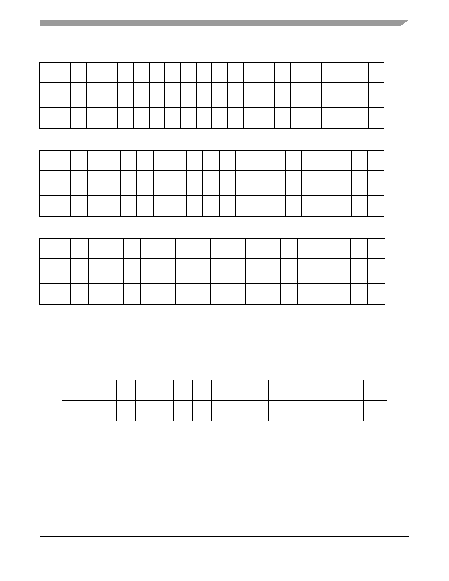
External Memory Interface and Ports
MCF523x Integrated Microprocessor Hardware Specification, Rev. 1.3
Preliminary
Signal Descriptions
Freescale Semiconductor
10
A[23:21]
PADDR[7:5]
CS[6:4]
--
O
126, 125,
124
B11, C11,
D11
B14, C14,
A15
B14, C14,
A15
B14, C14,
A15
A[20:0]
--
--
--
O
123:115,
112:106,
102:98
A12, B12,
C12, A13,
B13, B14,
C13, C14,
D12, D13,
D14, E11,
E12, E13,
E14, F12,
F13, F14,
G11, G12,
G13
B15, B16,
C15, C16,
D16, D15,
D14, E16,
E15, E14,
E13, F15,
F14, F13,
G15, G14,
G13, H16,
H15, H14,
H13
B15, B16,
C15, C16,
D16, D15,
D14, E16,
E15, E14,
E13, F15,
F14, F13,
G15, G14,
G13, H16,
H15, H14,
H13
B15, B16,
C15, C16,
D16, D15,
D14, E16,
E15, E14,
E13, F15,
F14, F13,
G15, G14,
G13, H16,
H15, H14,
H13
D[31:16]
--
--
--
O
21:24, 26:30,
33:39
G1, G2, H1,
H2, H3, H4,
J1, J2, J3,
J4, K1, K2,
K3, K4, L1,
L2
K4, K3, K2,
K1, L4, L3,
L2, L1, M3,
M2, M1,
N2, N1, P2,
P1, R1
K4, K3, K2,
K1, L4, L3,
L2, L1, M3,
M2, M1,
N2, N1, P2,
P1, R1
K4, K3, K2,
K1, L4, L3,
L2, L1, M3,
M2, M1,
N2, N1, P2,
P1, R1
D[15:8]
PDATAH[7:0]
--
--
O
42:49,
M1, N1, M2,
N2, P2, L3,
M3, N3,
R2, T2, N3,
P3, R3, T3,
N4, P4,
R2, T2, N3,
P3, R3, T3,
N4, P4,
R2, T2, N3,
P3, R3, T3,
N4, P4,
D[7:0]
PDATAL[7:0]
--
--
O
50:52, 56:60 P3, M4, N4,
P4, L5, M5,
N5, P5
R4, T4, P5,
R5, N6, P6,
R6, N7
R4, T4, P5,
R5, N6, P6,
R6, N7
R4, T4, P5,
R5, N6, P6,
R6, N7
BS[3:0]
PBS[7:4]
CAS[3:0]
--
O
143:140
B6, C6, D7,
C7
C9, B9, A9,
A10
C9, B9, A9,
A10
C9, B9, A9,
A10
OE
PBUSCTL7
--
--
O
63
N6
T7
T7
T7
TA
PBUSCTL6
--
--
I
97
H11
K14
K14
K14
TEA
PBUSCTL5
DREQ1
--
I
--
J14
K13
K13
K13
R/W
PBUSCTL4
--
--
O
96
J13
L16
L16
L16
TSIZ1
PBUSCTL3
DACK1
--
O
--
P6
N8
N8
N8
TSIZ0
PBUSCTL2
DACK0
--
O
--
P7
P8
P8
P8
TS
PBUSCTL1
DACK2
--
O
--
H13
K16
K16
K16
TIP
PBUSCTL0
DREQ0
--
O
--
H12
K15
K15
K15
Chip Selects
CS[7:4]
PCS[7:4]
--
--
O
--
B9, A10,
C10, A11
C12, A13,
C13, A14
C12, A13,
C13, A14
C12, A13,
C13, A14
CS[3:2]
PCS[3:2]
SD_CS[1:0]
--
O
134,133
A9, C9
B12, D12
B12, D12
B12, D12
CS1
PCS1
--
--
O
130
B10
B13
B13
B13
CS0
--
--
--
O
129
D10
D13
D13
D13
Table 2. MCF523x Signal Information and Muxing (continued)
Signal Name
GPIO
Alternate 1 Alternate 2
Dir.
1
MCF5232
160
QFP
MCF5232
196
MAPBGA
MCF5233
256
MAPBGA
MCF5234
256
MAPBGA
MCF5235
256
MAPBGA
Signal Descriptions
MCF523x Integrated Microprocessor Hardware Specification, Rev. 1.3
Preliminary
Freescale Semiconductor
11
SDRAM Controller
SD_WE
PSDRAM5
--
--
O
93
K13
L13
L13
L13
SD_SCAS
PSDRAM4
--
--
O
92
K12
M15
M15
M15
SD_SRAS
PSDRAM3
--
--
O
91
K11
M14
M14
M14
SD_CKE
PSDRAM2
--
--
O
139
E8
C10
C10
C10
SD_CS[1:0]
PSDRAM[1:0]
--
--
O
--
L12, L13
N15, M13
N15, M13
N15, M13
External Interrupts Port
IRQ[7:3]
PIRQ[7:3]
--
--
I
IRQ7=64
IRQ4=65
N7, M7, L7,
P8, N8
R8, T8, N9,
P9, R9
R8, T8, N9,
P9, R9
R8, T8, N9,
P9, R9
IRQ2
PIRQ2
DREQ2
--
I
--
M8
T9
T9
T9
IRQ1
PIRQ1
--
--
I
66
L8
N10
N10
N10
eTPU
TPUCH31
--
ECOL
--
--
--
F3
--
F3
TPUCH30
--
ECRS
--
--
--
F4
--
F4
TPUCH29
--
ERXCLK
--
--
--
E3
--
E3
TPUCH28
--
ERXDV
--
--
--
E4
--
E4
TPUCH[27:24]
--
ERXD[3:0]
--
--
--
D3, D4, C3,
C4
--
D3, D4, C3,
C4
TPUCH23
--
ERXER
--
--
--
D5
--
D5
TPUCH22
--
ETXCLK
--
--
--
C5
--
C5
TPUCH21
--
ETXEN
--
--
--
D6
--
D6
TPUCH20
--
ETXER
--
--
--
C6
--
C6
TPUCH[19:16]
--
ETXD[3:0]
--
--
--
B6,B5, A5,
B7
--
B6,B5, A5,
B7
TPUCH[15:0]
--
--
--
11, 10, 7:2,
159:154,
152, 151
E2, E1, D1
D2, D3, C1,
C2, B1, B2,
A2, C3, B3,
A3, A4, C4,
BR
F2, E1, E2,
D1, D2, C1,
C2, B1, B2,
A2, B3, A3,
B4, A4, A6,
A7
F2, E1, E2,
D1, D2, C1,
C2, B1, B2,
A2, B3, A3,
B4, A4, A6,
A7
F2, E1, E2,
D1, D2, C1,
C2, B1, B2,
A2, B3, A3,
B4, A4, A6,
A7
TCRCLK
PETPU2
--
--
12
E3
F1
F1
F1
UTPUODIS
PETPU1
--
--
--
H10
J13
J13
J13
LTPUODIS
PETPU0
--
--
--
G10
J14
J14
J14
FEC
EMDIO
PFECI2C2
I2C_SDA
U2RXD
I/O
--
--
--
C7
C7
Table 2. MCF523x Signal Information and Muxing (continued)
Signal Name
GPIO
Alternate 1 Alternate 2
Dir.
1
MCF5232
160
QFP
MCF5232
196
MAPBGA
MCF5233
256
MAPBGA
MCF5234
256
MAPBGA
MCF5235
256
MAPBGA
MCF523x Integrated Microprocessor Hardware Specification, Rev. 1.3
Preliminary
Signal Descriptions
Freescale Semiconductor
12
EMDC
PFECI2C3
I2C_SCL
U2TXD
O
--
--
--
D7
D7
ECOL
--
--
--
I
--
--
--
F3
F3
ECRS
--
--
--
I
--
--
--
F4
F4
ERXCLK
--
--
--
I
--
--
--
E3
E3
ERXDV
--
--
--
I
--
--
--
E4
E4
ERXD[3:0]
--
--
--
I
--
--
--
D3, D4, C3,
C4
D3, D4, C3,
C4
ERXER
--
--
--
O
--
--
--
D5
D5
ETXCLK
--
--
--
I
--
--
--
C5
C5
ETXEN
--
--
--
I
--
--
--
D6
D6
ETXER
--
--
--
O
--
--
--
C6
C6
ETXD[3:0]
--
--
--
O
--
--
--
B6, B5, A5,
B7
B6, B5, A5,
B7
Feature Control
eTPU/EthENB
--
--
--
I
--
--
--
--
M4
I
2
C
I2C_SDA
PFECI2C1
CAN0RX
--
I/O
--
J12
L15
L15
L15
I2C_SCL
PFECI2C0
CAN0TX
--
I/O
--
J11
L14
L14
L14
DMA
DACK[2:0] and DREQ[2:0] do not have a dedicated bond pads.
Please refer to the following pins for muxing:
TS and DT2OUT for DACK2, TSIZ1and DT1OUT for DACK1,
TSIZ0 and DT0OUT for DACK0, IRQ2 and DT2IN for DREQ2,
TEA and DT1IN for DREQ1, and TIP and DT0IN for DREQ0.
--
--
--
--
--
QSPI
QSPI_CS1
PQSPI4
SD_CKE
--
O
--
B7
B10
B10
B10
QSPI_CS0
PQSPI3
--
--
O
147
A6
D9
D9
D9
QSPI_CLK
PQSPI2
I2C_SCL
--
O
148
C5
B8
B8
B8
QSPI_DIN
PQSPI1
I2C_SDA
--
I
149
B5
C8
C8
C8
QSPI_DOUT
PQSPI0
--
--
O
150
A5
D8
D8
D8
UARTs
U2TXD
PUARTH1
CAN1TX
--
O
--
A8
D11
D11
D11
U2RXD
PUARTH0
CAN1RX
--
I
--
A7
D10
D10
D10
U1CTS
PUARTL7
U2CTS
--
I
--
B8
C11
C11
C11
Table 2. MCF523x Signal Information and Muxing (continued)
Signal Name
GPIO
Alternate 1 Alternate 2
Dir.
1
MCF5232
160
QFP
MCF5232
196
MAPBGA
MCF5233
256
MAPBGA
MCF5234
256
MAPBGA
MCF5235
256
MAPBGA
Signal Descriptions
MCF523x Integrated Microprocessor Hardware Specification, Rev. 1.3
Preliminary
Freescale Semiconductor
13
U1RTS
PUARTL6
U2RTS
--
O
--
C8
B11
B11
B11
U1TXD
PUARTL5
CAN0TX
--
O
135
D9
A12
A12
A12
U1RXD
PUARTL4
CAN0RX
--
I
136
D8
A11
A11
A11
U0CTS
PUARTL3
--
--
I
--
F3
G1
G1
G1
U0RTS
PUARTL2
--
--
O
--
G3
H3
H3
H3
U0TXD
PUARTL1
--
--
O
14
F1
H2
H2
H2
U0RXD
PUARTL0
--
--
I
13
F2
G2
G2
G2
DMA Timers
DT3IN
PTIMER7
U2CTS
QSPI_CS2
I
--
H14
J15
J15
J15
DT3OUT
PTIMER6
U2RTS
QSPI_CS3
O
--
G14
J16
J16
J16
DT2IN
PTIMER5
DREQ2
DT2OUT
I
--
M9
P10
P10
P10
DT2OUT
PTIMER4
DACK2
--
O
--
L9
R10
R10
R10
DT1IN
PTIMER3
DREQ1
DT1OUT
I
--
L6
P7
P7
P7
DT1OUT
PTIMER2
DACK1
--
O
--
M6
R7
R7
R7
DT0IN
PTIMER1
DREQ0
--
I
--
E4
G4
G4
G4
DT0OUT
PTIMER0
DACK0
--
O
--
F4
G3
G3
G3
BDM/JTAG
2
DSCLK
--
TRST
--
I
70
N9
N11
N11
N11
PSTCLK
--
TCLK
--
O
68
P9
T10
T10
T10
BKPT
--
TMS
--
I
71
P10
P11
P11
P11
DSI
--
TDI
--
I
73
M10
T11
T11
T11
DSO
--
TDO
--
O
72
N10
R11
R11
R11
JTAG_EN
--
--
--
I
78
K9
N13
N13
N13
DDATA[3:0]
--
--
--
O
--
M12, N12,
P12, L11
N14, P14,
T13, R13
N14, P14,
T13, R13
N14, P14,
T13, R13
PST[3:0]
--
--
--
O
77:74
M11, N11,
P11, L10
T12, R12,
P12, N12
T12, R12,
P12, N12
T12, R12,
P12, N12
Table 2. MCF523x Signal Information and Muxing (continued)
Signal Name
GPIO
Alternate 1 Alternate 2
Dir.
1
MCF5232
160
QFP
MCF5232
196
MAPBGA
MCF5233
256
MAPBGA
MCF5234
256
MAPBGA
MCF5235
256
MAPBGA
MCF523x Integrated Microprocessor Hardware Specification, Rev. 1.3
Preliminary
Modes of Operation
Freescale Semiconductor
14
3
Modes of Operation
3.1
Chip Configuration Mode--Device
Operating Options
∑
Chip operating mode:
-- Master mode
∑
Boot device/size:
-- External device boot
≠ 32-bit
≠ 16-bit (Default)
Test
TEST
--
--
--
I
18
F5
J4
J4
J4
PLL_TEST
--
--
--
I
--
R14
R14
R14
Power Supplies
VDDPLL
--
--
--
I
87
M13
P15
VSSPLL
--
--
--
I
84
L14
R15
OVDD
--
--
--
I
1, 9, 17, 32,
41, 55, 62,
69, 81, 90,
95, 105, 114,
128, 132,
138, 146
E5, E7,
E10, F7, F9,
G6, G8, H7,
H8, H9, J6,
J8, J10, K5,
K6, K8
E6:11, F5, F7:10, F12, G5, G6, G11,
G12, H5, H6, H11, H12, J5, J6, J11,
J12, K5, K6, K11, K12, L5, L7:10,
L12, M6:M11
VSS
--
--
--
I
8, 16, 25, 31,
40, 54, 61,
67, 80, 88,
94, 104, 113,
127, 131,
137, 145,
153, 160
A1, A14,
E6, E9, F6,
F8, F10,
G7, G9, H6,
J5, J7, J9,
K7, P1, P14
A1, A16, E5, E12, F6, F11, F16,
G7:10, H7: 10, J1, J7:10, K7:10, L6,
L11, M5, M12, N16, T1, T6, T16
VDD
--
--
--
I
15, 53, 103,
144
D6, F11,
G4, L4
A8, G16, H1, T5
NOTES:
1
Refers to pin's primary function. All pins which are configurable for GPIO have a pullup enabled in GPIO mode with the
exception of PBUSCTL[7], PBUSCTL[4:0], PADDR, PBS, PSDRAM.
2
If JTAG_EN is asserted, these pins default to Alternate 1 (JTAG) functionality. The GPIO module is not responsible for
assigning these pins.
Table 2. MCF523x Signal Information and Muxing (continued)
Signal Name
GPIO
Alternate 1 Alternate 2
Dir.
1
MCF5232
160
QFP
MCF5232
196
MAPBGA
MCF5233
256
MAPBGA
MCF5234
256
MAPBGA
MCF5235
256
MAPBGA
Modes of Operation
MCF523x Integrated Microprocessor Hardware Specification, Rev. 1.3
Preliminary
Freescale Semiconductor
15
≠ 8-bit
∑
Output pad strength:
-- Partial drive strength (Default)
-- Full drive strength
∑
Clock mode:
-- Normal PLL with external crystal
-- Normal PLL with external clock
-- 1:1 PLL Mode
-- External oscillator mode (no PLL)
∑
Chip Select Configuration:
-- PADDR[7:5] configured as chip select(s) and/or address line(s)
≠ PADDR[7:5] configured as A23-A21 (default)
≠ PADDR configured as CS6, PADDR[6:5] as A22-A21
≠ PADDR[7:6] configured as CS[6:5], PADDR5 as A21
≠ PADDR[7:5] configured as CS[6:4]
3.1.1
Chip Configuration Pins
Table 3. Configuration Pin Descriptions
Pin
Chip Configuration
Function
Pin State/Meaning
Comments
RCON
Chip configuration
enable
1 Disabled
0 Enabled
Active low: if asserted, then all
configuration pins must be driven
appropriately for desired operation
D16
Select chip
operating mode
1 Master
0 Reserved
D20, D19
Select external boot
device data port size
00,11 External (32-bit)
10 External (8-bit)
01 External (16-bit)
Value read defaults to 32-bit
D21
Select output pad
drive strength
1 Full
0 Partial
CLKMOD1,
CLKMOD0
Select clock mode
00 External clock mode (no
PLL)
01 1:1 PLL mode
10 Normal PLL with
external clock reference
11 Normal PLL with crystal
clock reference
VDDPLL must be supplied if a PLL
mode is selected
MCF523x Integrated Microprocessor Hardware Specification, Rev. 1.3
Preliminary
Modes of Operation
Freescale Semiconductor
16
3.2
Low Power Modes
The following features are available to support applications which require low power.
∑
Four modes of operation:
-- RUN
-- WAIT
-- DOZE
-- STOP
∑
Ability to shut down most peripherals independently.
∑
Ability to shut down the external CLKOUT pin.
There are four modes of operation: RUN, WAIT, DOZE, and STOP. The system enters a low power mode
when the user programs the low power bits (LPMD) in the LPCR (Low Power Control Register) in the
CIM before the CPU core executes a STOP instruction. This idles the CPU with no cycles active. The
LPMD bits indicate to the system and clock controller to power down and stop the clocks appropriately.
During STOP mode, the system clock is stopped low.
A wakeup event is required to exit a low power mode and return back to RUN mode. Wakeup events
consist of any of the following conditions. See the following sections for more details.
1. Any type of reset.
2. Assertion of the BKPT pin to request entry into Debug mode.
3. Debug request bit in the BDM control register to request entry into debug mode.
4. Any valid interrupt request.
3.2.1
RUN Mode
RUN mode is the normal system operating mode. Current consumption in this mode is related directly to
the frequency chosen for the system clock.
D25, D24
Select chip select /
address line
00 PADDR[7:5] configured
as A23-A21 (default)
10 PADDR7 configured as
CS6,
PADDR[6:5] as A22-A21
01 PADDR[7:6] configured
as CS[6:5],
PADDR5 as A21
11 PADDR[7:5] configured
as CS[6:4]
JTAG_EN
Selects BDM or
JTAG mode
0 BDM mode
1 JTAG mode
Table 3. Configuration Pin Descriptions (continued)
Pin
Chip Configuration
Function
Pin State/Meaning
Comments

Design Recommendations
MCF523x Integrated Microprocessor Hardware Specification, Rev. 1.3
Preliminary
Freescale Semiconductor
17
3.2.2
WAIT Mode
WAIT mode is intended to be used to stop only the CPU core and memory clocks until a wakeup event is
detected. In this mode, peripherals may be programmed to continue operating and can generate interrupts,
which cause the CPU core to exit from WAIT mode.
3.2.3
DOZE Mode
DOZE mode affects the CPU core in the same manner as WAIT mode, but with a different code on the
CIM LPMD bits, which are monitored by the peripherals. Each peripheral defines individual operational
characteristics in DOZE mode. Peripherals which continue to run and have the capability of producing
interrupts may cause the CPU to exit the DOZE mode and return to the RUN mode. Peripherals which are
stopped will restart operation on exit from DOZE mode as defined for each peripheral.
3.2.4
STOP Mode
STOP mode affects the CPU core in the same manner as the WAIT and DOZE modes, but with a different
code on the CCM LPMD bits. In this mode, all clocks to the system are stopped and the peripherals cease
operation.
STOP mode must be entered in a controlled manner to ensure that any current operation is properly
terminated. When exiting STOP mode, most peripherals retain their pre-stop status and resume operation.
3.2.5
Peripheral Shut Down
Most peripherals may be disabled by software in order to cease internal clock generation and remain in a
static state. Each peripheral has its own specific disabling sequence (refer to each peripheral description
for further details). A peripheral may be disabled at anytime and will remain disabled during any low
power mode of operation.
4
Design Recommendations
4.1
Layout
∑
Use a 4-layer printed circuit board with the VDD and GND pins connected directly to the power
and ground planes for the MCF523x.
∑
See application note AN1259 System Design and Layout Techniques for Noise Reduction in
processor-Based Systems.
∑
Match the PC layout trace width and routing to match trace length to operating frequency and
board impedance. Add termination (series or therein) to the traces to dampen reflections.
Increase the PCB impedance (if possible) keeping the trace lengths balanced and short. Then do
cross-talk analysis to separate traces with significant parallelism or are otherwise "noisy". Use 6
mils trace and separation. Clocks get extra separation and more precise balancing.

MCF523x Integrated Microprocessor Hardware Specification, Rev. 1.3
Preliminary
Design Recommendations
Freescale Semiconductor
18
4.2
Power Supply
∑
33
µF, .1 µF and .01 µF across each power supply
4.3
Decoupling
∑
Place the decoupling caps as close to the pins as possible, but they can be outside the footprint of
the package.
∑
.1
µF and .01 µF at each supply input
4.4
Buffering
∑
Use bus buffers on all data/address lines for all off-board accesses and for all on-board accesses
when excessive loading is expected. See
Section 6, "Preliminary Electrical Characteristics
."
4.5
Pull-up Recommendations
∑
Use external pull-up resistors on unused inputs. See pin table.
4.6
Clocking Recommendations
∑
Use a multi-layer board with a separate ground plane.
∑
Place the crystal and all other associated components as close to the EXTAL and XTAL
(oscillator pins) as possible.
∑
Do not run a high frequency trace around crystal circuit.
∑
Ensure that the ground for the bypass capacitors is connected to a solid ground trace.
∑
Tie the ground trace to the ground pin nearest EXTAL and XTAL. This prevents large loop
currents in the vicinity of the crystal.
∑
Tie the ground pin to the most solid ground in the system.
∑
Do not connect the trace that connects the oscillator and the ground plane to any other circuit
element. This tends to make the oscillator unstable.
∑
Tie XTAL to ground when an external oscillator is clocking the device.
4.7
Interface Recommendations
4.7.1
SDRAM Controller
4.7.1.1
SDRAM Controller Signals in Synchronous Mode
Table 4
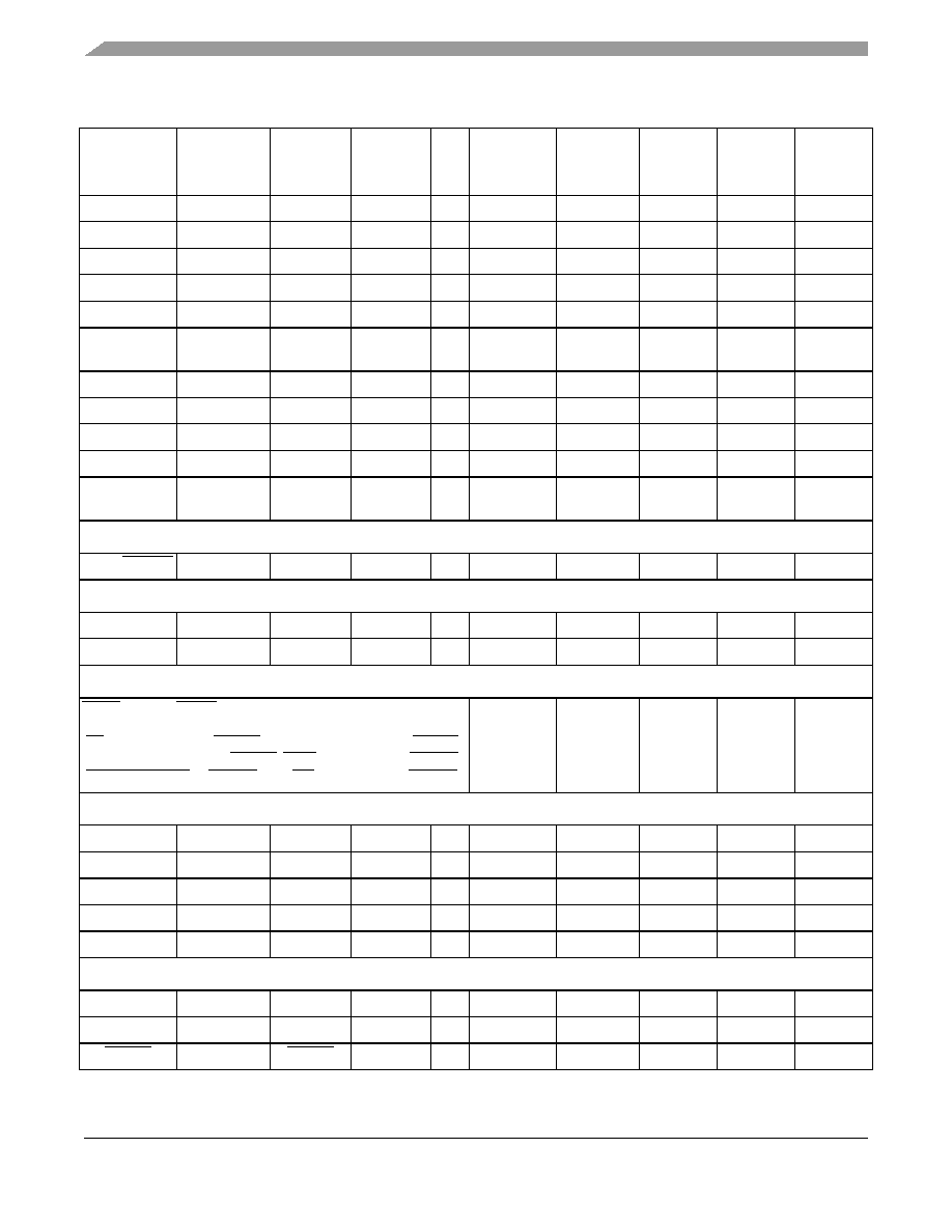
shows the behavior of SDRAM signals in synchronous mode.
Design Recommendations
MCF523x Integrated Microprocessor Hardware Specification, Rev. 1.3
Preliminary
Freescale Semiconductor
19
4.7.1.2
Address Multiplexing
Table 5
shows the generic address multiplexing scheme for SDRAM configurations. All possible address
connection configurations can be derived from this table.
Table 4. Synchronous DRAM Signal Connections
Signal
Description
SD_SRAS
Synchronous row address strobe. Indicates a valid SDRAM row address is present and can be
latched by the SDRAM. SD_SRAS should be connected to the corresponding SDRAM
SD_SRAS. Do not confuse SD_SRAS with the DRAM controller's SD_CS[1:0], which should not
be interfaced to the SDRAM SD_SRAS signals.
SD_SCAS
Synchronous column address strobe. Indicates a valid column address is present and can be
latched by the SDRAM. SD_SCAS should be connected to the corresponding signal labeled
SD_SCAS on the SDRAM.
DRAMW
DRAM read/write. Asserted for write operations and negated for read operations.
SD_CS[1:0]
Row address strobe. Select each memory block of SDRAMs connected to the MCF523x. One
SD_CS signal selects one SDRAM block and connects to the corresponding CS signals.
SD_CKE
Synchronous DRAM clock enable. Connected directly to the CKE (clock enable) signal of
SDRAMs. Enables and disables the clock internal to SDRAM. When CKE is low, memory can
enter a power-down mode where operations are suspended or they can enter self-refresh mode.
SD_CKE functionality is controlled by DCR[COC]. For designs using external multiplexing,
setting COC allows SD_CKE to provide command-bit functionality.
BS[3:0]
Column address strobe. For synchronous operation, BS[3:0] function as byte enables to the
SDRAMs. They connect to the DQM signals (or mask qualifiers) of the SDRAMs.
CLKOUT
Bus clock output. Connects to the CLK input of SDRAMs.
Table 5. Generic Address Multiplexing Scheme
Address Pin Row Address Column Address
Notes Related to Port Sizes
17
17
0
8-bit port only
16
16
1
8- and 16-bit ports only
15
15
2
14
14
3
13
13
4
12
12
5
11
11
6
10
10
7
9
9
8
17
17
16
32-bit port only
18
18
17
16-bit port only or 32-bit port with only 8
column address lines
19
19
18
16-bit port only when at least 9 column
address lines are used
20
20
19
MCF523x Integrated Microprocessor Hardware Specification, Rev. 1.3
Preliminary
Design Recommendations
Freescale Semiconductor
20
The following tables provide a more comprehensive, step-by-step way to determine the correct address
line connections for interfacing the MCF523x to SDRAM. To use the tables, find the one that corresponds
to the number of column address lines on the SDRAM and to the port size as seen by the MCF523x, which
is not necessarily the SDRAM port size. For example, if two 1M x 16-bit SDRAMs together form a
2M x 32-bit memory, the port size is 32 bits. Most SDRAMs likely have fewer address lines than are
shown in the tables, so follow only the connections shown until all SDRAM address lines are connected.
21
21
20
22
22
21
23
23
22
24
24
23
25
25
24
Table 6. MCF523x to SDRAM Interface (8-Bit Port, 9-Column Address Lines)
MCF523x
Pins
A17 A16 A15 A14 A13 A12 A11 A10 A9 A18 A19 A20 A21 A22 A23 A24 A25 A26 A27 A28 A29 A30 A31
Row
17
16
15
14
13
12
11
10
9
18
19
20
21
22
23
24
25
26
27
28
29
30
31
Column
0
1
2
3
4
5
6
7
8
SDRAM
Pins
A0 A1 A2 A3 A4 A5 A6 A7 A8 A9 A10 A11 A12 A13 A14 A15 A16 A17 A18 A19 A20 A21 A22
Table 7. MCF523x to SDRAM Interface (8-Bit Port,10-Column Address Lines)
MCF523x
Pins
A17 A16 A15 A14 A13 A12 A11 A10 A9 A19 A20 A21 A22 A23 A24 A25 A26 A27 A28 A29 A30 A31
Row
17
16
15
14
13
12
11
10
9
19
20
21
22
23
24
25
26
27
28
29
30
31
Column
0
1
2
3
4
5
6
7
8
18
SDRAM
Pins
A0
A1
A2
A3
A4
A5
A6
A7
A8
A9 A10 A11 A12 A13 A14 A15 A16 A17 A18 A19 A20 A21
Table 8. MCF523x to SDRAM Interface (8-Bit Port,11-Column Address Lines)
MCF523x
Pins
A17 A16 A15 A14 A13 A12 A11 A10 A9 A19 A21 A22 A23 A24 A25 A26 A27 A28 A29 A30 A31
Row
17
16
15
14
13
12
11
10
9
19
21
22
23
24
25
26
27
28
29
30
31
Column
0
1
2
3
4
5
6
7
8
18
20
SDRAM
Pins
A0
A1
A2
A3
A4
A5
A6
A7
A8
A9 A10 A11 A12 A13 A14 A15 A16 A17 A18 A19 A20
Table 5. Generic Address Multiplexing Scheme (continued)
Address Pin Row Address Column Address
Notes Related to Port Sizes
Design Recommendations
MCF523x Integrated Microprocessor Hardware Specification, Rev. 1.3
Preliminary
Freescale Semiconductor
21
Table 9. MCF523x to SDRAM Interface (8-Bit Port,12-Column Address Lines)
MCF523x
Pins
A17 A16 A15 A14 A13 A12 A11 A10 A9 A19 A21 A23 A24 A25 A26 A27 A28 A29 A30 A31
Row
17
16
15
14
13
12
11
10
9
19
21
23
24
25
26
27
28
29
30
31
Column
0
1
2
3
4
5
6
7
8
18
20
22
SDRAM
Pins
A0
A1
A2
A3
A4
A5
A6
A7
A8
A9 A10 A11 A12 A13 A14 A15 A16 A17 A18 A19
Table 10. MCF523x to SDRAM Interface (8-Bit Port,13-Column Address Lines)
MCF523x
Pins
A17 A16 A15 A14 A13 A12 A11 A10 A9 A19 A21 A23 A25 A26 A27 A28 A29 A30 A31
Row
17
16
15
14
13
12
11
10
9
19
21
23
25
26
27
28
29
30
31
Column
0
1
2
3
4
5
6
7
8
18
20
22
24
SDRAM
Pins
A0
A1
A2
A3
A4
A5
A6
A7
A8
A9 A10 A11 A12 A13 A14 A15 A16 A17 A18
Table 11. MCF523x to SDRAM Interface (16-Bit Port, 8-Column Address Lines)
MCF523x
Pins
A16 A15 A14 A13 A12 A11 A10 A9 A17 A18 A19 A20 A21 A22 A23 A24 A25 A26 A27 A28 A29 A30 A31
Row
16
15
14
13
12
11
10
9
17
18
19
20
21
22
23
24
25
26
27
28
29
30
31
Column
1
2
3
4
5
6
7
8
SDRAM
Pins
A0 A1 A2 A3 A4 A5 A6 A7 A8 A9 A10 A11 A12 A13 A14 A15 A16 A17 A18 A19 A20 A21 A22
Table 12. MCF523x to SDRAM Interface (16-Bit Port, 9-Column Address Lines)
MCF523x
Pins
A16 A15 A14 A13 A12 A11 A10 A9 A18 A19 A20 A21 A22 A23 A24 A25 A26 A27 A28 A29 A30 A31
Row
16
15
14
13
12
11
10
9
18
19
20
21
22
23
24
25
26
27
28
29
30
31
Column
1
2
3
4
5
6
7
8
17
SDRAM
Pins
A0
A1
A2
A3
A4
A5
A6
A7
A8
A9 A10 A11 A12 A13 A14 A15 A16 A17 A18 A19 A20 A21
Table 13. MCF523x to SDRAM Interface (16-Bit Port, 10-Column Address Lines)
MCF523x
Pins
A16 A15 A14 A13 A12 A11 A10 A9 A18 A20 A21 A22 A23 A24 A25 A26 A27 A28 A29 A30 A31
Row
16
15
14
13
12
11
10
9
18
20
21
22
23
24
25
26
27
28
29
30
31
Column
1
2
3
4
5
6
7
8
17
19
SDRAM
Pins
A0
A1
A2
A3
A4
A5
A6
A7
A8
A9 A10 A11 A12 A13 A14 A15 A16 A17 A18 A19 A20
MCF523x Integrated Microprocessor Hardware Specification, Rev. 1.3
Preliminary
Design Recommendations
Freescale Semiconductor
22
Table 14. MCF523x to SDRAM Interface (16-Bit Port, 11-Column Address Lines)
MCF523x
Pins
A16 A15 A14 A13 A12 A11 A10 A9 A18 A20 A22 A23 A24 A25 A26 A27 A28 A29 A30 A31
Row
16
15
14
13
12
11
10
9
18
20
22
23
24
25
26
27
28
29
30
31
Column
1
2
3
4
5
6
7
8
17
19
21
SDRAM
Pins
A0
A1
A2
A3
A4
A5
A6
A7
A8
A9 A10 A11 A12 A13 A14 A15 A16 A17 A18 A19
Table 15. MCF523x to SDRAM Interface (16-Bit Port, 12-Column Address Lines)
MCF523x
Pins
A16 A15 A14 A13 A12 A11 A10
A9
A18 A20 A22 A24 A25 A26 A27 A28 A29 A30 A31
Row
16
15
14
13
12
11
10
9
18
20
22
24
25
26
27
28
29
30
31
Column
1
2
3
4
5
6
7
8
17
19
21
23
SDRAM
Pins
A0
A1
A2
A3
A4
A5
A6
A7
A8
A9
A10 A11 A12 A13 A14 A15 A16 A17 A18
Table 16. MCF523x to SDRAM Interface (16-Bit Port, 13-Column-Address Lines)
MCF523x
Pins
A16 A15 A14 A13 A12 A11 A10
A9
A18 A20 A22 A24 A26 A27 A28 A29 A30 A31
Row
16
15
14
13
12
11
10
9
18
20
22
24
26
27
28
29
30
31
Column
1
2
3
4
5
6
7
8
17
19
21
23
25
SDRAM
Pins
A0
A1
A2
A3
A4
A5
A6
A7
A8
A9
A10 A11 A12 A13 A14 A15 A16 A17
Table 17. MCF523x to SDRAM Interface (32-Bit Port, 8-Column Address Lines)
MCF523x
Pins
A15 A14 A13 A12 A11 A10 A9 A17 A18 A19 A20 A21 A22 A23 A24 A25 A26 A27 A28 A29 A30 A31
Row
15
14
13
12
11
10
9
17
18
19
20
21
22
23
24
25
26
27
28
29
30
31
Column
2
3
4
5
6
7
8
16
SDRAM
Pins
A0
A1
A2
A3
A4
A5
A6
A7
A8
A9 A10 A11 A12 A13 A14 A15 A16 A17 A18 A19 A20 A21
Table 18. MCF523x to SDRAM Interface (32-Bit Port, 9-Column Address Lines)
MCF523x
Pins
A15 A14 A13 A12 A11 A10 A9 A17 A19 A20 A21 A22 A23 A24 A25 A26 A27 A28 A29 A30 A31
Row
15
14
13
12
11
10
9
17
19
20
21
22
23
24
25
26
27
28
29
30
31
Column
2
3
4
5
6
7
8
16
18
SDRAM
Pins
A0
A1
A2
A3
A4
A5
A6
A7
A8
A9 A10 A11 A12 A13 A14 A15 A16 A17 A18 A19 A20
Design Recommendations
MCF523x Integrated Microprocessor Hardware Specification, Rev. 1.3
Preliminary
Freescale Semiconductor
23
4.7.1.3
SDRAM Interfacing Example
The tables in the previous section can be used to configure the interface in the following example. To
interface one 2M
◊ 32-bit ◊ 4 bank SDRAM component (8 columns) to the MCF523x, the connections
would be as shown in
Table 22
.
4.7.2
Ethernet PHY Transceiver Connection
The FEC supports both an MII interface for 10/100 Mbps Ethernet and a seven-wire serial interface for 10
Mbps Ethernet. The interface mode is selected by R_CNTRL[MII_MODE]. In MII mode, the 802.3
standard defines and the FEC module supports 18 signals. These are shown in
Table 23
.
Table 19. MCF523x to SDRAM Interface (32-Bit Port, 10-Column Address Lines)
MCF523x
Pins
A15 A14 A13 A12 A11 A10 A9 A17 A19 A21 A22 A23 A24 A25 A26 A27 A28 A29 A30 A31
Row
15
14
13
12
11
10
9
17
19
21
22
23
24
25
26
27
28
29
30
31
Column
2
3
4
5
6
7
8
16
18
20
SDRAM
Pins
A0
A1
A2
A3
A4
A5
A6
A7
A8
A9 A10 A11 A12 A13 A14 A15 A16 A17 A18 A19
Table 20. MCF523x to SDRAM Interface (32-Bit Port, 11-Column Address Lines)
MCF523x
Pins
A15 A14 A13 A12 A11 A10
A9
A17 A19 A21 A23 A24 A25 A26 A27 A28 A29 A30 A31
Row
15
14
13
12
11
10
9
17
19
21
23
24
25
26
27
28
29
30
31
Column
2
3
4
5
6
7
8
16
18
20
22
SDRAM
Pins
A0
A1
A2
A3
A4
A5
A6
A7
A8
A9
A10 A11 A12 A13 A14 A15 A16 A17 A18
Table 21. MCF523x to SDRAM Interface (32-Bit Port, 12-Column Address Lines)
MCF523x
Pins
A15 A14 A13 A12 A11 A10
A9
A17 A19 A21 A23 A25 A26 A27 A28 A29 A30 A31
Row
15
14
13
12
11
10
9
17
19
21
23
25
26
27
28
29
30
31
Column
2
3
4
5
6
7
8
16
18
20
22
24
SDRAM
Pins
A0
A1
A2
A3
A4
A5
A6
A7
A8
A9
A10 A11 A12 A13 A14 A15 A16 A17
Table 22. SDRAM Hardware Connections
SDRAM
Pins
A0
A1
A2
A3
A4
A5
A6
A7
A8
A9
A10 = CMD
BA0
BA1
MCF523x
Pins
A15
A14
A13
A12
A11
A10
A9
A17
A18
A19
A20
A21
A22
MCF523x Integrated Microprocessor Hardware Specification, Rev. 1.3
Preliminary
Design Recommendations
Freescale Semiconductor
24
The serial mode interface operates in what is generally referred to as AMD mode. The MCF523x
configuration for seven-wire serial mode connections to the external transceiver are shown in
Table 24
.
Refer to the M523xEVB evaluation board user's manual for an example of how to connect an external
PHY. Schematics for this board are accessible at the MCF5235 site by navigating to:
http://www.freescale.com
.
Table 23. MII Mode
Signal Description
MCF523x Pin
Transmit clock
ETXCLK
Transmit enable
ETXEN
Transmit data
ETXD[3:0]
Transmit error
ETXER
Collision
ECOL
Carrier sense
ECRS
Receive clock
ERXCLK
Receive enable
ERXDV
Receive data
ERXD[3:0]
Receive error
ERXER
Management channel clock
EMDC
Management channel serial data
EMDIO
Table 24. Seven-Wire Mode Configuration
Signal Description
MCF523x Pin
Transmit clock
ETXCLK
Transmit enable
ETXEN
Transmit data
ETXD[0]
Collision
ECOL
Receive clock
ERXCLK
Receive enable
ERXDV
Receive data
ERXD[0]
Unused, configure as PB14
ERXER
Unused input, tie to ground
ECRS
Unused, configure as PB[13:11]
ERXD[3:1]
Unused output, ignore
ETXER
Unused, configure as PB[10:8]
ETXD[3:1]
Unused, configure as PB15
EMDC
Input after reset, connect to ground
EMDIO

Mechanicals/Pinouts and Part Numbers
MCF523x Integrated Microprocessor Hardware Specification, Rev. 1.3
Preliminary
Freescale Semiconductor
25
4.7.2.1
FlexCAN
The FlexCAN module interface to the CAN bus is composed of 2 pins: CANTX and CANRX, which are
the serial transmitted data and the serial received data. The use of an external CAN transceiver to interface
to the CAN bus is generally required. The transceiver is capable of driving the large current needed for the
CAN bus and has current protection, against a defective CAN bus or defective stations.
4.7.3
BDM
Use the BDM interface as shown in the M523xEVB evaluation board user's manual. The schematics for
this board are accessible at the MCF523x site by navigating from:
http://www.freescale.com
following the
32-bit Embedded Processors, 68K/ColdFire, MCF5xxx, MCF523x and M523xEVB links.
5
Mechanicals/Pinouts and Part Numbers
This section contains drawings showing the pinout and the packaging and mechanical characteristics of
the MCF523x devices. See
Table 2
for a list the signal names and pin locations for each device.
MCF523x Integrated Microprocessor Hardware Specification, Rev. 1.3
Preliminary
Mechanicals/Pinouts and Part Numbers
Freescale Semiconductor
26
5.1
Pinout--196 MAPBGA
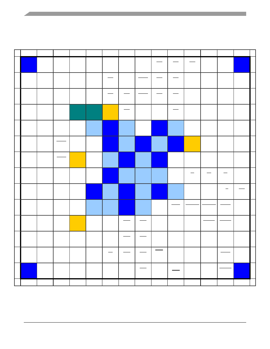
Figure 2
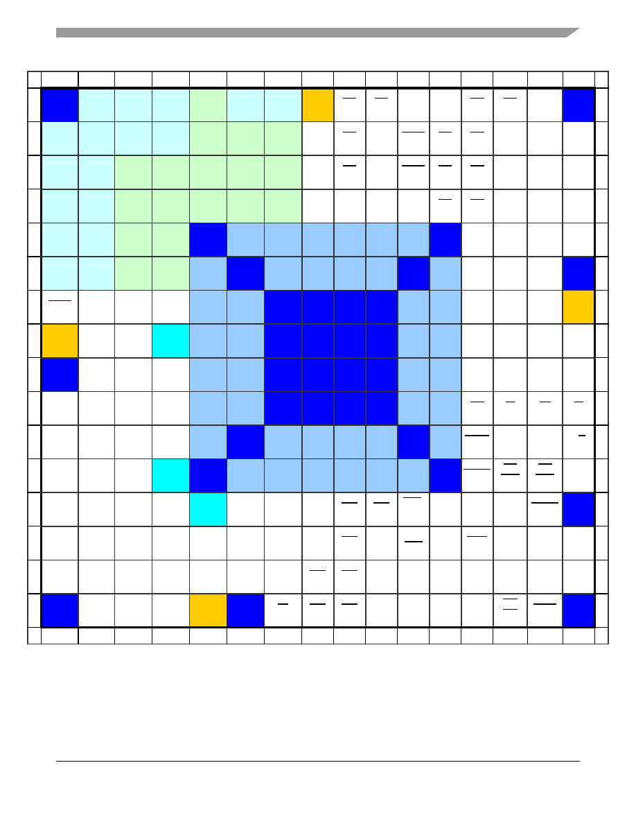
shows a pinout of the MCF5232CVMxxx package.
Figure 2. MCF5232CVMxxx Pinout (196 MAPBGA)
1
2
3
4
5
6
7
8
9
10
11
12
13
14
A
VSS
TPUCH6
TPUCH3
TPUCH2
QSPI_
DOUT
QSPI_CS0
U2RXD
U2TXD
CS3
CS6
CS4
A20
A17
VSS
A
B
TPUCH8
TPUCH7
TPUCH4
TPUCH0
QSPI_
DIN
BS3
QSPI_CS1
U1CTS
CS7
CS1
A23
A19
A16
A15
B
C
TPUCH10 TPUCH9
TPUCH5
TPUCH1 QSPI_CLK
BS2
BS0
U1RTS
CS2
CS5
A22
A18
A14
A13
C
D
TPUCH13 TPUCH12 TPUCH11
NC
NC
VDD
BS1
U1RXD/
CAN0RX
U1TXD/
CAN0TX
CS0
A21
A12
A11
A10
D
E
TPUCH14 TPUCH15 TCRCLK
DT0IN
OVDD
VSS
OVDD
SD_CKE
VSS
OVDD
A9
A8
A7
A6
E
F
U0TXD
U0RXD
U0CTS
DT0OUT
TEST
VSS
OVDD
VSS
OVDD
VSS
VDD
A5
A4
A3
F
G
D31
D30
U0RTS
VDD
CLKMOD1
OVDD
VSS
OVDD
VSS
LTPU
ODIS
A2
A1
A0
DT3OUT G
H
D29
D28
D27
D26
CLKMOD0
VSS
OVDD
OVDD
OVDD
UTPU
ODIS
TA
TIP
TS
DT3IN
H
J
D25
D24
D23
D22
VSS
OVDD
VSS
OVDD
VSS
OVDD
I2C_SCL
I2C_SDA
R/W
TEA
J
K
D21
D20
D19
D18
OVDD
OVDD
VSS
OVDD
JTAG_EN
RCON
SD_SRAS SD_SCAS
SD_WE
CLKOUT K
L
D17
D16
D10
VDD
D3
DT1IN
IRQ5
IRQ1
DT2OUT
PST0
DDATA0
SD_CS1
SD_CS0
VSSPLL
L
M
D15
D13
D9
D6
D2
DT1OUT
IRQ6
IRQ2
DT2IN
TDI/DSI
PST3
DDATA3
VDDPLL
EXTAL
M
N
D14
D12
D8
D5
D1
OE
IRQ7
IRQ3
TRST/
DSCLK
TDO/DSO
PST2
DDATA2
RESET
XTAL
N
P
VSS
D11
D7
D4
D0
TSIZ1
TSIZ0
IRQ4
TCLK/
PSTCLK
TMS/
BKPT
PST1
DDATA1
RSTOUT
VSS
P
1
2
3
4
5
6
7
8
9
10
11
12
13
14
Mechanicals/Pinouts and Part Numbers
MCF523x Integrated Microprocessor Hardware Specification, Rev. 1.3
Preliminary
Freescale Semiconductor
27
5.2
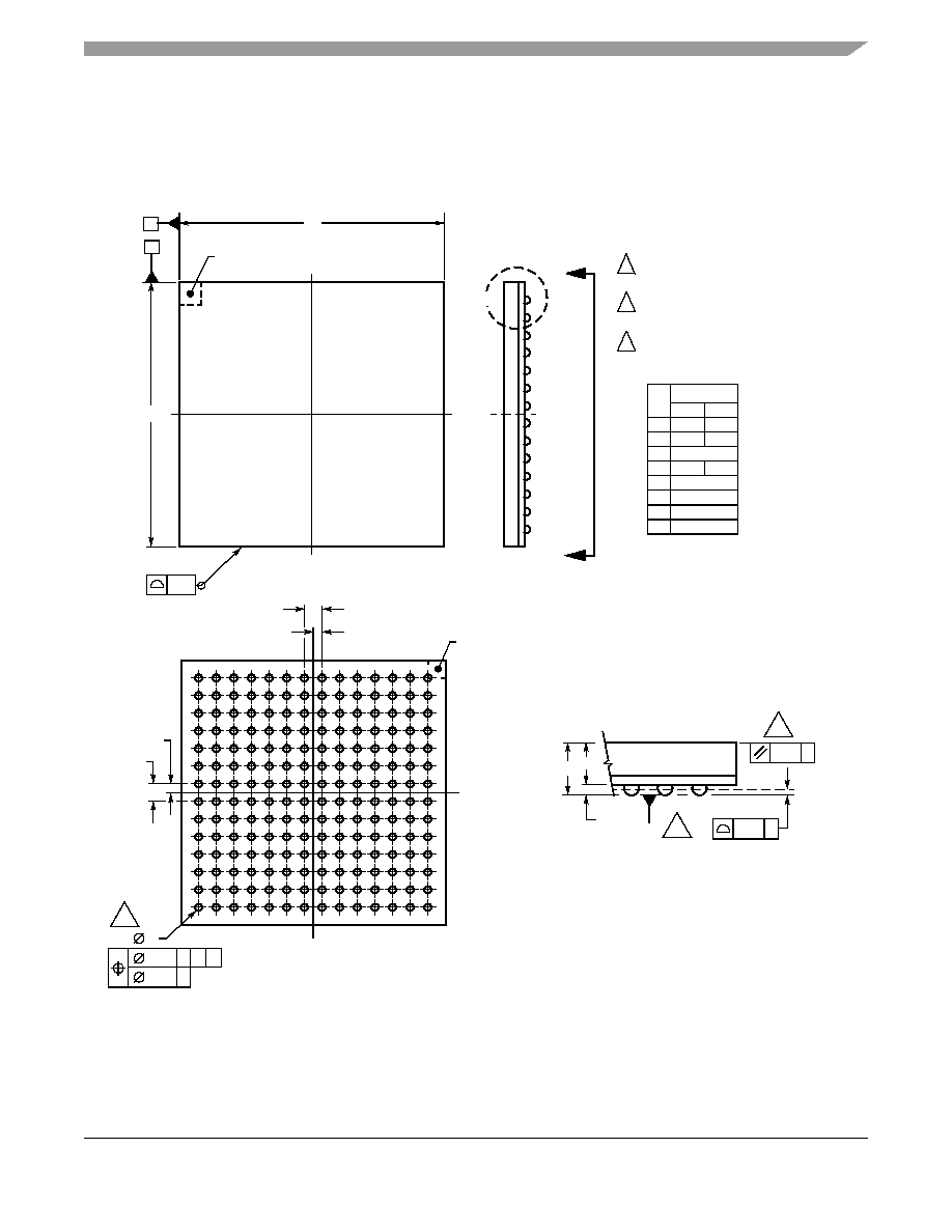
Package Dimensions--196 MAPBGA
Figure 3
shows MCF5232CVMxxx package dimensions.
Figure 3. 196 MAPBGA Package Dimensions (Case No. 1128A-01)
X
0.20
Laser mark for pin 1
identification in
this area
e
13X
D
E
M
S
A1
A2
A
0.15 Z
0.30 Z
Z
Rotated 90 Clockwise
Detail K
∞
5
View M-m
e
13X
S
M
X
0.30
Y
Z
0.10 Z
3
b
196X
Metalized mark for
pin 1 identification
in this area
14 13 12 11
5
4
3
2
B
C
D
E
F
G
H
J
K
L
4
NOTES:
1. Dimensions are in millimeters.
2. Interpret dimensions and tolerances
per ASME Y14.5M, 1994.
3. Dimension B is measured at the
maximum solder ball diameter,
parallel to datum plane Z.
4. Datum Z (seating plane) is defined
by the spherical crowns of the solder
balls.
5. Parallelism measurement shall
exclude any effect of mark on top
surface of package.
DIM
Min Max
Millimeters
A 1.32 1.75
A1 0.27 0.47
A2 1.18 REF
b 0.35 0.65
D 15.00 BSC
E 15.00 BSC
e
1.00 BSC
S
0.50 BSC
Y
K
M
N
P
A
1
6
10
9
MCF523x Integrated Microprocessor Hardware Specification, Rev. 1.3
Preliminary
Mechanicals/Pinouts and Part Numbers
Freescale Semiconductor
28
5.2.1
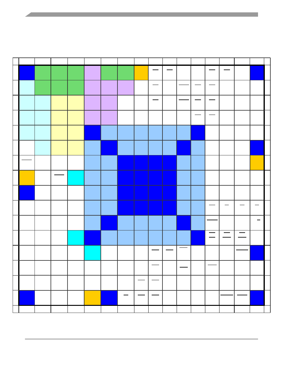
Pinout--256 MAPBGA
Figure 4
through
Figure 6
show pinouts of the MCF5233CVMxxx, MCF5234CVMxxx, and
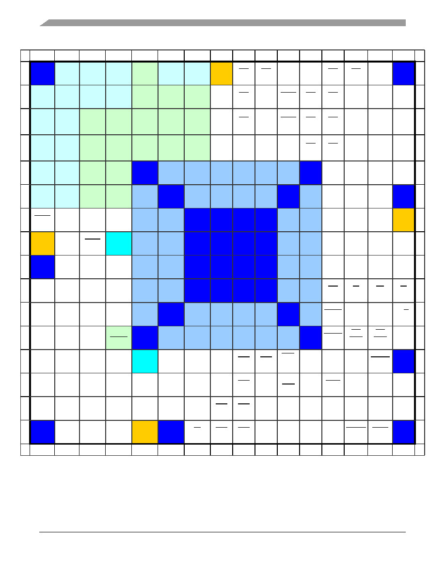
MCF5235CVMxxx packages.
Figure 4. MCF5233CVMxxx Pinout (256 MAPBGA)
1
2
3
4
5
6
7
8
9
10
11
12
13
14
15
16
A
VSS
TPUCH6
TPUCH4
TPUCH2 TPUCH17 TPUCH1
TPUCH0
VDD
BS1
BS0
U1RXD/
CAN0RX
U1TXD/
CAN0TX
CS6
CS4
A21
VSS
A
B
TPUCH8 TPUCH7
TPUCH5
TPUCH3 TPUCH18 TPUCH19 TPUCH16
QSPI_
CLK
BS2
QSPI_
CS1
U1RTS
CS3
CS1
A23
A20
A19
B
C
TPUCH10 TPUCH9 TPUCH25 TPUCH24 TPUCH22 TPUCH20
I2C_SDA/
U2RXD
QSPI_
DIN
BS3
SD_CKE U1CTS
CS7
CS5
A22
A18
A17
C
D
TPUCH12 TPUCH11 TPUCH27 TPUCH26 TPUCH23 TPUCH21
I2C_SCL/
U2TXD
QSPI_
DOUT
QSPI_
CS0
U2RXD/
CAN1RX
U2TXD/
CAN1TX
CS2
CS0
A14
A15
A16
D
E
TPUCH14 TPUCH13 TPUCH29 TPUCH28
VSS
OVDD
OVDD
OVDD
OVDD
OVDD
OVDD
VSS
A10
A11
A12
A13
E
F
TCRCLK TPUCH15 TPUCH31 TPUCH30
OVDD
VSS
OVDD
OVDD
OVDD
OVDD
VSS
OVDD
A7
A8
A9
VSS
F
G
U0CTS
U0RXD
DT0OUT
DT0IN
OVDD
OVDD
VSS
VSS
VSS
VSS
OVDD
OVDD
A4
A5
A6
VDD
G
H
VDD
U0TXD
U0RTS
NC
OVDD
OVDD
VSS
VSS
VSS
VSS
OVDD
OVDD
A0
A1
A2
A3
H
J
VSS
CLK
MOD0
CLK
MOD1
TEST
OVDD
OVDD
VSS
VSS
VSS
VSS
OVDD
OVDD
UTPU
ODIS
LTPU
ODIS
DT3IN
DT3OUT J
K
D28
D29
D30
D31
OVDD
OVDD
VSS
VSS
VSS
VSS
OVDD
OVDD
TEA
TA
TIP
TS
K
L
D24
D25
D26
D27
OVDD
VSS
OVDD
OVDD
OVDD
OVDD
VSS
OVDD
SD_WE
I2C_SCL/
CAN0TX
I2C_SDA/
CAN0RX
R/W
L
M
D21
D22
D23
NC
VSS
OVDD
OVDD
OVDD
OVDD
OVDD
OVDD
VSS
SD_
CS0
SD_
SRAS
SD_
SCAS
CLKOUT M
N
D19
D20
D13
D9
NC
D3
D0
TSIZ1
IRQ5
IRQ1
TRST/
DSCLK
PST0
JTAG_
EN
DDATA3 SD_CS1
VSS
N
P
D17
D18
D12
D8
D5
D2
DT1IN
TSIZ0
IRQ4
DT2IN
TMS/
BKPT
PST1
RCON
DDATA2 VDDPLL
EXTAL P
R
D16
D15
D11
D7
D4
D1
DT1OUT
IRQ7
IRQ3
DT2OUT
TDO/
DSO
PST2
DDATA0
PLL_
TEST
VSSPLL
XTAL
R
T
VSS
D14
D10
D6
VDD
VSS
OE
IRQ6
IRQ2
TCLK/
PSTCLK
TDI/DSI
PST3
DDATA1 RSTOUT RESET
VSS
T
1
2
3
4
5
6
7
8
9
10
11
12
13
14
15
16
Mechanicals/Pinouts and Part Numbers
MCF523x Integrated Microprocessor Hardware Specification, Rev. 1.3
Preliminary
Freescale Semiconductor
29
Figure 5. MCF5234CVMxxx Pinout (256 MAPBGA)
1
2
3
4
5
6
7
8
9
10
11
12
13
14
15
16
A
VSS
TPUCH6
TPUCH4
TPUCH2
ETXD1
TPUCH1
TPUCH0
VDD
BS1
BS0
U1RXD/
CAN0RX
U1TXD/
CAN0TX
CS6
CS4
A21
VSS
A
B
TPUCH8 TPUCH7
TPUCH5
TPUCH3
ETXD2
ETXD3
ETXD0
QSPI_
CLK
BS2
QSPI_
CS1
U1RTS
CS3
CS1
A23
A20
A19
B
C
TPUCH10 TPUCH9
ERXD1
ERXD0
ETXCLK
ETXER
EMDIO
QSPI_
DIN
BS3
SD_CKE U1CTS
CS7
CS5
A22
A18
A17
C
D
TPUCH12 TPUCH11
ERXD3
ERXD2
ERXER
ETXEN
EMDC
QSPI_
DOUT
QSPI_
CS0
U2RXD U2TXD
CS2
CS0
A14
A15
A16
D
E
TPUCH14 TPUCH13 ERXCLK
ERXDV
VSS
OVDD
OVDD
OVDD
OVDD
OVDD
OVDD
VSS
A10
A11
A12
A13
E
F
TCRCLK TPUCH15
ECOL
ECRS
OVDD
VSS
OVDD
OVDD
OVDD
OVDD
VSS
OVDD
A7
A8
A9
VSS
F
G
U0CTS
U0RXD
DT0OUT
DT0IN
OVDD
OVDD
VSS
VSS
VSS
VSS
OVDD
OVDD
A4
A5
A6
VDD
G
H
VDD
U0TXD
U0RTS
NC
OVDD
OVDD
VSS
VSS
VSS
VSS
OVDD
OVDD
A0
A1
A2
A3
H
J
VSS
CLK
MOD0
CLK
MOD1
TEST
OVDD
OVDD
VSS
VSS
VSS
VSS
OVDD
OVDD
UTPU
ODIS
LTPU
ODIS
DT3IN
DT3OUT J
K
D28
D29
D30
D31
OVDD
OVDD
VSS
VSS
VSS
VSS
OVDD
OVDD
TEA
TA
TIP
TS
K
L
D24
D25
D26
D27
OVDD
VSS
OVDD
OVDD
OVDD
OVDD
VSS
OVDD
SD_WE
I2C_SCL/
CAN0TX
I2C_SDA/
CAN0RX
R/W
L
M
D21
D22
D23
NC
VSS
OVDD
OVDD
OVDD
OVDD
OVDD
OVDD
VSS
SD_CS0
SD_
SRAS
SD_
SCAS
CLKOUT M
N
D19
D20
D13
D9
NC
D3
D0
TSIZ1
IRQ5
IRQ1
TRST/
DSCLK
PST0
JTAG_
EN
DDATA3 SD_CS1
VSS
N
P
D17
D18
D12
D8
D5
D2
DT1IN
TSIZ0
IRQ4
DT2IN
TMS/
BKPT
PST1
RCON
DDATA2 VDDPLL
EXTAL P
R
D16
D15
D11
D7
D4
D1
DT1OUT
IRQ7
IRQ3
DT2OUT
TDO/
DSO
PST2
DDATA0
PLL_
TEST
VSSPLL
XTAL
R
T
VSS
D14
D10
D6
VDD
VSS
OE
IRQ6
IRQ2
TCLK/
PSTCLK
TDI/DSI
PST3
DDATA1
RST
OUT
RESET
VSS
T
1
2
3
4
5
6
7
8
9
10
11
12
13
14
15
16
MCF523x Integrated Microprocessor Hardware Specification, Rev. 1.3
Preliminary
Mechanicals/Pinouts and Part Numbers
Freescale Semiconductor
30
Figure 6. MCF5235CVMxxx Pinout (256 MAPBGA)
1
2
3
4
5
6
7
8
9
10
11
12
13
14
15
16
A
VSS
TPUCH6 TPUCH4
TPUCH2
TPUCH17/
ETXD1
TPUCH1
TPUCH0
VDD
BS1
BS0
U1RXD/
CAN0RX
U1TXD/
CAN0TX
CS6
CS4
A21
VSS
A
B
TPUCH8 TPUCH7 TPUCH5
TPUCH3
TPUCH18/
ETXD2
TPUCH19/
ETXD3
TPUCH16/
ETXD0
QSPI_
CLK
BS2
QSPI_
CS1
U1RTS
CS3
CS1
A23
A20
A19
B
C
TPUCH10 TPUCH9
TPUCH25/
ERXD1
TPUCH24/
ERXD0
TPUCH22/
ETXCLK
TPUCH20/
ETXER
I2C_SDA/
U2RXD/
EMDIO
QSPI_
DIN
BS3
SD_CKE U1CTS
CS7
CS5
A22
A18
A17
C
D
TPUCH12 TPUCH11
TPUCH27/
ERXD3
TPUCH26/
ERXD2
TPUCH23/
ERXER
TPUCH21/
ETXEN
I2C_SCL/
U2TXD/
EMDC
QSPI_
DOUT
QSPI_
CS0
U2RXD/
CAN1RX
U2TXD/
CAN1TX
CS2
CS0
A14
A15
A16
D
E
TPUCH14 TPUCH13
TPUCH29/
ERXCLK
TPUCH2/
ERXDV
VSS
OVDD
OVDD
OVDD
OVDD
OVDD
OVDD
VSS
A10
A11
A12
A13
E
F
TCRCLK TPUCH15
TPUCH31/
ECOL
TPUCH30/
ECRS
OVDD
VSS
OVDD
OVDD
OVDD
OVDD
VSS
OVDD
A7
A8
A9
VSS
F
G
U0CTS
U0RXD
DT0OUT
DT0IN
OVDD
OVDD
VSS
VSS
VSS
VSS
OVDD
OVDD
A4
A5
A6
VDD
G
H
VDD
U0TXD
U0RTS
NC
OVDD
OVDD
VSS
VSS
VSS
VSS
OVDD
OVDD
A0
A1
A2
A3
H
J
VSS
CLK
MOD0
CLK
MOD1
TEST
OVDD
OVDD
VSS
VSS
VSS
VSS
OVDD
OVDD
UTPU
ODIS
LTPU
ODIS
DT3IN
DT3OUT J
K
D28
D29
D30
D31
OVDD
OVDD
VSS
VSS
VSS
VSS
OVDD
OVDD
TEA
TA
TIP
TS
K
L
D24
D25
D26
D27
OVDD
VSS
OVDD
OVDD
OVDD
OVDD
VSS
OVDD
SD_WE
I2C_SCL/
CAN0TX
I2C_SDA/
CAN0RX
R/W
L
M
D21
D22
D23
eTPU/
EthENB
VSS
OVDD
OVDD
OVDD
OVDD
OVDD
OVDD
VSS
SD_CS0
SD_
SRAS
SD_
SCAS
CLKOUT M
N
D19
D20
D13
D9
NC
D3
D0
TSIZ1
IRQ5
IRQ1
TRST/
DSCLK
PST0
JTAG_
EN
DDATA3 SD_CS1
VSS
N
P
D17
D18
D12
D8
D5
D2
DT1IN
TSIZ0
IRQ4
DT2IN
TMS/
BKPT
PST1
RCON
DDATA2 VDDPLL
EXTAL P
R
D16
D15
D11
D7
D4
D1
DT1OUT
IRQ7
IRQ3
DT2OUT
TDO/
DSO
PST2
DDATA0
PLL_
TEST
VSSPLL
XTAL
R
T
VSS
D14
D10
D6
VDD
VSS
OE
IRQ6
IRQ2
TCLK/
PSTCLK
TDI/DSI
PST3
DDATA1 RSTOUT RESET
VSS
T
1
2
3
4
5
6
7
8
9
10
11
12
13
14
15
16
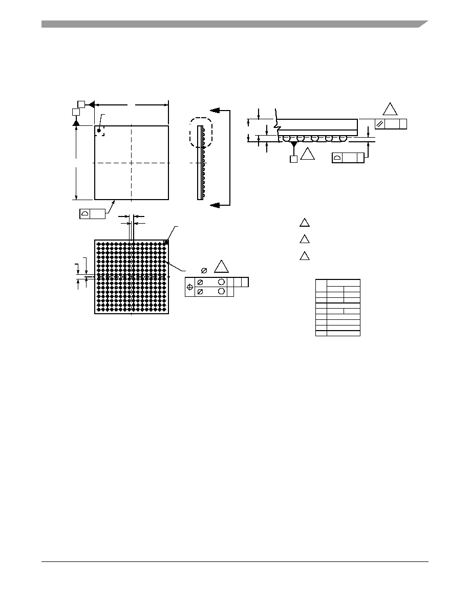
Mechanicals/Pinouts and Part Numbers
MCF523x Integrated Microprocessor Hardware Specification, Rev. 1.3
Preliminary
Freescale Semiconductor
31
5.2.2
Package Dimensions--256 MAPBGA
Figure 7
shows MCF5235CVMxxx, MCF5234CVMxxx, and MCF5233CVMxx package dimensions.
Figure 7. 256 MAPBGA Package Outline
X
Y
D
E
LASER MARK FOR PIN A1
IDENTIFICATION IN
THIS AREA
0.20
METALIZED MARK FOR
PIN A1 IDENTIFICATION
IN THIS AREA
M
M
3
A
B
C
D
E
F
G
H
J
K
L
M
N
P
R
T
1
2
3
4
5
6
7
10
11
12
13
14
15
16
e
15X
e
15X
b
256X
M
0.25
Y
Z
M
0.10
X
Z
S
DETAIL K
VIEW M-M
ROTATED 90 CLOCKWISE
∞
S
A
Z
Z
A2
A1
4
0.15
Z
0.30
256X
5
K
NOTES:
1.
DIMENSIONS ARE IN MILLIMETERS.
2.
INTERPRET DIMENSIONS AND
TOLERANCES PER ASME Y14.5M, 1994.
3.
DIMENSION b IS MEASURED AT THE
MAXIMUM SOLDER BALL DIAMETER,
PARALLEL TO DATUM PLANE Z.
4.
DATUM Z (SEATING PLANE) IS DEFINED BY
THE SPHERICAL CROWNS OF THE SOLDER
BALLS.
5.
PARALLELISM MEASUREMENT SHALL
EXCLUDE ANY EFFECT OF MARK ON TOP
SURFACE OF PACKAGE.
DIM
MIN
MAX
MILLIMETERS
A
1.25
1.60
A1
0.27
0.47
A2
1.16 REF
b
0.40
0.60
D
17.00 BSC
E
17.00 BSC
e
1.00 BSC
S
0.50 BSC
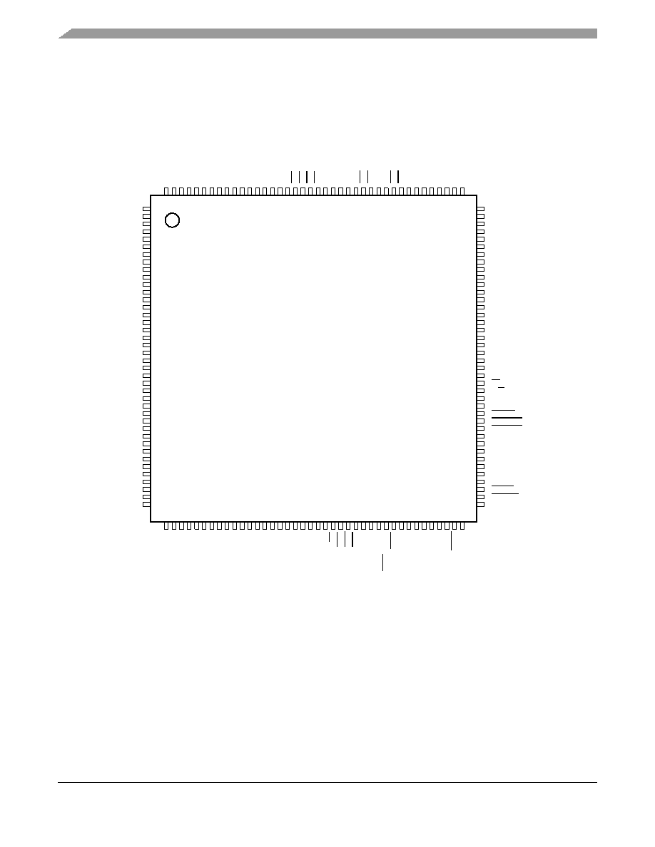
MCF523x Integrated Microprocessor Hardware Specification, Rev. 1.3
Preliminary
Mechanicals/Pinouts and Part Numbers
Freescale Semiconductor
32
5.3
Pinout--160 QFP
Figure 8
shows a pinout of the MCF5232CABxxx package.
Figure 8. MCF5232CABxxx Pinout (160 QFP)
16
0
15
9
15
8
15
7
15
6
15
5
15
4
15
3
15
2
15
1
15
0
14
9
14
8
14
7
14
6
14
5
14
4
14
3
14
2
14
1
14
0
13
9
13
8
13
7
13
6
13
5
13
4
13
3
13
2
13
1
13
0
12
9
12
8
12
7
12
6
12
5
12
4
12
3
12
2
12
1
120
119
118
117
116
115
114
113
112
111
110
109
108
107
106
105
104
103
102
101
100
99
98
97
96
95
94
93
92
91
90
89
88
87
86
85
84
83
82
81
41
42
43
44
45
46
47
48
49
50
51
52
53
54
55
56
57
58
59
60
61
62
63
64
65
66
67
68
69
70
71
72
73
74
75
76
77
78
79
80
1
2
3
4
5
6
7
8
9
10
11
12
13
14
15
16
17
18
19
20
21
22
23
24
25
26
27
28
29
30
31
32
33
34
35
36
37
38
39
40
VSS
TP
UCH
7
TP
UCH
6
TP
UCH
5
TP
UCH
4
TP
UCH
3
TP
UCH
2
VSS
TP
UCH
1
TP
UCH
0
QSP
I
_DOUT
QSP
I
_DIN
QSP
I
_C
LK
QSP
I
_CS0
OVDD
VSS
\OVS
S
VD
D
BS3
BS2
BS1
BS0
SD
_C
KE
\QS
PI_
C
S
1
OVDD
VSS
U1
RX
D\CA
N0R
X
U
1
T
X
D\
CA
N
0
T
X
CS
3
CS
2
OVDD
VSS
CS
1
CS
0
OVDD
VSS
A22
A21
A20
A19
A18
A17
A16
A15
A14
A13
A12
OVDD
VSS
A11
A10
A9
A8
A7
A6
A5
OVDD
VSS/OVSS
VDD
A4
A3
A2
A1
A0
TA
R/W
OVDD
VSS
SD_WE
SD_SCAS
SD_SRAS
OVDD
CLKOUT
VSS
VDDPLL
EXTAL
XTAL
VSSPLL
RESET
RSTOUT/PLL_TEST
OVDD
A23
OVDD
TPUCH8
TPUCH9
TPUCH10
TPUCH11
TPUCH12
TPUCH13
VSS
OVDD
TPUCH14
TPUCH15
TCRCLK
U0RXD
U0TXD
VDD
VSS
OVDD
TEST
CLKMOD1
CLKMOD0
D31
D30
D29
D28
VSS
D27
D26
D25
D24
D23
VSS
OVDD
D22
D21
D20
D19
D18
D17
D16
VSS
OVDD
D15
D14
D13
D12
D1
1
D10
D9
D8
D7
D6
D5
VD
D
VS
S\O
VSS
OVDD
D4
D3
D2
D1
D0
VS
S
OV
DD
OE
IRQ7
IRQ4
IRQ1
VS
S
TC
LK
\PSTC
L
K
OVDD
TRST
\DSCL
K
TM
S
\
BK
P
T
TDO/DSO
TD
I
/
DSI
PST0
PST1
PST2
PST3
JT
A
G
_E
N
RCON
VS
S
MCF5232
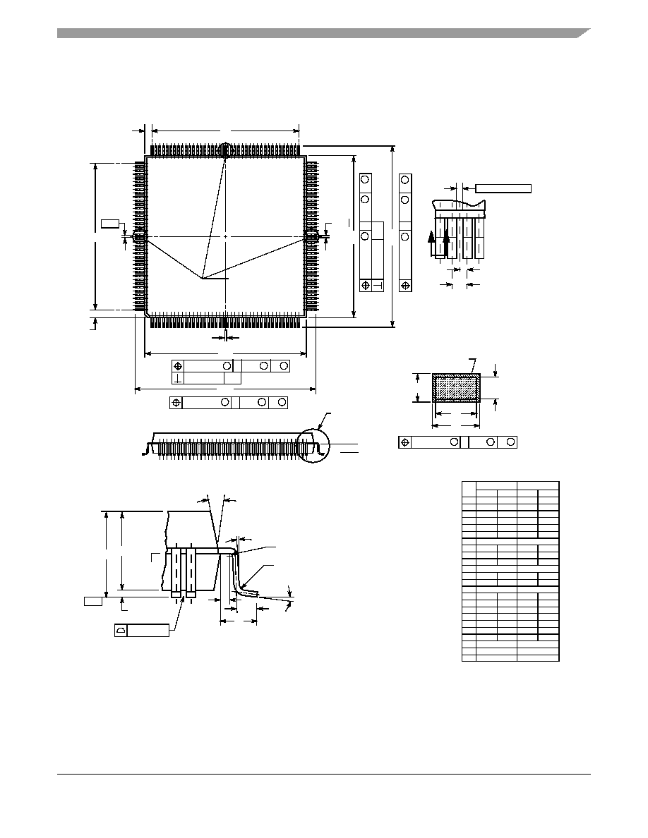
Mechanicals/Pinouts and Part Numbers
MCF523x Integrated Microprocessor Hardware Specification, Rev. 1.3
Preliminary
Freescale Semiconductor
33
5.4
Package Dimensions--160 QFP
Figure 9
shows MCF5232CAB80 package dimensions.
Figure 9. 160 QFP Package Dimensions
TOP &
BOTTOM
Case 864A-03
D
N
F
J
BASE
METAL
SECTION B≠B
DETAIL C
S
S
≠C≠
E
C
M
◊
U
◊
W
K
X
Q
◊
R
T
H
≠H≠
B
≠A≠, ≠B≠, ≠D≠
B
DETAIL A
G
P
S
S
S
S
S
S
A
S
L
Z
L
Y
DETAIL A
B
V
≠A≠
≠B≠
≠H≠
DETAIL C
MILLIMETERS
INCHES
DIM MIN
MAX
MIN
MAX
A
B
C
D
E
F
G
H
J
K
L
M
N
P
Q
R
T
U
V
W
X
Y
Z
27.90
28.10 1.098 1.106
27.90
28.10 1.098 1.106
3.35
3.85 0.132 1.106
3.35
3.85
0.009 0.015
0.22
0.38
0.009 0.013
0.22
0.33
0.126 0.138
3.20
3.50
0.65 BSC
0.026 REF
0.010 0.014
0.25
0.35
0.004 0.009
0.11
0.23
0.028 0.035
0.70
0.90
25.35 BSC
0.998 REF
5
∞
16
∞
5
∞
16
∞
0.004 0.007
0.11
0.19
0.325 BSC
0.013 REF
0
∞
7
∞
0
∞
7
∞
0.005 0.012
0.13
0.30
0.005
--
0.13
--
0
∞
--
0
∞
--
31.00
31.40 1.220 1.236
S
31.00
31.40 1.220 1.236
0.016
--
0.4
--
1.60 REF
0.063 REF
1.33 REF
0.052 REF
1.33 REF
0.052 REF
NOTES
1. DIMENSIONING AND TOLERINCING PER ANSI
Y14.5M, 1982.
2. CONTROLLING DIMENSION: MILLIMETER
3. DATUM PLAN -H- IS LOCATED AT BOTTOM OF
LEAD AND IS COINCIDENT WITH THE LEAD WHERE
THE LEAD EXITS THE PLASTIC BODY AT THE
BOTTOM OF THE PARTING LINE.
4. DATUMS -A-, -B-, AND -D- TO BE DETERMINED AT
DATUM PLANE -H-.
5. DIMENSIONS S AND V TO BE DETERMINED AT
SEATING PLANE -C-.
6. DIMENSIONS A AND B DO NOT INCLUDE MOLD
PROTRUSION. ALLOWABLE PROTRUSION IS 0.25
(0.010) PER SIDE. DIMENSIONS A AND B DO
INCLUDE MOLD MISMATCH AND ARE DETERMINED
AT DATUM PLANE -H-.
7. DIMENSION D DOES NOT INCLUDE DAMBAR
PROTRUSION. ALLOWABLE DAMBAR PROTRUSION
SHALL BE 0.08 (0.003) TOTAL IN EXCESS OF THE D
DIMENSION AT MAXIMUM MATERIAL CONDITION.
DAMBAR CANNOT BE LOCATED ON THE LOWER
RADIUS OR THE FOOT.
0.110 (0.004)
A-B
D
C
0.13 (0.005) M
0.20 (0.008)
A-B
D
C
M
M
0.20 (0.008)
A-B
0.20 (0.008)
A-B
D
C
S
S
M
M
H
A-B
D
H
A-
B
D
0
.
20 (0.008)
0.20 (
0
.008)
0.20 (0.0
08)
A-
B
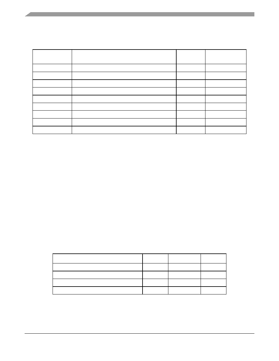
MCF523x Integrated Microprocessor Hardware Specification, Rev. 1.3
Preliminary
Preliminary Electrical Characteristics
Freescale Semiconductor
34
5.5
Ordering Information
6
Preliminary Electrical Characteristics
This chapter contains electrical specification tables and reference timing diagrams for the MCF5235
microcontroller unit. This section contains detailed information on power considerations, DC/AC
electrical characteristics, and AC timing specifications of MCF5235.
The electrical specifications are preliminary and are from previous designs or design simulations. These
specifications may not be fully tested or guaranteed at this early stage of the product life cycle, however
for production silicon these specifications will be met. Finalized specifications will be published after
complete characterization and device qualifications have been completed.
NOTE
The parameters specified in this processor document supersede any values
found in the module specifications.
6.1
Maximum Ratings
Table 25. Orderable Part Numbers
Freescale Part
Number
Description
Speed
Temperature
MCF5232CAB80
MCF5232 RISC Microprocessor, 160 QFP
80MHz
≠40
∞
to +85
∞
C
MCF5232CVM100
MCF5232 RISC Microprocessor, 196 MAPBGA
100MHz
≠40
∞
to +85
∞
C
MCF5232CVM150
MCF5232 RISC Microprocessor, 196 MAPBGA
150MHz
≠40
∞
to +85
∞
C
MCF5233CVM100
MCF5233 RISC Microprocessor, 256 MAPBGA
100MHz
≠40
∞
to +85
∞
C
MCF5233CVM150
MCF5233 RISC Microprocessor, 256 MAPBGA
150MHz
≠40
∞
to +85
∞
C
MCF5234CVM100
MCF5234 RISC Microprocessor, 256 MAPBGA
100MHz
≠40
∞
to +85
∞
C
MCF5234CVM150
MCF5234 RISC Microprocessor, 256 MAPBGA
150MHz
≠40
∞
to +85
∞
C
MCF5235CVM100
MCF5235 RISC Microprocessor, 256 MAPBGA
100MHz
≠40
∞
to +85
∞
C
MCF5235CVM150
MCF5235 RISC Microprocessor, 256 MAPBGA
150MHz
≠40
∞
to +85
∞
C
Table 26. Absolute Maximum Ratings
1,
2
Rating
Symbol
Value
Unit
Core Supply Voltage
V
DD
≠ 0.5 to +2.0
V
Pad Supply Voltage
OV
DD
≠ 0.3 to +4.0
V
Clock Synthesizer Supply Voltage
V
DDPLL
≠ 0.3 to +4.0
V
Digital Input Voltage
3
V
IN
≠ 0.3 to + 4.0
V
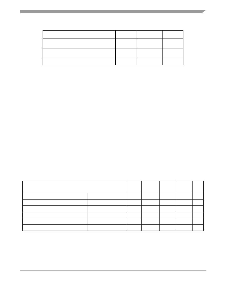
Preliminary Electrical Characteristics
MCF523x Integrated Microprocessor Hardware Specification, Rev. 1.3
Preliminary
Freescale Semiconductor
35
6.2
Thermal Characteristics
Table 27
lists thermal resistance values
Instantaneous Maximum Current
Single pin limit (applies to all pins)
3,4,5
I
D
25
mA
Operating Temperature Range (Packaged)
T
A
(T
L
- T
H
)
≠ 40 to 85
∞C
Storage Temperature Range
T
stg
≠ 65 to 150
∞C
NOTES:
1
Functional operating conditions are given in DC Electrical Specifications. Absolute Maximum
Ratings are stress ratings only, and functional operation at the maxima is not guaranteed.
Continued operation at these levels may affect device reliability or cause permanent damage
to the device.
2
This device contains circuitry protecting against damage due to high static voltage or
electrical fields; however, it is advised that normal precautions be taken to avoid application of
any voltages higher than maximum-rated voltages to this high-impedance circuit. Reliability of
operation is enhanced if unused inputs are tied to an appropriate logic voltage level (e.g.,
either V
SS
or OV
DD
).
3
Input must be current limited to the value specified. To determine the value of the required
current-limiting resistor, calculate resistance values for positive and negative clamp voltages,
then use the larger of the two values.
4
All functional non-supply pins are internally clamped to V
SS
and OV
DD
.
5
Power supply must maintain regulation within operating OV
DD
range during instantaneous
and operating maximum current conditions. If positive injection current (V
in
> OV
DD
) is greater
than I
DD
, the injection current may flow out of OV
DD
and could result in external power supply
going out of regulation. Insure external OV
DD
load will shunt current greater than maximum
injection current. This will be the greatest risk when the processor is not consuming power
(ex; no clock).Power supply must maintain regulation within operating OV
DD
range during
instantaneous and operating maximum current conditions.
Table 27. Thermal Characteristics
Characteristic
Symbol
256
MAPBGA
196
MAPBGA
160QFP
Unit
Junction to ambient, natural convection
Four layer board (2s2p)
JMA
26
1,2
32
3,4
40
5,6
∞C / W
Junction to ambient (@200 ft/min)
Four layer board (2s2p)
JMA
23
5
,
6
29
5
,
6
36
5
,
6
∞C / W
Junction to board
JB
15
7
20
8
25
9
∞C / W
Junction to case
JC
10
10
10
11
10
12
∞C / W
Junction to top of package
jt
2
5
,13
2
5
,14
2
5
,15
∞C / W
Maximum operating junction temperature
T
j
TBD
TBD
TBD
o
C
Table 26. Absolute Maximum Ratings
1,
2
Rating
Symbol
Value
Unit

MCF523x Integrated Microprocessor Hardware Specification, Rev. 1.3
Preliminary
Preliminary Electrical Characteristics
Freescale Semiconductor
36
NOTES:
1
JMA
and
jt
parameters are simulated in conformance with EIA/JESD Standard 51-2 for natural convection. Freescale
recommends the use of
JmA
and power dissipation specifications in the system design to prevent device junction
temperatures from exceeding the rated specification. System designers should be aware that device junction
temperatures can be significantly influenced by board layout and surrounding devices. Conformance to the device
junction temperature specification can be verified by physical measurement in the customer's system using the
jt
parameter, the device power dissipation, and the method described in EIA/JESD Standard 51-2.
2
Per JEDEC JESD51-6 with the board horizontal.
3
JMA
and
jt
parameters are simulated in conformance with EIA/JESD Standard 51-2 for natural convection. Freescale
recommends the use of
JmA
and power dissipation specifications in the system design to prevent device junction
temperatures from exceeding the rated specification. System designers should be aware that device junction
temperatures can be significantly influenced by board layout and surrounding devices. Conformance to the device
junction temperature specification can be verified by physical measurement in the customer's system using the
jt
parameter, the device power dissipation, and the method described in EIA/JESD Standard 51-2.
4
Per JEDEC JESD51-6 with the board horizontal.
5
JMA
and
jt
parameters are simulated in conformance with EIA/JESD Standard 51-2 for natural convection. Freescale
recommends the use of
JmA
and power dissipation specifications in the system design to prevent device junction
temperatures from exceeding the rated specification. System designers should be aware that device junction
temperatures can be significantly influenced by board layout and surrounding devices. Conformance to the device
junction temperature specification can be verified by physical measurement in the customer's system using the
jt
parameter, the device power dissipation, and the method described in EIA/JESD Standard 51-2.
6
Per JEDEC JESD51-6 with the board horizontal.
7
Thermal resistance between the die and the printed circuit board in conformance with JEDEC JESD51-8. Board
temperature is measured on the top surface of the board near the package.
8
Thermal resistance between the die and the printed circuit board in conformance with JEDEC JESD51-8. Board
temperature is measured on the top surface of the board near the package.
9
Thermal resistance between the die and the printed circuit board in conformance with JEDEC JESD51-8. Board
temperature is measured on the top surface of the board near the package.
10
Thermal resistance between the die and the case top surface as measured by the cold plate method (MIL SPEC-883
Method 1012.1).
11
Thermal resistance between the die and the case top surface as measured by the cold plate method (MIL SPEC-883
Method 1012.1).
12
Thermal resistance between the die and the case top surface as measured by the cold plate method (MIL SPEC-883
Method 1012.1).
13
Thermal characterization parameter indicating the temperature difference between package top and the junction
temperature per JEDEC JESD51-2. When Greek letters are not available, the thermal characterization parameter is
written in conformance with Psi-JT.
14
Thermal characterization parameter indicating the temperature difference between package top and the junction
temperature per JEDEC JESD51-2. When Greek letters are not available, the thermal characterization parameter is
written in conformance with Psi-JT.
15
Thermal characterization parameter indicating the temperature difference between package top and the junction
temperature per JEDEC JESD51-2. When Greek letters are not available, the thermal characterization parameter is
written in conformance with Psi-JT.
The average chip-junction temperature (T
J
) in
∞C can be obtained from:
(1)
Where:
T
A
= Ambient Temperature,
∞C
JMA
= Package Thermal Resistance, Junction-to-Ambient,
∞C/W
P
D
= P
INT
+ P
I/O
P
INT
= I
DD
◊ V
DD
, Watts - Chip Internal Power
T
J
T
A
P
D
JMA
◊
(
)
+
=
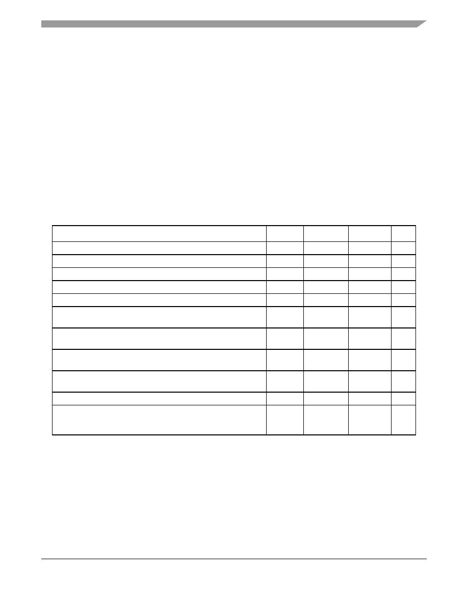
Preliminary Electrical Characteristics
MCF523x Integrated Microprocessor Hardware Specification, Rev. 1.3
Preliminary
Freescale Semiconductor
37
6.3
DC Electrical Specifications
P
I/O
= Power Dissipation on Input and Output Pins -- User Determined
For most applications P
I/O
< P
INT
and can be ignored. An approximate relationship between P
D
and T
J
(if P
I/O
is neglected) is:
(2)
Solving equations 1 and 2 for K gives:
K = P
D
◊ (T
A
+ 273
∞C) +
JMA
◊ P
D
2
(3)
where K is a constant pertaining to the particular part. K can be determined from equation (3)
by measuring P
D
(at equilibrium) for a known T
A
. Using this value of K, the values of P
D
and
T
J
can be obtained by solving equations (1) and (2) iteratively for any value of T
A
.
Table 28. DC Electrical Specifications
1
Characteristic
Symbol
Min
Max
Unit
Core Supply Voltage
V
DD
1.35
1.65
V
Pad Supply Voltage
OV
DD
3
3.6
V
Input High Voltage
V
IH
0.7
◊
OV
DD
3.65
V
Input Low Voltage
V
IL
V
SS
≠ 0.3
0.35
◊
OV
DD
V
Input Hysteresis
V
HYS
0.06
◊
OV
DD
--
mV
Input Leakage Current
V
in
= V
DD
or V
SS
, Input-only pins
I
in
≠1.0
1.0
µA
High Impedance (Off-State) Leakage Current
V
in
= V
DD
or V
SS
, All input/output and output pins
I
OZ
≠1.0
1.0
µA
Output High Voltage (All input/output and all output pins)
I
OH
= ≠5.0 mA
V
OH
OV
DD
- 0.5
__
V
Output Low Voltage (All input/output and all output pins)
I
OL
= 5.0mA
V
OL
__
0.5
V
Weak Internal Pull Up Device Current, tested at V
IL
Max.
2
I
APU
≠10
≠ 130
µA
Input Capacitance
3
All input-only pins
All input/output (three-state) pins
C
in
--
--
7
7
pF
P
D
K
T
J
273
∞C
+
(
)
˜
=
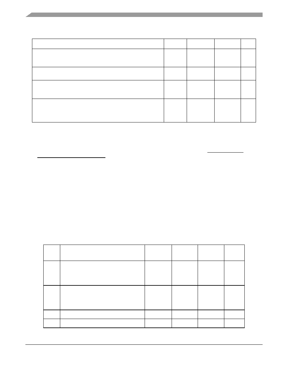
MCF523x Integrated Microprocessor Hardware Specification, Rev. 1.3
Preliminary
Preliminary Electrical Characteristics
Freescale Semiconductor
38
6.4
Oscillator and PLLMRFM Electrical Characteristics
Load Capacitance
4
Low drive strength
High drive strength
C
L
25
50
pF
Core Operating Supply Current
5
Master Mode
I
DD
--
TBD
mA
Pad Operating Supply Current
Master Mode
Low Power Modes
OI
DD
--
--
TBD
TBD
mA
µA
DC Injection Current
3,
6, 7, 8
V
NEGCLAMP
=V
SS
≠ 0.3 V, V
POSCLAMP
= V
DD
+ 0.3
Single Pin Limit
Total processor Limit, Includes sum of all stressed pins
I
IC
≠1.0
≠10
1.0
10
mA
NOTES:
1
Refer to Table 29 for additional PLL specifications.
2
Refer to the MCF5235 signals section for pins having weak internal pull-up devices.
3
This parameter is characterized before qualification rather than 100% tested.
4
pF load ratings are based on DC loading and are provided as an indication of driver strength. High speed interfaces
require transmission line analysis to determine proper drive strength and termination. See High Speed Signal
Propagation: Advanced Black Magic by Howard W. Johnson for design guidelines.
5
Current measured at maximum system clock frequency, all modules active, and default drive strength with matching
load.
6
All functional non-supply pins are internally clamped to V
SS
and their respective V
DD
.
7
Input must be current limited to the value specified. To determine the value of the required current-limiting resistor,
calculate resistance values for positive and negative clamp voltages, then use the larger of the two values.
8
Power supply must maintain regulation within operating V
DD
range during instantaneous and operating maximum
current conditions. If positive injection current (V
in
> V
DD
) is greater than I
DD
, the injection current may flow out of V
DD
and could result in external power supply going out of regulation. Insure external V
DD
load will shunt current greater
than maximum injection current. This will be the greatest risk when the processor is not consuming power. Examples
are: if no system clock is present, or if clock rate is very low which would reduce overall power consumption. Also, at
power-up, system clock is not present during the power-up sequence until the PLL has attained lock.
Table 29. HiP7 PLLMRFM Electrical Specifications
1
Num
Characteristic
Symbol
Min.
Value
Max.
Value
Unit
1
PLL Reference Frequency Range
Crystal reference
External reference
1:1 mode (NOTE: f
sys/2
= 2
◊ f
ref_1:1
)
f
ref_crystal
f
ref_ext
f
ref_1:1
8
8
24
25
25
75
MHz
2
Core frequency
CLKOUT Frequency
2
External reference
On-Chip PLL Frequency
f
sys
f
sys/2
0
f
ref
˜ 32
150
75
75
MHz
MHz
MHz
3
Loss of Reference Frequency
3, 5
f
LOR
100
1000
kHz
4
Self Clocked Mode Frequency
4, 5
f
SCM
TBD
TBD
MHz
Table 28. DC Electrical Specifications
1
Characteristic
Symbol
Min
Max
Unit
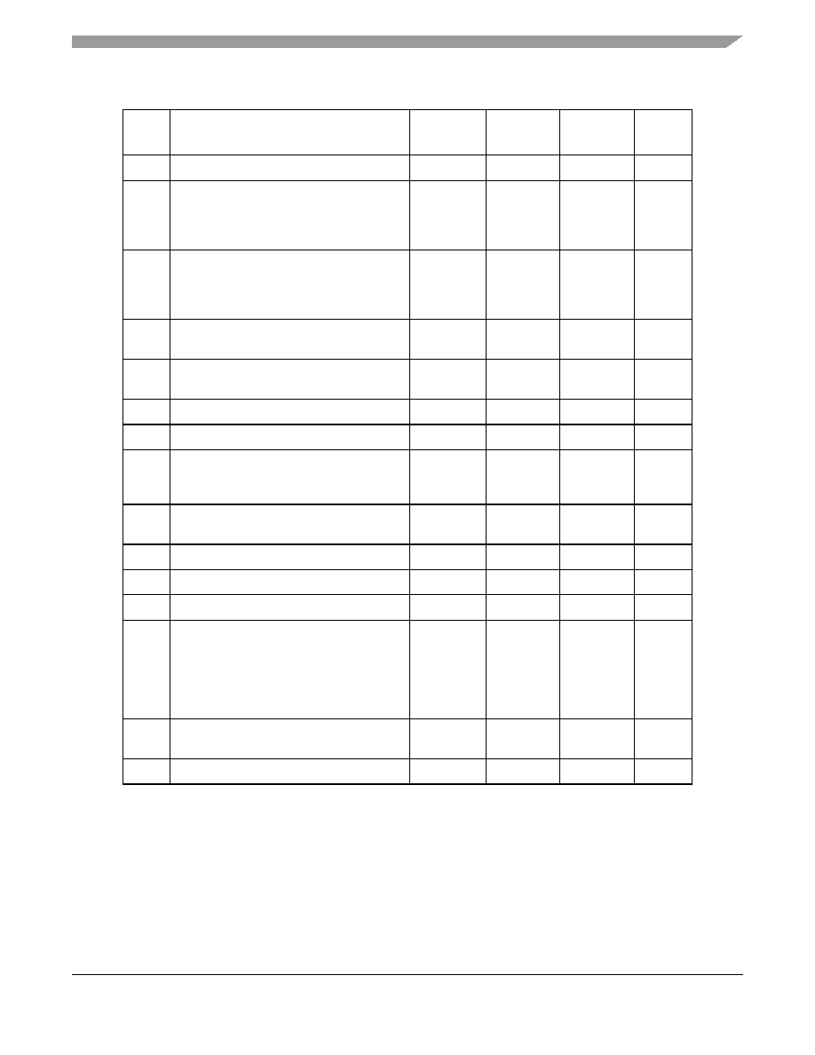
Preliminary Electrical Characteristics
MCF523x Integrated Microprocessor Hardware Specification, Rev. 1.3
Preliminary
Freescale Semiconductor
39
5
Crystal Start-up Time
5, 6
t
cst
--
10
ms
6
EXTAL Input High Voltage
Crystal Mode
7
All other modes (Dual Controller (1:1),
Bypass, External)
V
IHEXT
V
IHEXT
TBD
TBD
TBD
TBD
V
V
7
EXTAL Input Low Voltage
Crystal Mode
7
All other modes (Dual Controller (1:1),
Bypass, External)
V
ILEXT
V
ILEXT
TBD
TBD
TBD
TBD
V
V
8
XTAL Output High Voltage
I
OH
= 1.0 mA
V
OH
TBD
--
V
9
XTAL Output Low Voltage
I
OL
= 1.0 mA
V
OL
--
TBD
V
10
XTAL Load Capacitance
5
5
30
pF
11
PLL Lock Time
5, 8,14
t
lpll
--
750
µs
12
Power-up To Lock Time
5, 6,9
With Crystal Reference (includes 5 time)
Without Crystal Reference
10
t
lplk
--
--
11
750
ms
µs
13
1:1 Mode Clock Skew (between CLKOUT
and EXTAL)
11
t
skew
≠1
1
ns
14
Duty Cycle of reference
5
t
dc
40
60
%
15
Frequency un-LOCK Range
f
UL
≠3.8
4.1
% f
sys/2
16
Frequency LOCK Range
f
LCK
≠1.7
2.0
%
f
sys/2
17
CLKOUT Period Jitter,
5, 6, 9,12, 13
Measured at f
sys/2
Max
Peak-to-peak Jitter (Clock edge to clock
edge)
Long Term Jitter (Averaged over 2 ms
interval)
C
jitter
--
--
5.0
.01
% f
sys/2
18
Frequency Modulation Range Limit
14
,
15
(f
sys/2
Max must not be exceeded)
C
mod
0.8
2.2
%f
sys/2
19
ICO Frequency. f
ico
= f
ref
*
2
*
(MFD+2)
16
f
ico
48
75
MHz
NOTES:
1
All values given are initial design targets and subject to change.
2
All internal registers retain data at 0 Hz.
3
"Loss of Reference Frequency" is the reference frequency detected internally, which transitions the PLL
into self clocked mode.
4
Self clocked mode frequency is the frequency that the PLL operates at when the reference frequency falls
below f
LOR
with default MFD/RFD settings.
5
This parameter is guaranteed by characterization before qualification rather than 100% tested.
6
Proper PC board layout procedures must be followed to achieve specifications.
7
This parameter is guaranteed by design rather than 100% tested.
Table 29. HiP7 PLLMRFM Electrical Specifications
1
Num
Characteristic
Symbol
Min.
Value
Max.
Value
Unit
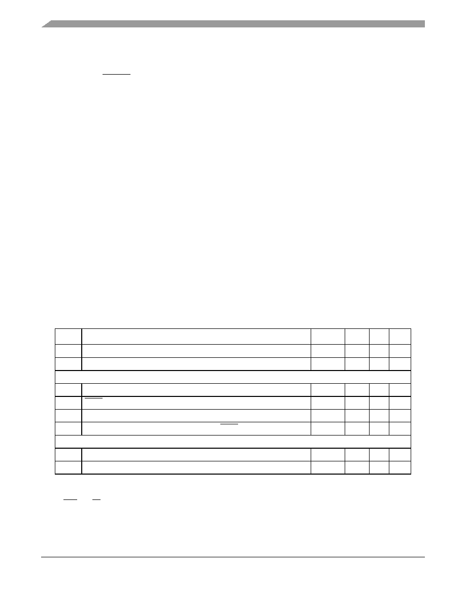
MCF523x Integrated Microprocessor Hardware Specification, Rev. 1.3
Preliminary
Preliminary Electrical Characteristics
Freescale Semiconductor
40
6.5
External Interface Timing Characteristics
Table 30
lists processor bus input timings.
NOTE
All processor bus timings are synchronous; that is, input setup/hold and
output delay with respect to the rising edge of a reference clock. The
reference clock is the CLKOUT output.
All other timing relationships can be derived from these values.
8
This specification applies to the period required for the PLL to relock after changing the MFD frequency
control bits in the synthesizer control register (SYNCR).
9
Assuming a reference is available at power up, lock time is measured from the time V
DD
and V
DDSYN
are
valid to RSTOUT negating. If the crystal oscillator is being used as the reference for the PLL, then the
crystal start up time must be added to the PLL lock time to determine the total start-up time.
10
t
lpll
= (64
*
4
*
5 + 5
◊
)
◊
T
ref
, where T
ref
= 1/F
ref_crystal
= 1/F
ref_ext
= 1/F
ref_1:1
, and
= 1.57x10
-6
◊
2(MFD + 2).
11
PLL is operating in 1:1 PLL mode.
12
Jitter is the average deviation from the programmed frequency measured over the specified interval at
maximum f
sys/2
. Measurements are made with the device powered by filtered supplies and clocked by a
stable external clock signal. Noise injected into the PLL circuitry via V
DDSYN
and V
SSSYN
and variation in
crystal oscillator frequency increase the Cjitter percentage for a given interval.
13
Values are with frequency modulation disabled. If frequency modulation is enabled, jitter is the sum of
Cjitter+Cmod.
14
Modulation percentage applies over an interval of 10
µs, or equivalently the modulation rate is 100KHz.
15
Modulation rate selected must not result in f
sys/2
value greater than the f
sys/2
maximum specified value.
Modulation range determined by hardware design.
16
f
sys/2
= f
ico
/ (2
*
2
RFD
)
Table 30. Processor Bus Input Timing Specifications
Name
Characteristic
1
NOTES:
1
Timing specifications are tested using full drive strength pad configurations in a 50ohm transmission line
environment..
Symbol
Min
Max
Unit
freq
System bus frequency
f
sys/2
50
50
MHz
B0
CLKOUT period
t
cyc
1/50
ns
Control Inputs
B1a
Control input valid to CLKOUT high
2
2
TEA and TA pins are being referred to as control inputs.
t
CVCH
9
--
ns
B1b BKPT valid to CLKOUT high
3
3
Refer to figure A-19.
t
BKVCH
9
--
ns
B2a
CLKOUT high to control inputs invalid
2
t
CHCII
0
--
ns
B2b
CLKOUT high to asynchronous control input BKPT invalid
3
t
BKNCH
0
--
ns
Data Inputs
B4
Data input (D[31:0]) valid to CLKOUT high
t
DIVCH
4
--
ns
B5
CLKOUT high to data input (D[31:0]) invalid
t
CHDII
0
--
ns
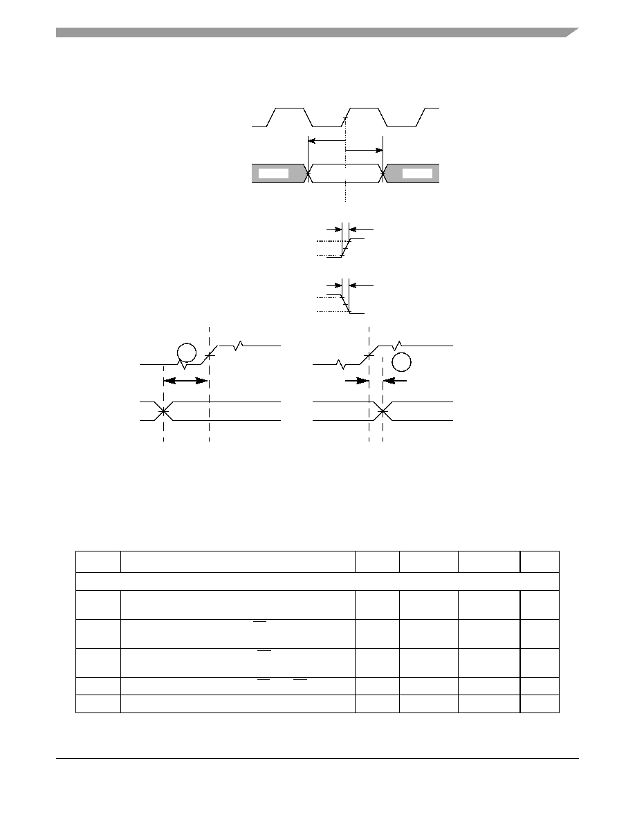
Preliminary Electrical Characteristics
MCF523x Integrated Microprocessor Hardware Specification, Rev. 1.3
Preliminary
Freescale Semiconductor
41
Timings listed in
Table 30
are shown in
Figure 10
& Figure A-3.
Figure 10. General Input Timing Requirements
6.6
Processor Bus Output Timing Specifications
Table 31
lists processor bus output timings.
Table 31. External Bus Output Timing Specifications
Name
Characteristic
Symbol
Min
Max
Unit
Control Outputs
B6a
CLKOUT high to chip selects valid
1
t
CHCV
--
0.5t
CYC
+5
ns
B6b
CLKOUT high to byte enables (BS[3:0]) valid
2
t
CHBV
--
0.5t
CYC
+5
ns
B6c
CLKOUT high to output enable (OE) valid
3
t
CHOV
--
0.5t
CYC
+5
ns
B7
CLKOUT high to control output (BS[3:0], OE) invalid
t
CHCOI
0.5t
CYC
+1.5
--
ns
B7a
CLKOUT high to chip selects invalid
t
CHCI
0.5t
CYC
+1.5
--
ns
Invalid
Invalid
CLKOUT(75MHz)
T
SETUP
T
HOLD
Input Setup And Hold
1.5V
trise
V
h
= V
IH
V
l
= V
IL
1.5V
1.5V Valid
tfall
V
h
= V
IH
V
l
= V
IL
Input Rise Time
Input Fall Time
* The timings are also valid for inputs sampled on the negative clock edge.
Inputs
CLKOUT
B4
B5
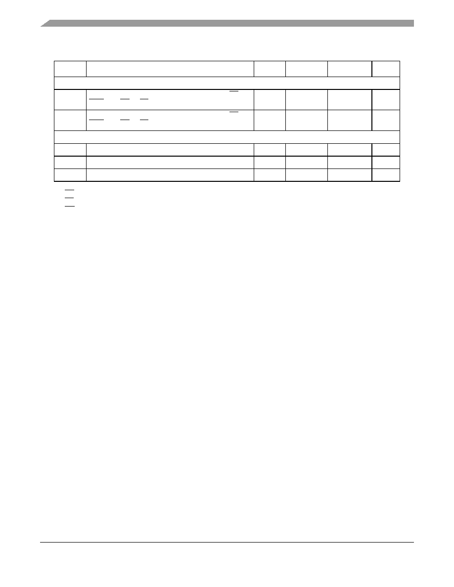
MCF523x Integrated Microprocessor Hardware Specification, Rev. 1.3
Preliminary
Preliminary Electrical Characteristics
Freescale Semiconductor
42
Read/write bus timings listed in
Table 31
are shown in
Figure 11
,
Figure 12
, and
Figure 13
.
Address and Attribute Outputs
B8
CLKOUT high to address (A[23:0]) and control (TS,
TSIZ[1:0], TIP, R/W) valid
t
CHAV
--
9
ns
B9
CLKOUT high to address (A[23:0]) and control (TS,
TSIZ[1:0], TIP, R/W) invalid
t
CHAI
1.5
--
ns
Data Outputs
B11
CLKOUT high to data output (D[31:0]) valid
t
CHDOV
--
9
ns
B12
CLKOUT high to data output (D[31:0]) invalid
t
CHDOI
1.5
--
ns
B13
CLKOUT high to data output (D[31:0]) high impedance
t
CHDOZ
--
9
ns
NOTES:
1
CS transitions after the falling edge of CLKOUT.
2
BS transitions after the falling edge of CLKOUT.
3
OE transitions after the falling edge of CLKOUT.
Table 31. External Bus Output Timing Specifications (continued)
Name
Characteristic
Symbol
Min
Max
Unit
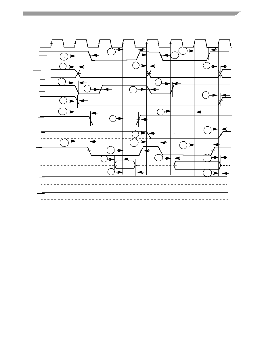
Preliminary Electrical Characteristics
MCF523x Integrated Microprocessor Hardware Specification, Rev. 1.3
Preliminary
Freescale Semiconductor
43
Figure 11. Read/Write (Internally Terminated) SRAM Bus Timing
B12
B13
B8
CLKOUT
CSn
A[23:0]
R/W
BS[3:0]
D[31:0]
TA
(H)
(H)
S0
S2
S3
S1
S4
S5
S0
S1
S2
S3
S4
S5
TEA (H)
B6a
B8
B7a
B6c
B7
B6b
B7
B4
B5
B11
B9
B9
B6b
OE
B0
B7
B9
TS
TIP
B8
B8
B9
B8
B9
TSIZ[1:0]
B7a
B6a
B8
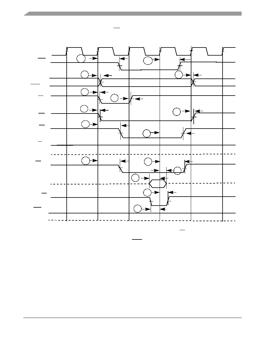
MCF523x Integrated Microprocessor Hardware Specification, Rev. 1.3
Preliminary
Preliminary Electrical Characteristics
Freescale Semiconductor
44
Figure 12
shows a bus cycle terminated by TA showing timings listed in
Table 31
.
Figure 12. SRAM Read Bus Cycle Terminated by TA
Figure 13
shows an SRAM bus cycle terminated by TEA showing timings listed in
Table 31
.
B8
B9
B6a
CLKOUT
CSn
A[23:0]
OE
R/W
BS[3:0]
TA
(H)
S0
S2
S3
S1
S4
S5
S0
S1
TEA
(H)
B8
B7a
B9
B6c
B7
B6b
B7
B2a
B1a
D[31:0]
B4
B5
B8
TS
B9
TIP
TSIZ[1:0]
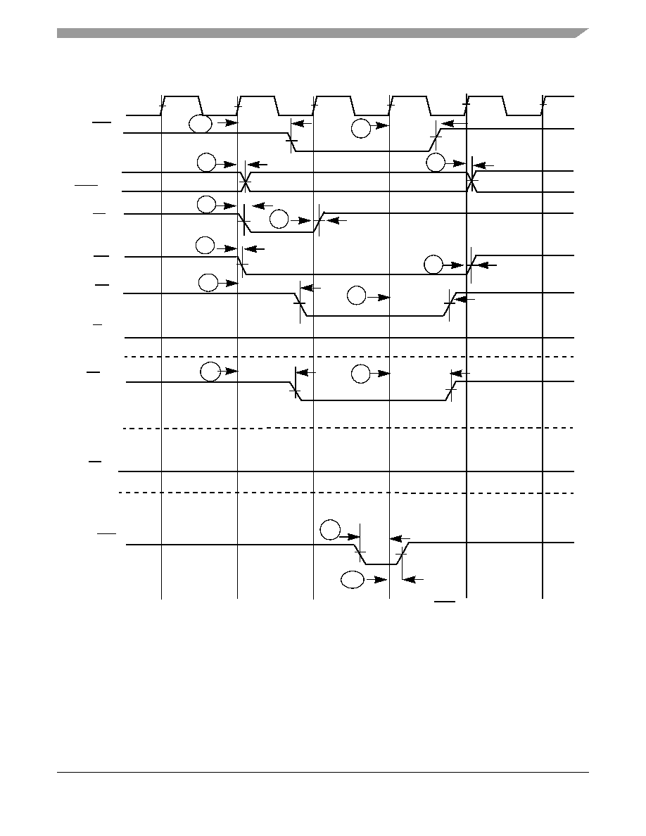
Preliminary Electrical Characteristics
MCF523x Integrated Microprocessor Hardware Specification, Rev. 1.3
Preliminary
Freescale Semiconductor
45
Figure 13. SRAM Read Bus Cycle Terminated by TEA
Figure 14
shows an SDRAM read cycle.
CLKOUT
CSn
A[23:0]
OE
R/W
BS[3:0]
TEA
(H)
S0
S2
S3
S1
S4
S5
S0
S1
TA
(H)
B6a
B8
B7a
B9
B6c
B7
B6b
B7
B2a
B1a
D[31:0]
B8
B9
TS
B9
TIP
B8
TSIZ[1:0]
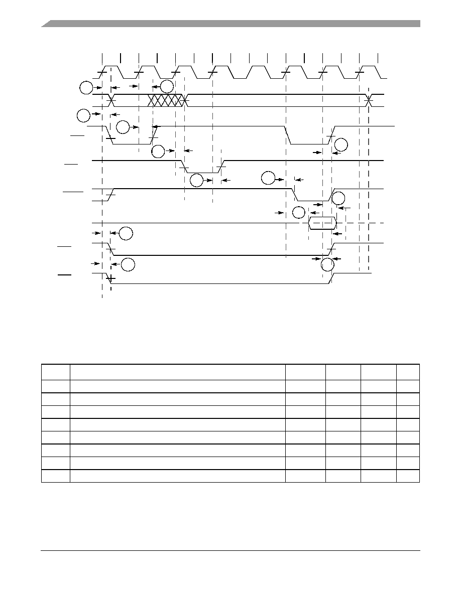
MCF523x Integrated Microprocessor Hardware Specification, Rev. 1.3
Preliminary
Preliminary Electrical Characteristics
Freescale Semiconductor
46
Figure 14. SDRAM Read Cycle
Figure 15
shows an SDRAM write cycle.
Table 32. SDRAM Timing
NUM
Characteristic
Symbol
Min
Max
Unit
D1
CLKOUT high to SDRAM address valid
t
CHDAV
--
9
ns
D2
CLKOUT high to SDRAM control valid
t
CHDCV
--
9
ns
D3
CLKOUT high to SDRAM address invalid
t
CHDAI
1.5
--
ns
D4
CLKOUT high to SDRAM control invalid
t
CHDCI
1.5
--
ns
D5
SDRAM data valid to CLKOUT high
t
DDVCH
4
--
ns
D6
CLKOUT high to SDRAM data invalid
t
CHDDI
1.5
--
ns
D7
1
NOTES:
1
D7 and D8 are for write cycles only.
CLKOUT high to SDRAM data valid
t
CHDDVW
--
9
ns
D8
2
CLKOUT high to SDRAM data invalid
t
CHDDIW
1.5
--
ns
A[23:0]
RAS
D[31:0]
ACTV
NOP
PALL
NOP
RAS[1:0]
READ
Column
SD_CKE
0
SDWE
CAS[3:0]
1
2
3
4
5
6
7
8
9
10
11
12
13
14
15
D1
D2
D4
D6
D5
D4
D4
1
DACR[CASL] = 2
CAS
1
NOP
D4
Row
D3
D2
D2
D2
D2
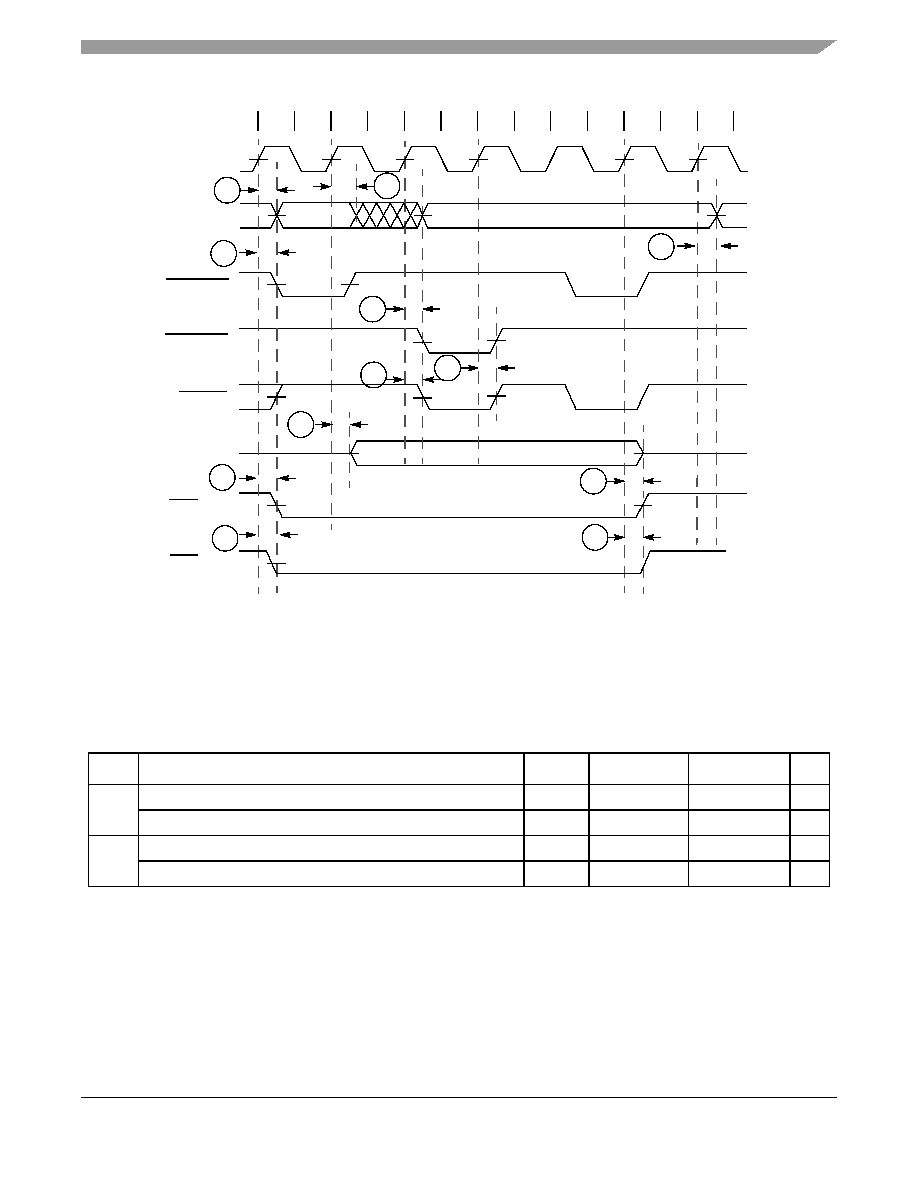
Preliminary Electrical Characteristics
MCF523x Integrated Microprocessor Hardware Specification, Rev. 1.3
Preliminary
Freescale Semiconductor
47
Figure 15. SDRAM Write Cycle
6.7
General Purpose I/O Timing
Table 33. GPIO Timing
1
NOTES:
1
GPIO pins include: INT, ETPU, UART, FlexCAN and Timer pins.
NUM
Characteristic
Symbol
Min
Max
Unit
G1
G2
CLKOUT High to GPIO Output Valid
t
CHPOV
--
10
ns
CLKOUT High to GPIO Output Invalid
t
CHPOI
1.5
--
ns
G3
G4
GPIO Input Valid to CLKOUT High
t
PVCH
9
--
ns
CLKOUT High to GPIO Input Invalid
t
CHPI
1.5
--
ns
A[23:0]
SD_SRAS
SD_SCAS
1
D[31:0]
ACTV
PALL
NOP
RAS[1:0]
WRITE
Row
Column
SD_CKE
SD_WE
CAS[3:0]
D1
D2
D4
D8
0
1
2
3
4
5
6
7
8
9
10
11
12
D7
NOP
1
DACR[CASL] = 2
D4
D3
D2
D2
D2
D4
D2
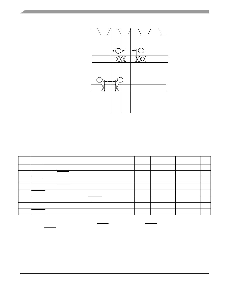
MCF523x Integrated Microprocessor Hardware Specification, Rev. 1.3
Preliminary
Preliminary Electrical Characteristics
Freescale Semiconductor
48
Figure 16. GPIO Timing
6.8
Reset and Configuration Override Timing
Table 34. Reset and Configuration Override Timing
(V
DD
= 2.7 to 3.6 V, V
SS
= 0 V, T
A
= T
L
to T
H
)
1
NOTES:
1
All AC timing is shown with respect to 50% V
DD
levels unless otherwise noted.
NUM
Characteristic
Symbol
Min
Max
Unit
R1
RESET Input valid to CLKOUT High
t
RVCH
9
--
ns
R2
CLKOUT High to RESET Input invalid
t
CHRI
1.5
--
ns
R3
RESET Input valid Time
2
2
During low power STOP, the synchronizers for the RESET input are bypassed and RESET is asserted asynchronously to the
system. Thus, RESET must be held a minimum of 100 ns.
t
RIVT
5
--
t
CYC
R4
CLKOUT High to RSTOUT Valid
t
CHROV
--
10
ns
R5
RSTOUT valid to Config. Overrides valid
t
ROVCV
0
--
ns
R6
Configuration Override Setup Time to RSTOUT invalid
t
COS
20
--
t
CYC
R7
Configuration Override Hold Time after RSTOUT invalid
t
COH
0
--
ns
R8
RSTOUT invalid to Configuration Override High Impedance
t
ROICZ
--
1
t
CYC
G1
CLKOUT
GPIO Outputs
G2
G3
G4
GPIO Inputs
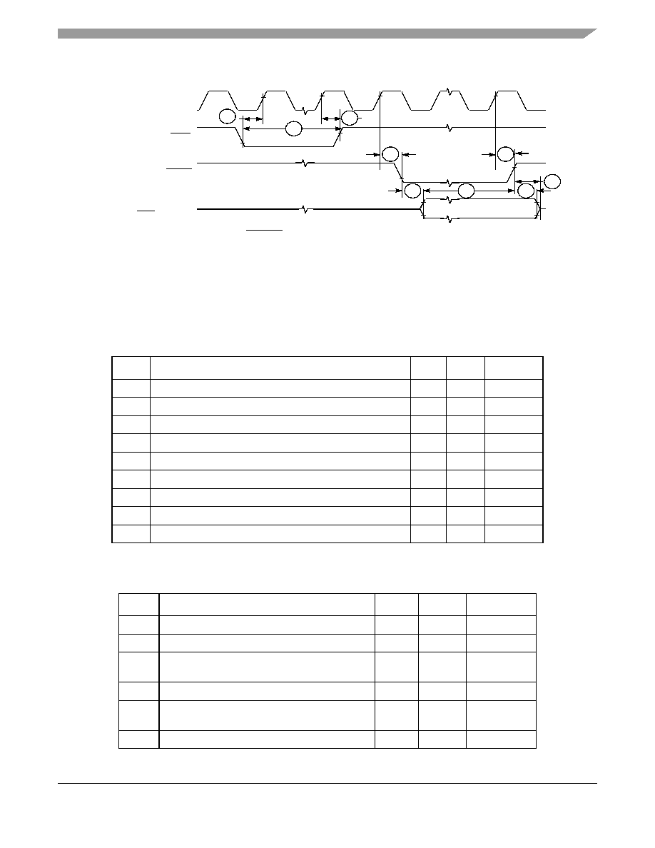
Preliminary Electrical Characteristics
MCF523x Integrated Microprocessor Hardware Specification, Rev. 1.3
Preliminary
Freescale Semiconductor
49
Figure 17. RESET and Configuration Override Timing
* Refer to the Coldfire Integration Module (CIM) section for more information.
6.9
I
2
C Input/Output Timing Specifications
Table 35
lists specifications for the I
2
C input timing parameters shown in
Figure 18
.
Table 36
lists specifications for the I
2
C output timing parameters shown in
Figure 18
.
Table 35. I
2
C Input Timing Specifications between I2C_SCL and I2C_SDA
Num
Characteristic
Min
Max
Units
I1
Start condition hold time
2
--
t
cyc
I2
Clock low period
8
--
t
cyc
I3
I2C_SCL/I2C_SDA rise time (V
IL
= 0.5 V to V
IH
= 2.4 V)
--
1
ms
I4
Data hold time
0
--
ns
I5
I2C_SCL/I2C_SDA fall time (V
IH
= 2.4 V to V
IL
= 0.5 V)
--
1
ms
I6
Clock high time
4
--
t
cyc
I7
Data setup time
0
--
ns
I8
Start condition setup time (for repeated start condition only)
2
--
t
cyc
I9
Stop condition setup time
2
--
t
cyc
Table 36. I
2
C Output Timing Specifications between I2C_SCL and I2C_SDA
Num
Characteristic
Min
Max
Units
I1
1
Start condition hold time
6
--
t
cyc
I2
1
Clock low period
10
--
t
cyc
I3
2
I2C_SCL/I2C_SDA rise time (V
IL
= 0.5 V to
V
IH
= 2.4 V)
--
--
µs
I4
1
Data hold time
7
--
t
cyc
I5
3
I2C_SCL/I2C_SDA fall time (V
IH
= 2.4 V to
V
IL
= 0.5 V)
--
3
ns
I6
1
Clock high time
10
--
t
cyc
R1
R2
CLKOUT
RESET
RSTOUT
R3
R4
R8
R7
R6
R5
Configuration Overrides*:
R4
(RCON, Override pins])
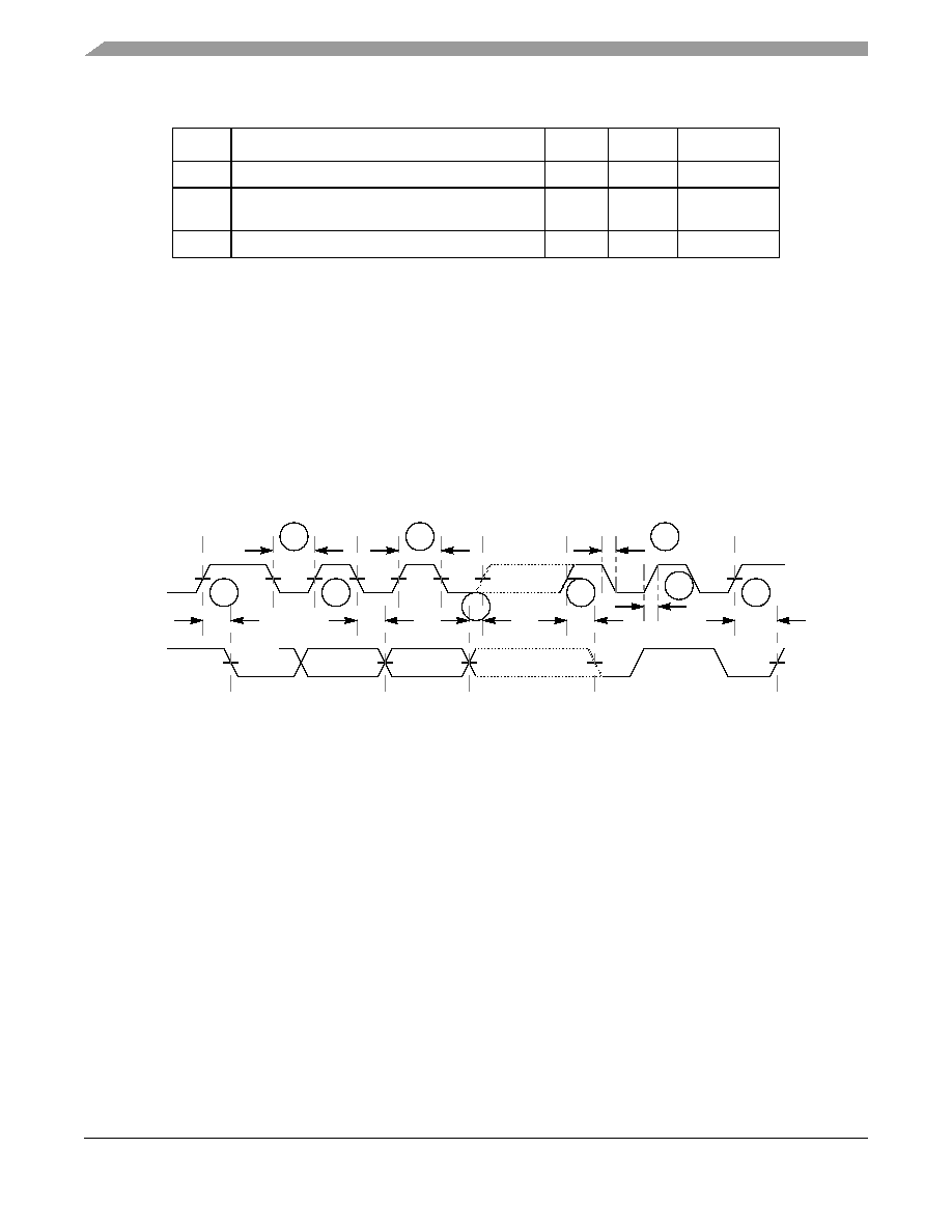
MCF523x Integrated Microprocessor Hardware Specification, Rev. 1.3
Preliminary
Preliminary Electrical Characteristics
Freescale Semiconductor
50
Figure 18
shows timing for the values in
Table 35
and
Table 36
.
Figure 18. I
2
C Input/Output Timings
6.10 Fast Ethernet AC Timing Specifications
MII signals use TTL signal levels compatible with devices operating at either 5.0 V or 3.3 V.
6.10.1 MII Receive Signal Timing (ERXD[3:0], ERXDV, ERXER, and
ERXCLK)
The receiver functions correctly up to a ERXCLK maximum frequency of 25 MHz +1%. There is no
minimum frequency requirement. In addition, the processor clock frequency must exceed twice the
ERXCLK frequency.
Table 37
lists MII receive channel timings.
I7
1
Data setup time
2
--
t
cyc
I8
1
Start condition setup time (for repeated start
condition only)
20
--
t
cyc
I9
1
Stop condition setup time
10
--
t
cyc
NOTES:
1
Note: Output numbers depend on the value programmed into the IFDR; an IFDR
programmed with the maximum frequency (IFDR = 0x20) results in minimum output
timings as shown in
Table 36
. The I
2
C interface is designed to scale the actual data
transition time to move it to the middle of the I2C_SCL low period. The actual position is
affected by the prescale and division values programmed into the IFDR; however, the
numbers given in
Table 36
are minimum values.
2
Because I2C_SCL and I2C_SDA are open-collector-type outputs, which the processor can
only actively drive low, the time I2C_SCL or I2C_SDA take to reach a high level depends on
external signal capacitance and pull-up resistor values.
3
Specified at a nominal 50-pF load.
Table 36. I
2
C Output Timing Specifications between I2C_SCL and I2C_SDA
Num
Characteristic
Min
Max
Units
I2
I6
I1
I4
I7
I8
I9
I5
I3
I2C_SCL
I2C_SDA
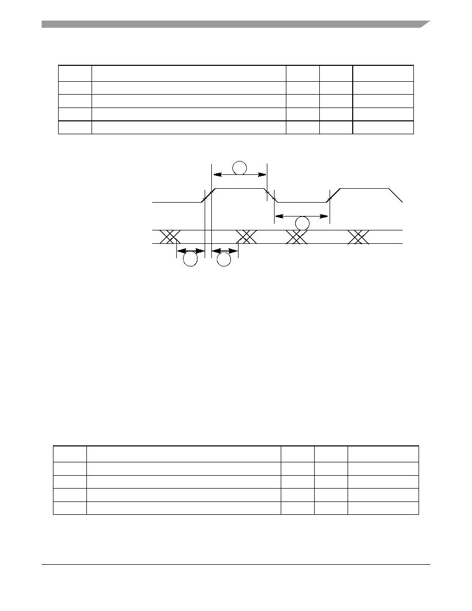
Preliminary Electrical Characteristics
MCF523x Integrated Microprocessor Hardware Specification, Rev. 1.3
Preliminary
Freescale Semiconductor
51
Figure 19
shows MII receive signal timings listed in
Table 37
.
Figure 19. MII Receive Signal Timing Diagram
6.10.2 MII Transmit Signal Timing (ETXD[3:0], ETXEN,
ETXER, ETXCLK)
Table 38
lists MII transmit channel timings.
The transmitter functions correctly up to a ETXCLK maximum frequency of 25 MHz +1%. There is no
minimum frequency requirement. In addition, the processor clock frequency must exceed twice the
ETXCLK frequency.
The transmit outputs (ETXD[3:0], ETXEN, ETXER) can be programmed to transition from either the
rising or falling edge of ETXCLK, and the timing is the same in either case. This options allows the use
of non-compliant MII PHYs.
Refer to the Ethernet chapter for details of this option and how to enable it.
Table 37. MII Receive Signal Timing
Num
Characteristic
Min
Max
Unit
M1
ERXD[3:0], ERXDV, ERXER to ERXCLK setup
5
--
ns
M2
ERXCLK to ERXD[3:0], ERXDV, ERXER hold
5
--
ns
M3
ERXCLK pulse width high
35%
65%
ERXCLK period
M4
ERXCLK pulse width low
35%
65%
ERXCLK period
Table 38. MII Transmit Signal Timing
Num
Characteristic
Min
Max
Unit
M5
ETXCLK to ETXD[3:0], ETXEN, ETXER invalid
5
--
ns
M6
ETXCLK to ETXD[3:0], ETXEN, ETXER valid
--
25
ns
M7
ETXCLK pulse width high
35%
65%
ETXCLK period
M8
ETXCLK pulse width low
35%
65%
ETXCLK period
M1
M2
ERXCLK (input)
ERXD[3:0] (inputs)
ERXDV
ERXER
M3
M4
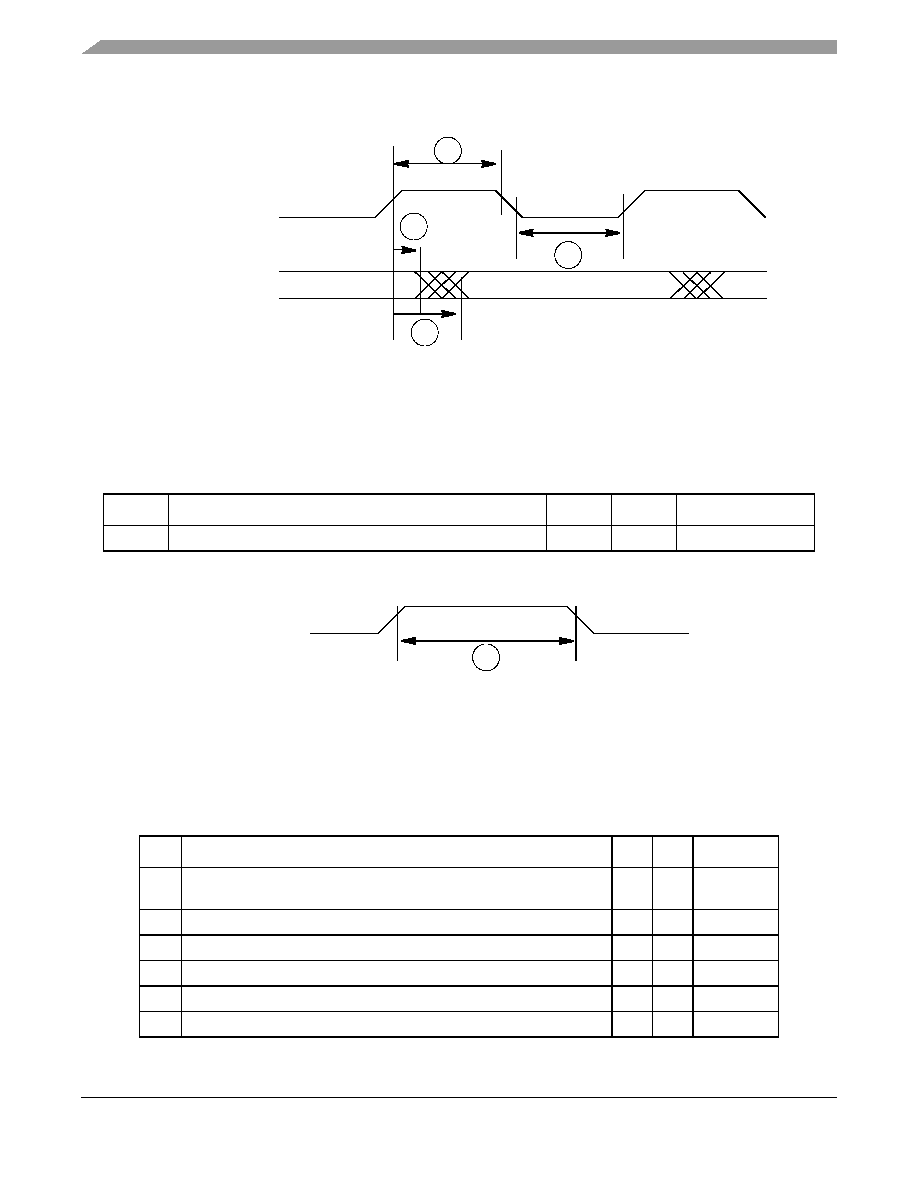
MCF523x Integrated Microprocessor Hardware Specification, Rev. 1.3
Preliminary
Preliminary Electrical Characteristics
Freescale Semiconductor
52
Figure 20
shows MII transmit signal timings listed in
Table 38
.
Figure 20. MII Transmit Signal Timing Diagram
6.10.3 MII Async Inputs Signal Timing (ECRS and ECOL)
Table 39
lists MII asynchronous inputs signal timing.
Figure 21
shows MII asynchronous input timings listed in
Table 39
.
Figure 21. MII Async Inputs Timing Diagram
6.10.4 MII Serial Management Channel Timing (EMDIO and EMDC)
Table 40
lists MII serial management channel timings. The FEC functions correctly with a maximum
MDC frequency of 2.5 MHz.
Table 39. MII Async Inputs Signal Timing
Num
Characteristic
Min
Max
Unit
M9
ECRS, ECOL minimum pulse width
1.5
--
ETXCLK period
Table 40. MII Serial Management Channel Timing
Num
Characteristic
Min
Max
Unit
M10
EMDC falling edge to EMDIO output invalid (minimum propagation
delay)
0
--
ns
M11
EMDC falling edge to EMDIO output valid (max prop delay)
--
25
ns
M12
EMDIO (input) to EMDC rising edge setup
10
--
ns
M13
EMDIO (input) to EMDC rising edge hold
0
--
ns
M14
EMDC pulse width high
40%
60%
MDC period
M15
EMDC pulse width low
40%
60%
MDC period
M6
ETXCLK (input)
ETXD[3:0] (outputs)
ETXEN
ETXER
M5
M7
M8
ECRS, ECOL
M9

Preliminary Electrical Characteristics
MCF523x Integrated Microprocessor Hardware Specification, Rev. 1.3
Preliminary
Freescale Semiconductor
53
Figure 22
shows MII serial management channel timings listed in
Table 40
.
Figure 22. MII Serial Management Channel Timing Diagram
6.11 32-Bit Timer Module AC Timing Specifications
Table 41
lists timer module AC timings.
6.12 QSPI Electrical Specifications
Table 42
lists QSPI timings.
Table 41. Timer Module AC Timing Specifications
Name
Characteristic
0≠66 MHz
Unit
Min
Max
T1
DT0IN / DT1IN / DT2IN / DT3IN cycle time
3
--
t
CYC
T2
DT0IN / DT1IN / DT2IN / DT3IN pulse width
1
--
t
CYC
Table 42. QSPI Modules AC Timing Specifications
Name
Characteristic Min
Max
Unit
QS1
QSPI_CS[1:0] to QSPI_CLK
1
510
tcyc
QS2
QSPI_CLK high to QSPI_DOUT valid.
--
10
ns
QS3
QSPI_CLK high to QSPI_DOUT invalid. (Output hold)
2
--
ns
QS4
QSPI_DIN to QSPI_CLK (Input setup)
9
--
ns
QS5
QSPI_DIN to QSPI_CLK (Input hold)
9
--
ns
M11
EMDC (output)
EMDIO (output)
M12
M13
EMDIO (input)
M10
M14
M15
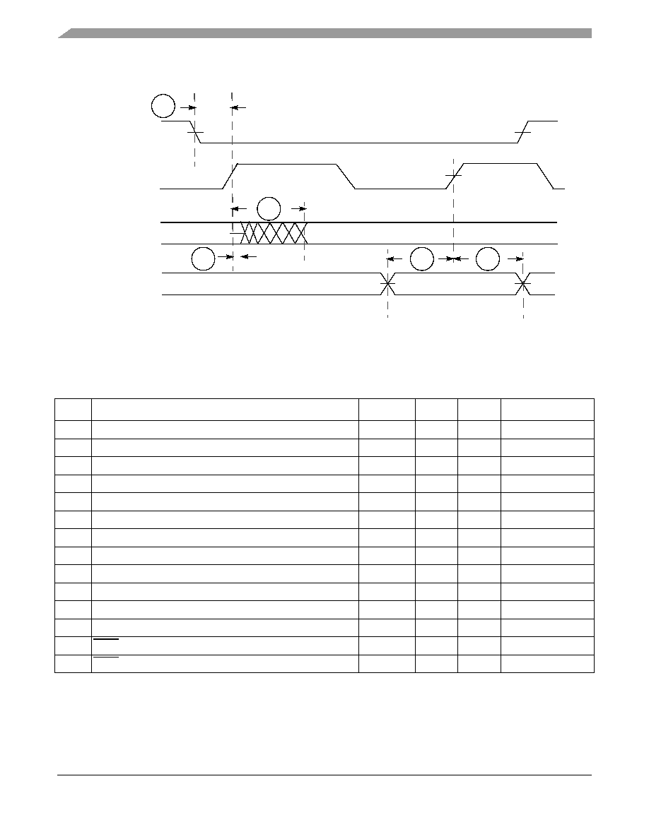
MCF523x Integrated Microprocessor Hardware Specification, Rev. 1.3
Preliminary
Preliminary Electrical Characteristics
Freescale Semiconductor
54
The values in
Table 42
correspond to
Figure 23
.
Figure 23. QSPI Timing
6.13 JTAG and Boundary Scan Timing
Table 43. JTAG and Boundary Scan Timing
Num
Characteristics
1
NOTES:
1
JTAG_EN is expected to be a static signal. Hence, specific timing is not associated with it.
Symbol
Min
Max
Unit
J1
TCLK Frequency of Operation
f
JCYC
DC
1/4
f
sys/2
J2
TCLK Cycle Period
t
JCYC
4
-
t
CYC
J3
TCLK Clock Pulse Width
t
JCW
26
-
ns
J4
TCLK Rise and Fall Times
t
JCRF
0
3
ns
J5
Boundary Scan Input Data Setup Time to TCLK Rise
t
BSDST
4
-
ns
J6
Boundary Scan Input Data Hold Time after TCLK Rise
t
BSDHT
26
-
ns
J7
TCLK Low to Boundary Scan Output Data Valid
t
BSDV
0
33
ns
J8
TCLK Low to Boundary Scan Output High Z
t
BSDZ
0
33
ns
J9
TMS, TDI Input Data Setup Time to TCLK Rise
t
TAPBST
4
-
ns
J10
TMS, TDI Input Data Hold Time after TCLK Rise
t
TAPBHT
10
-
ns
J11
TCLK Low to TDO Data Valid
t
TDODV
0
26
ns
J12
TCLK Low to TDO High Z
t
TDODZ
0
8
ns
J13
TRST Assert Time
t
TRSTAT
100
-
ns
J14
TRST Setup Time (Negation) to TCLK High
t
TRSTST
10
-
ns
QSPI_CS[1:0]
QSPI_CLK
QSPI_DOUT
QS5
QS1
QSPI_DIN
QS3
QS4
QS2
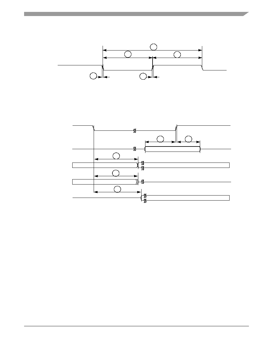
Preliminary Electrical Characteristics
MCF523x Integrated Microprocessor Hardware Specification, Rev. 1.3
Preliminary
Freescale Semiconductor
55
Figure 24. Test Clock Input Timing
Figure 25. Boundary Scan (JTAG) Timing
TCLK
V
IL
V
IH
J3
J3
J4
J4
J2
(input)
Input Data Valid
Output Data Valid
Output Data Valid
TCLK
Data Inputs
Data Outputs
Data Outputs
Data Outputs
V
IL
V
IH
J5
J6
J7
J8
J7
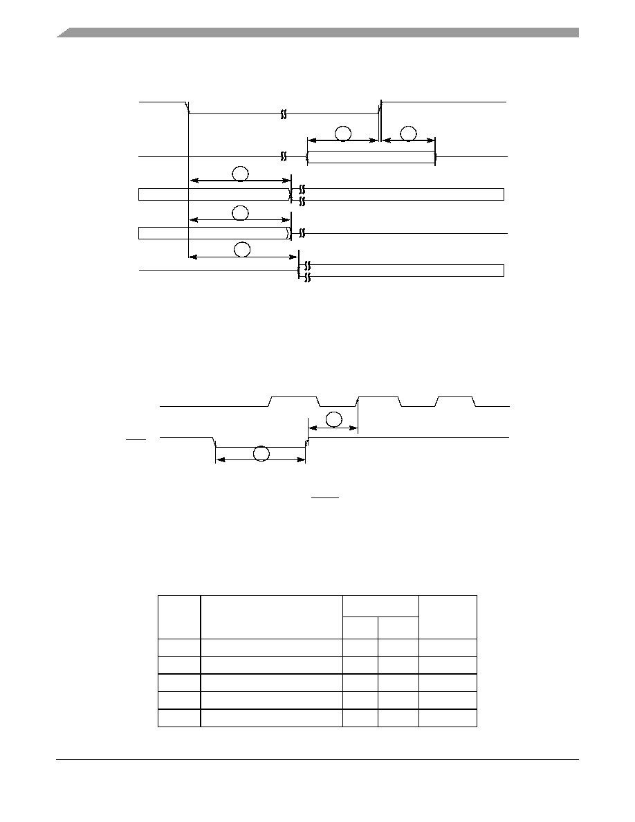
MCF523x Integrated Microprocessor Hardware Specification, Rev. 1.3
Preliminary
Preliminary Electrical Characteristics
Freescale Semiconductor
56
Figure 26. Test Access Port Timing
Figure 27. TRST Timing
6.14 Debug AC Timing Specifications
Table 44
lists specifications for the debug AC timing parameters shown in
Figure 29
.
Table 44. Debug AC Timing Specification
Num
Characteristic
150 MHz
Units
Min
Max
DE0
PSTCLK cycle time
0.5
t
cyc
DE1
PST valid to PSTCLK high
4
ns
DE2
PSTCLK high to PST invalid
1.5
ns
DE3
DSCLK cycle time
5
t
cyc
DE4
DSI valid to DSCLK high
1
t
cyc
Input Data Valid
Output Data Valid
Output Data Valid
TCLK
TDI
TDO
TDO
TDO
TMS
V
IL
V
IH
J9
J10
J11
J12
J11
TCLK
TRST
J14
J13
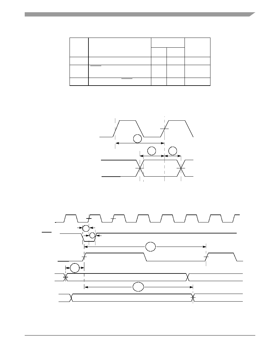
Preliminary Electrical Characteristics
MCF523x Integrated Microprocessor Hardware Specification, Rev. 1.3
Preliminary
Freescale Semiconductor
57
Figure 28
shows real-time trace timing for the values in
Table 44
.
Figure 28. Real-Time Trace AC Timing
Figure 29
shows BDM serial port AC timing for the values in
Table 44
.
Figure 29. BDM Serial Port AC Timing
DE5
1
DSCLK high to DSO invalid
4
t
cyc
DE6
BKPT input data setup time to
CLKOUT Rise
4
ns
DE7
CLKOUT high to BKPT high Z
0
10
ns
NOTES:
1
DSCLK and DSI are synchronized internally. D4 is measured from the
synchronized DSCLK input relative to the rising edge of CLKOUT.
Table 44. Debug AC Timing Specification
Num
Characteristic
150 MHz
Units
Min
Max
PSTCLK
PST[3:0]
DE2
DE1
DDATA[3:0]
DE0
DSI
DSO
Current
Next
CLKOUT
Past
Current
DSCLK
DE3
DE4
DE5
BKPT
DE6
DE7
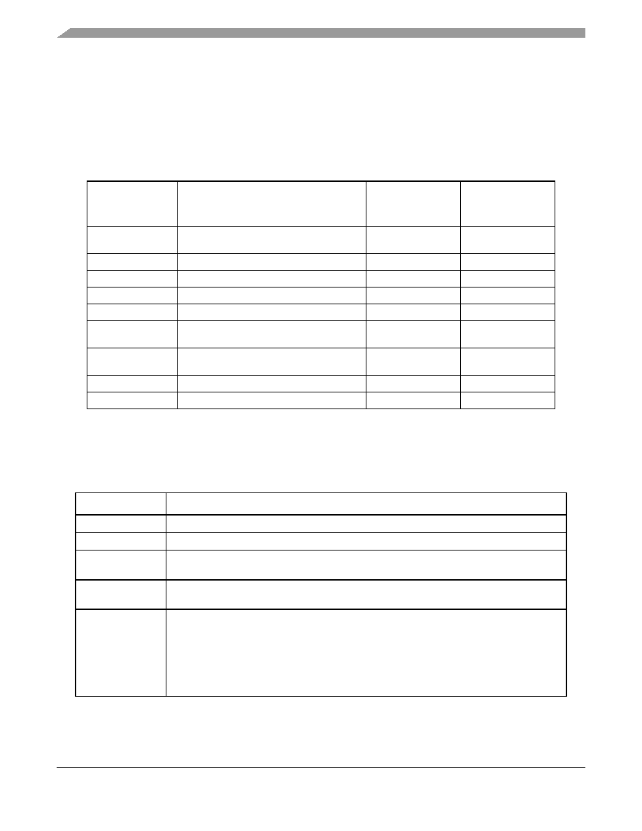
MCF523x Integrated Microprocessor Hardware Specification, Rev. 1.3
Preliminary
Documentation
Freescale Semiconductor
58
7
Documentation
Table 46
lists the documents that provide a complete description of the MCF523x and their development
support tools. Documentation is available from a local Freescale distributor, a Freescale semiconductor
sales office, the Freescale Literature Distribution Center, or through the Freescale world-wide web address
at
http://www.freescale.com
.
7.1
Document Revision History
Table 46
provides a revision history for this document.
Table 45. MCF523x Documentation
Freescale
Document
Number
Title
Revision
Status
MCF5235EC
MCF5235 RISC Microprocessor Hardware
Specifications
Rev. 1.3
This document
MCF5235RM
MCF523x Reference Manual
1
Available
MCF5235PB
MCF523x Product Brief
0
Available
MCF523xFS
MCF523x Fact Sheet
--
In Process
eTPURM/D
eTPU User Manual
0
Available
CFPRODFACT/D
The ColdFire Family of 32-Bit Microprocessors
Family Overview and Technology Roadmap
0
Available under
NDA
MCF5xxxWP
MCF5xxxWP WHITE PAPER: Motorola ColdFire
VL RISC Processors
0
Available under
NDA
MAPBGAPP
MAPBGA 4-Layer Example
0
Available
CFPRM/D
ColdFire Family Programmer's Reference Manual
2
Available
Table 46. Document Revision History
Rev. No.
Substantive Change(s)
0
Preliminary release.
1
-Updated Signal List table
1.1
-Removed duplicate information in the module description sections. The information is all in the
Signals Description Table.
1.2
-Corrected
Figure 8
pin 81. VDD instead of VSS
-Changed instances of Motorola to Freescale
1.3
-Removed detailed signal description section. This information can be found in the MCF5235RM
Chapter 2.
-Removed detailed feature list. This information can be found in the MCF5235RM Chapter 1.
-Corrected
Figure 2
pin F10. VSS instead of VDD. Change made in
Table 2
as well.
-Corrected
Figure 8
pin 81. OVDD instead of VDD. Change made in
Table 2
as well.
-Cleaned up many inconsistencies within the pinout figure signal names
-Corrected document IDs in
Table 45

THIS PAGE INTENTIONALLY LEFT BLANK
MCF523x Integrated Microprocessor Hardware Specification, Rev. 1.3
Preliminary
Freescale Semiconductor
59

MCF5235EC
Rev. 1.3, 10/2004
HOW TO REACH US:
USA/Europe/Locations not listed:
Freescale Semiconductor Literature Distribution
P.O. Box 5405, Denver, Colorado 80217
1-800-521-6274 or 480-768-2130
Japan:
Freescale Semiconductor Japan Ltd.
Technical Information Center
3-20-1, Minami-Azabu, Minato-ku
Tokyo 106-8573, Japan
81-3-3440-3569
Asia/Pacific:
Freescale Semiconductor H.K. Ltd.
2 Dai King Street
Tai Po Industrial Estate
Tai Po, N.T. Hong Kong
852-26668334
Learn More:
For more information about Freescale
Semiconductor products, please visit
http://www.freescale.com
Information in this document is provided solely to enable system and software implementers to use
Freescale Semiconductor products. There are no express or implied copyright licenses granted
hereunder to design or fabricate any integrated circuits or integrated circuits based on the information
in this document.
Freescale Semiconductor reserves the right to make changes without further notice to any products
herein. Freescale Semiconductor makes no warranty, representation or guarantee regarding the
suitability of its products for any particular purpose, nor does Freescale Semiconductor assume any
liability arising out of the application or use of any product or circuit, and specifically disclaims any
and all liability, including without limitation consequential or incidental damages. "Typical" parameters
which may be provided in Freescale Semiconductor data sheets and/or specifications can and do
vary in different applications and actual performance may vary over time. All operating parameters,
including "Typicals" must be validated for each customer application by customer's technical experts.
Freescale Semiconductor does not convey any license under its patent rights nor the rights of others.
Freescale Semiconductor products are not designed, intended, or authorized for use as components
in systems intended for surgical implant into the body, or other applications intended to support or
sustain life, or for any other application in which the failure of the Freescale Semiconductor product
could create a situation where personal injury or death may occur. Should Buyer purchase or use
Freescale Semiconductor products for any such unintended or unauthorized application, Buyer shall
indemnify and hold Freescale Semiconductor and its officers, employees, subsidiaries, affiliates, and
distributors harmless against all claims, costs, damages, and expenses, and reasonable attorney
fees arising out of, directly or indirectly, any claim of personal injury or death associated with such
unintended or unauthorized use, even if such claim alleges that Freescale Semiconductor was
negligent regarding the design or manufacture of the part.
FreescaleTM and the Freescale logo are trademarks of Freescale Semiconductor, Inc. All other
product or service names are the property of their respective owners.
© Freescale Semiconductor, Inc. 2004.
∑ Preliminary