 | –≠–ª–µ–∫—Ç—Ä–æ–Ω–Ω—ã–π –∫–æ–º–ø–æ–Ω–µ–Ω—Ç: MCF5483 | –°–∫–∞—á–∞—Ç—å:  PDF PDF  ZIP ZIP |

© Freescale Semiconductor, Inc., 2004. All rights reserved.
Freescale Semiconductor
Data Sheet
MCF5485EC
Rev. 2.1, 12/2004
Table of Contents
This chapter contains electrical specification tables and
reference timing diagrams for the MCF548x
microprocessor. This section contains detailed
information on power considerations, DC/AC electrical
characteristics, and AC timing specifications of the
MCF548x.
NOTE
The parameters specified
in this MPU document
supersede any values
found in the module
specifications.
1
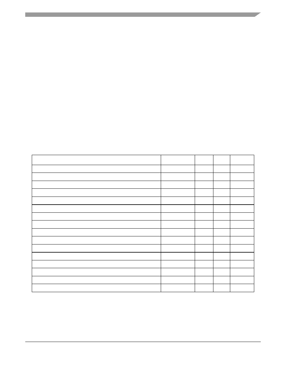
Maximum Ratings
Table 1
lists maximum and minimum ratings for supply
and operating voltages and storage temperature.
Operating outside of these ranges may cause erratic
behavior or damage to the processor.
1
Maximum Ratings................................................ 1
2
Thermal Characteristics ......................................2
3
DC Electrical Specifications ................................ 3
4
Supply Voltage Sequencing and Separation
Cautions .............................................................. 5
5
Output Driver Capability and Loading ................. 6
6
PLL Timing Specifications ................................... 7
7
Reset Timing Specifications ................................ 8
8
FlexBus................................................................ 9
9
SDRAM Bus ...................................................... 11
10
PCI Bus ............................................................. 17
11
Fast Ethernet AC Timing Specifications ............ 18
12
General Timing Specifications........................... 21
13
I
2
C Input/Output Timing Specifications ............. 21
14
JTAG and Boundary Scan Timing ..................... 23
15
DSPI Electrical Specifications ........................... 26
16
Timer Module AC Timing Specifications............ 26
MCF548x Integrated
Microprocessor Electrical
Characteristics
Applies to the MCF5480, MCF5481, MCF5482, MCF5483,
MCF5484, and MCF5485

MCF548x Integrated Microprocessor Electrical Characteristics, Rev. 2.1
Thermal Characteristics
Freescale Semiconductor
2
2
Thermal Characteristics
2.1
Operating Temperatures
Table 2
lists junction and ambient operating temperatures.
2.2
Thermal Resistance
Table 3
lists thermal resistance values.
Table 1. Absolute Maximum Ratings
Rating
Symbol
Value
Units
External (I/O pads) supply voltage (3.3-V power pins)
EV
DD
≠0.3 to +4.0
V
Internal logic supply voltage
IV
DD
≠0.5 to +2.0
V
Memory (I/O pads) supply voltage (2.5-V power pins)
SD V
DD
≠0.3 to +4.0 SDR Memory
≠0.3 to +2.8 DDR Memory
V
PLL supply voltage
PLL V
DD
≠0.5 to +2.0
V
Internal logic supply voltage, input voltage level
V
in
≠0.5 to +3.6
V
Storage temperature range
T
stg
≠55 to +150
o
C
Table 2. Operating Temperatures
Characteristic
Symbol
Value
Units
Maximum operating junction temperature
T
j
105
o
C
Maximum operating ambient temperature
T
Amax
<85
1
NOTES:
1
This published maximum operating ambient temperature should be used only as a system design guideline. All
device operating parameters are guaranteed only when the junction temperature lies within the specified range.
o
C
Minimum operating ambient temperature
T
Amin
≠ 40
o
C
Table 3. Thermal Resistance
Characteristic
Symbol
Value
Unit
324 pin TEPBGA -- Junction to ambient, natural
convection
Four layer board (2s2p)
JMA
22≠24
1,2
∞C/W
388 pin TEPBGA -- Junction to ambient, natural
convection
Four layer board (2s2p)
JMA
20≠22
1
,
2
∞C/W
Junction to ambient (@200 ft/min)
Four layer board (2s2p)
JMA
23
1
,
2
∞C/W
Junction to board
JB
15
3
∞C/W
Junction to case
JC
10
4
∞C/W
Junction to top of package
Natural convection
jt
2
1
,5
∞C/W
DC Electrical Specifications
MCF548x Integrated Microprocessor Electrical Characteristics, Rev. 2.1
Freescale Semiconductor
3
3
DC Electrical Specifications
Table 4
lists DC electrical operating temperatures. This table is based on an operating voltage of
EV
DD
= 3.3 V
DC
± 0.3 V
DC
and IV
DD
of 1.5 ± 0.07 V
DC
.
NOTES:
1
JA
and
jt
parameters are simulated in accordance with EIA/JESD Standard 51-2 for natural convection.
Freescale recommends the use of
JA
and power dissipation specifications in the system design to prevent device
junction temperatures from exceeding the rated specification. System designers should be aware that device
junction temperatures can be significantly influenced by board layout and surrounding devices. Conformance to the
device junction temperature specification can be verified by physical measurement in the customer's system using
the
jt
parameter, the device power dissipation, and the method described in EIA/JESD Standard 51-2.
2
Per JEDEC JESD51-6 with the board horizontal.
3
Thermal resistance between the die and the printed circuit board per JEDEC JESD51-8. Board temperature is
measured on the top surface of the board near the package.
4
Thermal resistance between the die and the case top surface as measured by the cold plate method (MIL
SPEC-883 Method 1012.1).
5
Thermal characterization parameter indicating the temperature difference between package top and the junction
temperature per JEDEC JESD51-2. When Greek letters are not available, the thermal characterization parameter
is written as Psi-JT.
Table 4.
DC Electrical Specifications
Characteristic
Symbol
Min
Max
Units
External (I/O pads) operation voltage range
EV
DD
3.0
3.6
V
Memory (I/O pads) operation voltage range (DDR Memory)
SD V
DD
2.30
2.70
V
Internal logic operation voltage range
1
NOTES:
1
IV
DD
and PLL V
DD
should be at the same voltage. PLL V
DD
should have a filtered input. Please see
Figure 1
for an
example circuit. Note: There are three PLL V
DD
inputs. A filter circuit should used on each PLL V
DD
input.
IV
DD
1.43
1.58
V
PLL Analog operation voltage range
1
PLL V
DD
1.43
1.58
V
USB oscillator operation voltage range
USB_OSV
DD
3.0
3.6
V
USB digital logic operation voltage range
USBV
DD
3.0
3.6
V
USB PHY operation voltage range
USB_PHYV
DD
3.0
3.6
V
USB oscillator analog operation voltage range
USB_OSCAV
DD
1.43
1.58
V
USB PLL operation voltage range
USB_PLLV
DD
1.43
1.58
V
Input high voltage SSTL 3.3V (SDR DRAM)
V
IH
2.0
3.6
V
Input low voltage SSTL 3.3V (SDR DRAM)
V
IL
≠0.5
0.8
V
Input high voltage SSTL 2.5V (DDR DRAM)
V
IH
2.0
2.8
V
Input low voltage SSTL 2.5V (DDR DRAM)
V
IL
≠0.5
0.8
V
Output high voltage I
OH
= 8 mA, 16 mA,24 mA
V
OH
2.4
-- V
Output low voltage I
OL
= 8 mA, 16 mA,24 mA
5
V
OL
--
0.5
V
Capacitance
2
, V
in
= 0 V, f = 1 MHz
2
Capacitance C
IN
is periodically sampled rather than 100% tested.
C
IN
--
TBD
pF
MCF548x Integrated Microprocessor Electrical Characteristics, Rev. 2.1
DC Electrical Specifications
Freescale Semiconductor
4
3.1
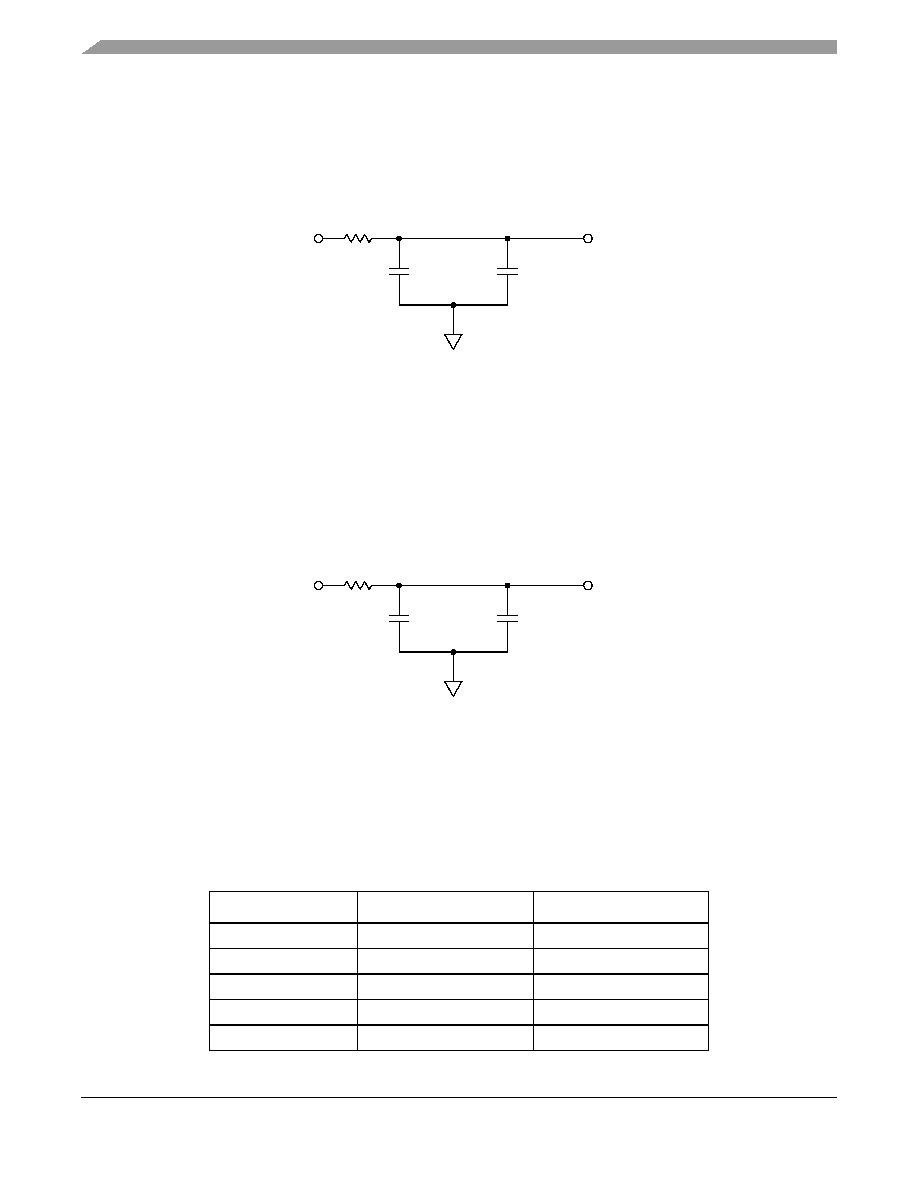
PLL Power Filtering
To further enhance noise isolation, an external filter is strongly recommended for PLL analog V
DD
pins.
The filter shown in
Figure 1
should be connected between the board V
DD
and the PLL V
DD
pins. The
resistor and capacitors should be placed as close to the dedicated PLL V
DD
pin as possible.
Figure 1. System PLL V
DD
Power Filter
3.2
USB Power Filtering
To minimize noise, a external filters are required for each of the USB power pins. The filter shown in
Figure 2
should be connected between the board EV
DD
or IV
DD
and each of the USB V
DD
pins. The
resistor and capacitors should be placed as close to the dedicated USB V
DD
pin as possible. A separate
filter circuit should be included for each USB V
DD
pin, a total of five circuits.
Figure 2. USB V
DD
Power Filter
NOTE
In addition to the above filter circuitry, a 0.01 F capacitor is also
recommended in parallel with those shown.
Table 5
lists the resistor values and supply voltages to be used in the circuit for each of the USB V
DD
pins.
Table 5. USB Filter Circuit Values
USB V
DD
Pin
Nominal Voltage
Resistor Value (R)
USB_OSCVDD
3.3V
0
USBVDD
3.3V
0
USB_PHYVDD
3.3V
0
USB_OSCAVDD
1.5V
0
USB_PLLVDD
1.5V
10
Board V
DD
10 W
0.1 µF
PLL V
DD
Pin
10 µF
GND
Board EV
DD
/IV
DD
R
0.1 µF
USB V
DD
Pin
10 µF
GND
Supply Voltage Sequencing and Separation Cautions
MCF548x Integrated Microprocessor Electrical Characteristics, Rev. 2.1
Freescale Semiconductor
5
4
Supply Voltage Sequencing and Separation
Cautions
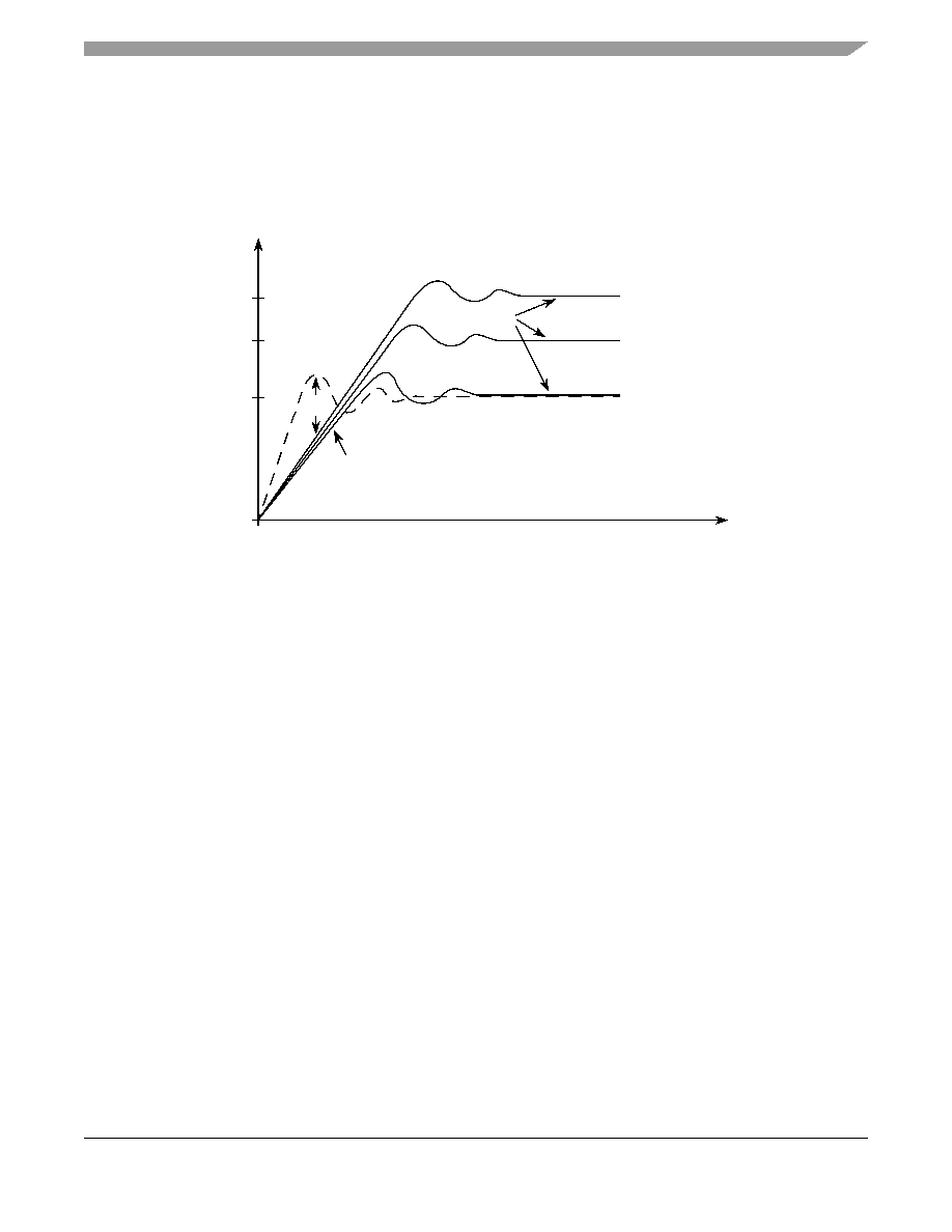
Figure 3
shows situations in sequencing the I/O V
DD
(EV
DD
), SDRAM V
DD
(SD V
DD
), PLL V
DD
(PLL
V
DD
), and Core V
DD
(IV
DD
).
Figure 3. Supply Voltage Sequencing and Separation Cautions
The relationship between SD V
DD
and EV
DD
is non-critical during power-up and power-down sequences.
Both SD V
DD
(2.5V or 3.3V) and EV
DD
are specified relative to IV
DD
.
4.1
Power Up Sequence
If EV
DD
/SD V
DD
are powered up with the IV
DD
at 0V, then the sense circuits in the I/O pads will cause
all pad output drivers connected to the EV
DD
/SD V
DD
to be in a high impedance state. There is no limit
on how long after EV
DD
/SD V
DD
powers up before IV
DD
must power up. IV
DD
should not lead the EV
DD
,
SD V
DD
or PLL V
DD
by more than 0.4V during power ramp up, or there will be high current in the internal
ESD protection diodes. The rise times on the power supplies should be slower than 1 microsecond to avoid
turning on the internal ESD protection clamp diodes.
EV
DD
, SD V
DD
(3.3V)
SD V
DD
(2.5V)
IV
DD
, PLL V
DD
Supplies Stable
2
1
3.3V
2.5V
1.5V
0
Time
NOTES:
IV
DD
should not exceed EV
DD
, SD V
DD
or PLL V
DD
by more than
0.4V at any time, including power-up.
Recommended that IV
DD
/PLL V
DD
should track EV
DD
/SD V
DD
up to
0.9V, then separate for completion of ramps.
Input voltage must not be greater than the supply voltage (EV
DD
, SD V
DD
,
IV
DD
, or PLL V
DD
) by more than 0.5V at any time, including during power-up.
Use 1 microsecond or slower rise time for all supplies.
1.
2.
3.
4.
DC P
o
w
e
r Supp
ly V
o
ltage
MCF548x Integrated Microprocessor Electrical Characteristics, Rev. 2.1
Output Driver Capability and Loading
Freescale Semiconductor
6
The recommended power up sequence is as follows:
1. Use 1 microsecond or slower rise time for all supplies.
2. IV
DD
/PLL V
DD
and EV
DD
/SD V
DD
should track up to 0.9V, then separate for the completion of
ramps with EV
DD
/SD V
DD
going to the higher external voltages. One way to accomplish this is to
use a low drop-out voltage regulator.
4.2
Power Down Sequence
If IV
DD
PLL V
DD
are powered down first, then sense circuits in the I/O pads will cause all output drivers
to be in a high impedance state. There is no limit on how long after IV
DD
and PLL V
DD
power down before
EV
DD
or SD V
DD
must power down. IV
DD
should not lag EV
DD
, SD V
DD
, or PLL V
DD
going low by
more than 0.4V during power down or there will be undesired high current in the ESD protection diodes.
There are no requirements for the fall times of the power supplies.
The recommended power down sequence is as follows:
1. Drop IV
DD
/PLL V
DD
to 0V
2. Drop EV
DD
/SD V
DD
supplies
5
Output Driver Capability and Loading
Table 6
lists values for drive capability and output loading.
Table 6. I/O Driver Capability
Signal
Drive
Capability
Output
Load (C
L
)
SDRAMC (SDADDR[12:0], SDDATA[31:0], RAS, CAS, SDDM[3:0],
SDWE, SDBA[1:0]
24 mA
15 pF
SDRAMC DQS and clocks (SDDQS[3:0], SDRDQS, SDCLK[1:0],
SDCLK[1:0], SDCKE)
24 mA
15 pF
SDRAMC chip selects (SDCS[3:0])
24 mA
15 pF
FlexBus (AD[31:0], FBCS[5:0], ALE, R/W, BE/BWE[3:0], OE)
16 mA
20 pF
FEC (EnMDIO, EnMDC, EnTXEN, EnTXD[3:0], EnTXER
8 mA
15 pF
Timer (TOUT[3:0])
8 mA
50 pF
FlexCAN (CANTX)
8 mA
30 pF
DACK[1:0]
8 mA
30 pF
PSC (PSCnTXD[3:0], PSCnRTS/PSCnFSYNC,
8 mA
30 pF
DSPI (DSPISOUT, DSPICS0/SS, DSPICS[2:3], DSPICS5/PCSS)
24 mA
50 pF
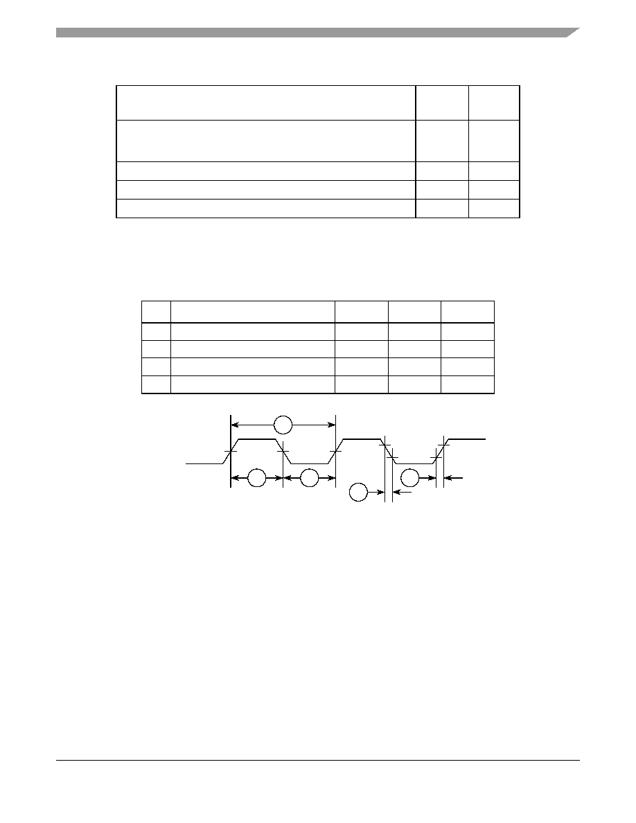
PLL Timing Specifications
MCF548x Integrated Microprocessor Electrical Characteristics, Rev. 2.1
Freescale Semiconductor
7
6
PLL Timing Specifications
The specifications in
Table 7
are for the CLKIN pin.
Figure 4. Input Clock Timing Diagram
PCI (PCIAD[31:0], PCIBG[4:1], PCIBG0/PCIREQOUT, PCIDEVSEL,
PCICXBE[3:0], PCIFRM, PCIPERR, PCIRESET, PCISERR, PCISTOP,
PCIPAR, PCITRDY, PCIIRDY
16 mA
50 pF
I2C (SCL, SDA)
8 mA
50 pF
BDM (PSTCLK, PSTDDATA[7:0], DSO/TDO,
8 mA
25 pF
RSTO
8 mA
50 pF
Table 7. Clock Timing Specification
Num Characteristic
Min
Max
Units
C1
Cycle time
15.15
33.3
ns
C2
Rise time (20% of Vdd to 80% of vdd)
--
2
ns
C3
Fall time (80% of Vdd to 20% of Vdd)
--
2
ns
C4
Duty cycle (at 50% of Vdd)
40
60
%
Table 6. I/O Driver Capability (continued)
Signal
Drive
Capability
Output
Load (C
L
)
CLKIN
C4
C1
C4
C2
C3

MCF548x Integrated Microprocessor Electrical Characteristics, Rev. 2.1
Reset Timing Specifications
Freescale Semiconductor
8
Figure 5
correlates CLKIN, internal bus, and core clock frequencies for the 1x≠4x multipliers.
Figure 5. CLKIN, Internal Bus, and Core Clock Ratios
7
Reset Timing Specifications
Table 9
lists specifications for the reset timing parameters shown in
Figure 6
Figure 6
shows reset timing for the values in
Table 9
.
Table 8. MCF548X Divide Ratio Encodings
AD[12:8]
1
NOTES:
1
All other values of AD[12:8] are reserved.
Clock
Ratio
CLKIN--PCI and FlexBus
Frequency Range (MHz)
Internal XLB, SDRAM
Bus, and PSTCLK Frequency
Range (MHz)
Core Frequency Range
(MHz)
00011
1:2
41.6≠50.0
83.33≠100
166.66≠200
00101
1:2
25.0≠41.5
50.0≠83.0
2
2
Note that DDR memories typically have a minimum speed of 83 MHz. Some vendors specify down to 75 MHz.
Check with memory component specifications to verify.
100.0≠166.66
01111
1:4
25
100
200
Table 9. Reset Timing Specification
Num
Characteristic
66 MHz CLKIN
Units
Min
Max
R1
1
NOTES:
1
RSTI and FlexBus data lines are synchronized internally. Setup and hold
times must be met only if recognition on a particular clock is required.
Valid to CLKIN (setup)
8
--
nS
R2
CLKIN to invalid (hold)
1.0
--
nS
R3
RSTI to invalid (hold)
1.0
--
nS
25 40 50 60 70
70 80 90 100 110 120 130 140 150 160 170 180 190 200
60
25.0
50.0
100.0
CLKIN (MHz)
Core Clock (MHz)
Core Clock
CLKIN
200.0
40 50 60 70 80 90 100
30
50.0
100.0
Internal Clock
Internal Clock (MHz)
2x
2x
25.0
200.0
2x
4x
100.0
FlexBus
MCF548x Integrated Microprocessor Electrical Characteristics, Rev. 2.1
Freescale Semiconductor
9
Figure 6. Reset Timing
8
FlexBus
A multi-function external bus interface called FlexBus is provided on the MCF5482 with basic
functionality to interface to slave-only devices up to a maximum bus frequency of 66 MHz. It can be
directly connected to asynchronous or synchronous devices such as external boot ROMs, flash memories,
gate-array logic, or other simple target (slave) devices with little or no additional circuitry. For
asynchronous devices, a simple chip-select based interface can be used. The FlexBus interface has six
general purpose chip-selects (FBCS[5:0]). Chip-select FBCS0 can be dedicated to boot ROM access and
can be programmed to be byte (8 bits), word (16 bits), or longword (32 bits) wide. Control signal timing
is compatible with common ROM / flash memories.
8.1
FlexBus AC Timing Characteristics
The following timing numbers indicate when data will be latched or driven onto the external bus, relative
to the system clock.
Table 10. FlexBus AC Timing Specifications
Num
Characteristic
Min
Max
Unit
Notes
Frequency of Operation
25
66
Mhz
1
FB1
Clock Period (CLKIN)
15.15
33.33
ns
2
FB2
Address, Data, and Control Output Valid (AD[31:0], FBCS[5:0],
R/W, ALE, TSIZ[1:0], BE/BWE[3:0], OE, and TBST)
--
7.0
ns
3
FB3
Address, Data, and Control Output Hold ((AD[31:0], FBCS[5:0],
R/W, ALE, TSIZ[1:0], BE/BWE[3:0], OE, and TBST)
1
--
ns
3
, 4
FB4
Data Input Setup
3.5
--
ns
FB5
Data Input Hold
0
--
ns
CLKIN
R1
R3
R2
R1
RSTI
Mode Select
FlexBus
NOTE:
Mode selects are registered on the rising clock edge before
the cycle in which RSTI is recognized as being negated.
MCF548x Integrated Microprocessor Electrical Characteristics, Rev. 2.1
FlexBus
Freescale Semiconductor
10
Figure 7. FlexBus Read Timing
FB6
Transfer Acknowledge (TA) Input Setup
4
--
ns
FB7
Transfer Acknowledge (TA) Input Hold
0
--
ns
FB8
Address Output Valid (PCIAD[31:0])
--
7.0
ns
5
FB9
Address Output Hold (PCIAD[31:0])
0
--
ns
5
NOTES:
1
The frequency of operation is the same as the PCI frequency of operation. The MCF548X supports a single
external reference clock (CLKIN). This signal defines the frequency of operation for both FlexBus and PCI.
2
Max cycle rate is determined by CLKIN and how the user has the system PLL configured.
3
Timing for chip selects only applies to the FBCS[5:0] signals. Please see
Section 9.2, "DDR SDRAM AC
Timing Characteristics
" for SDCS[3:0] timing.
4
The FlexBus supports programming an extension of the address hold. Please consult the MCF548X
specification manual for more information.
5
These specs are used when the PCIAD[31:0] signals are configured as 32-bit, non-muxed FlexBus address
signals.
Table 10. FlexBus AC Timing Specifications (continued)
Num
Characteristic
Min
Max
Unit
Notes
CLKIN
AD[X:0]
AD[31:Y]
R/W
ALE
TSIZ[1:0]
FBCSn, BE/BWEn
OE
TA
FB1
A[X:0]
FB2
FB3
TSIZ[1:0]
FB4
FB5
FB6
FB7
DATA
A[31:Y]
SDRAM Bus
MCF548x Integrated Microprocessor Electrical Characteristics, Rev. 2.1
Freescale Semiconductor
11
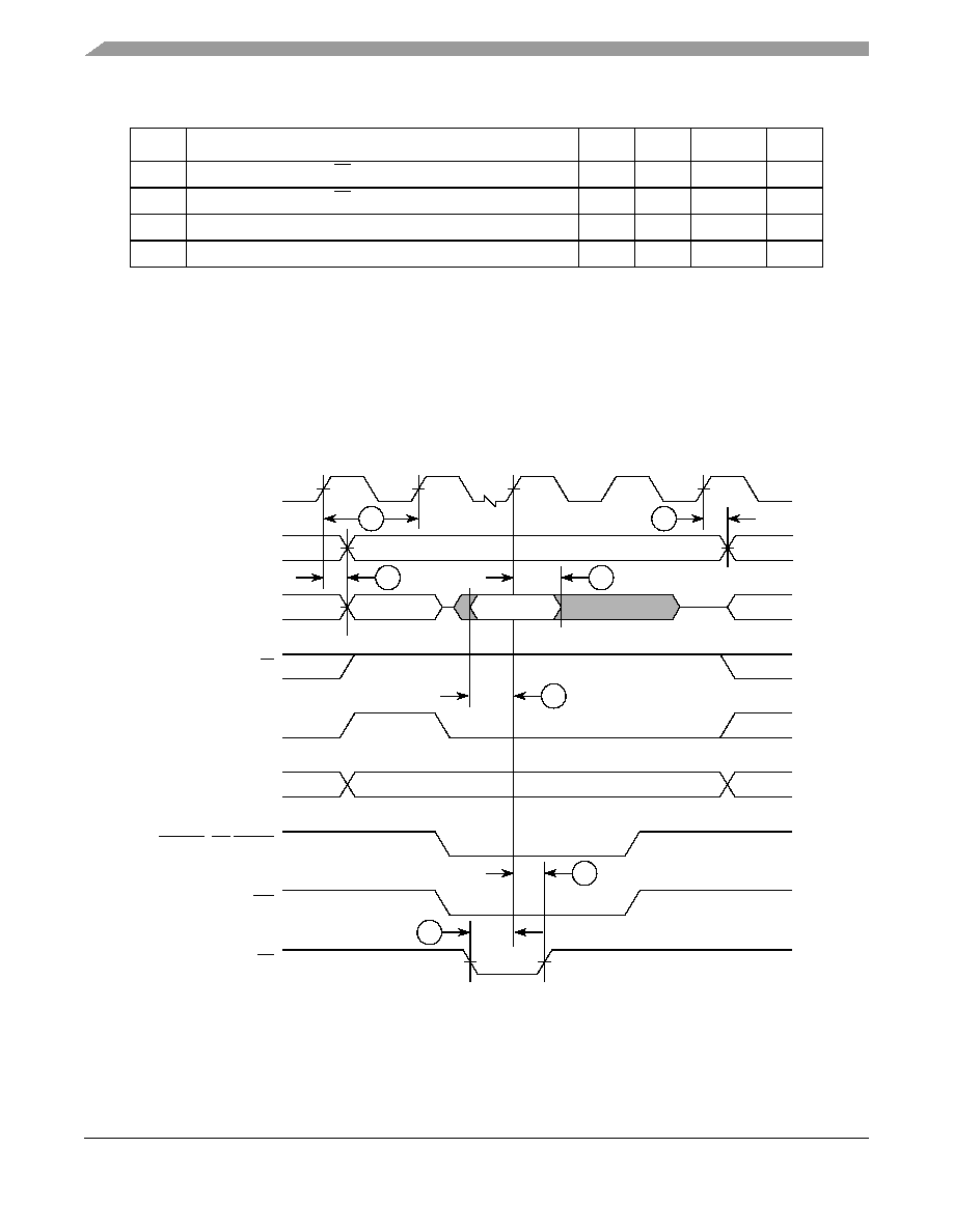
Figure 8. FlexBus Write Timing
9
SDRAM Bus
The SDRAM controller supports accesses to main SDRAM memory from any internal master. It supports
either standard SDRAM or double data rate (DDR) SDRAM, but it does not support both at the same time.
The SDRAM controller uses SSTL2 and SSTL3 I/O drivers. Both SSTL drive modes are programmable
for either Class I or Class II drive strength.
9.1
SDR SDRAM AC Timing Characteristics
The following timing numbers indicate when data will be latched or driven onto the external bus, relative
to the memory bus clock, when operating in SDR mode on write cycles and relative to SDR_DQS on read
cycles. The MCF548x SDRAM controller is a DDR controller that has an SDR mode. Because it is
designed to support DDR, a DQS pulse must still be supplied to the MCF548x for each data beat of an
SDR read. The MCF548x accomplishes this by asserting a signal called SDR_DQS during read cycles.
Care must be taken during board design to adhere to the following guidelines and specs with regard to the
SDR_DQS signal and its usage.
CLKIN
AD[X:0]
AD[31:Y]
R/W
ALE
TSIZ[1:0]
FBCSn, BE/BWEn
TA
FB1
A[X:0]
A[31:Y]
DATA
FB2
FB3
TSIZ[1:0]
FB3
FB6
FB7
OE

MCF548x Integrated Microprocessor Electrical Characteristics, Rev. 2.1
SDRAM Bus
Freescale Semiconductor
12
Table 11. SDR Timing Specifications
Symbol
Characteristic
Min
Max
Unit
Notes
Frequency of Operation
50
133
Mhz
1
NOTES:
1
The frequency of operation is either 2x or 4x the CLKIN frequency of operation. The MCF548X supports a single external
reference clock (CLKIN). This signal defines the frequency of operation for both FlexBus and PCI, but SDRAM clock
operates at the same frequency as the internal bus clock. Please see the PLL chapter of the MCF548X Specification for
more information on setting the SDRAM clock rate.
SD1
Clock Period (t
CK
)
7.52
12
ns
2
2
SDCLK is one SDRAM clock in (ns).
SD2
Clock Skew (t
SK
)
TBD
SD3
Pulse Width High (t
CKH
)
0.45
0.55
SDCLK
3
3
Pulse width high plus pulse width low cannot exceed min and max clock period.
SD4
Pulse Width Low (t
CKL
)
0.45
0.55
SDCLK
4
4
Pulse width high plus pulse width low cannot exceed min and max clock period.
SD5
Address, CKE, CAS, RAS, WE, BA, CS - Output Valid (t
CMV
)
0.5
◊ SDCLK +
1.0ns
ns
SD6
Address, CKE, CAS, RAS, WE, BA, CS - Output Hold (t
CMH
)
2.0
ns
SD7
SDRDQS Output Valid (t
DQSOV
)
Self timed
ns
5
5
SDR_DQS is designed to pulse 0.25 clock before the rising edge of the memory clock. This is a guideline only. Subtle
variation from this guideline is expected. SDR_DQS will only pulse during a read cycle and one pulse will occur for each
data beat.
SD8
SDDQS[3:0] input setup relative to SDCLK (t
DQSIS
)
0.25
◊ SDCLK 0.40 ◊ SDCLK
ns
6
6
SDR_DQS is designed to pulse 0.25 clock before the rising edge of the memory clock. This spec is a guideline only. Subtle
variation from this guideline is expected. SDR_DQS will only pulse during a read cycle and one pulse will occur for each
data beat.
SD9
SDDQS[3:0] input hold relative to SDCLK (t
DQSIH
)
Does not apply. 0.5 SDCLK fixed width.
7
7
The SDR_DQS pulse is designed to be 0.5 clock in width. The timing of the rising edge is most important. The falling edge
does not affect the memory controller.
SD10
Data Input Setup relative to SDCLK (reference only) (t
DIS
)
0.25
◊ SDCLK
ns
8
8
Since a read cycle in SDR mode still uses the DQS circuit within the MCF548X, it is most critical that the data valid window
be centered 1/4 clk after the rising edge of DQS. Ensuring that this happens will result in successful SDR reads. The input
setup spec is just provided as guidance.
SD11
Data Input Hold relative to SDCLK (reference only) (t
DIH
)
1.0
ns
SD12
Data and Data Mask Output Valid (t
DV
)
0.75
◊ SDCLK
+0.500ns
ns
SD13
Data and Data Mask Output Hold (t
DH
)
1.5
ns

SDRAM Bus
MCF548x Integrated Microprocessor Electrical Characteristics, Rev. 2.1
Freescale Semiconductor
13
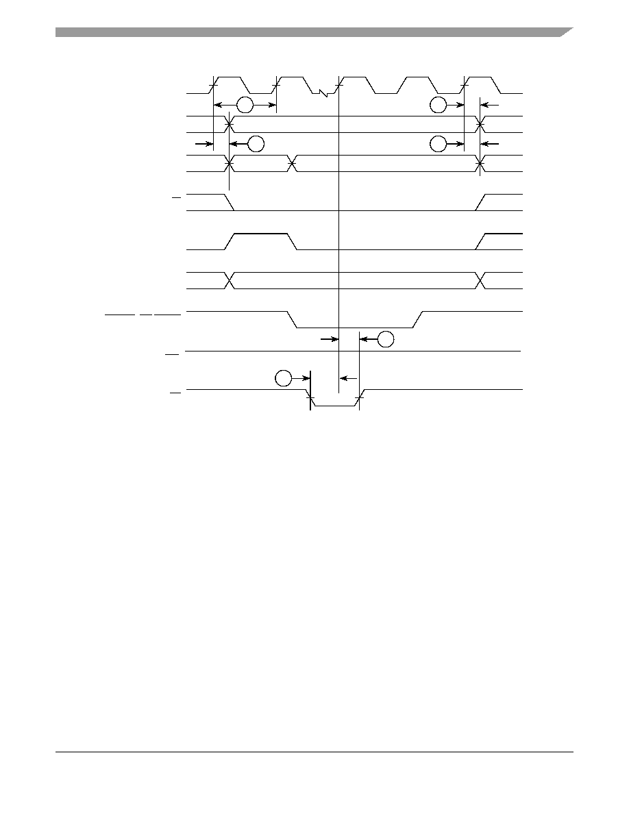
Figure 9. SDR Write Timing
SDCLK0
SDCLK1
SDDM
SDDATA
SDADDR,
SDBA[1:0]
SD2
CMD
ROW
SD2
SD1
SD5
COL
SD6
WD1
WD2
WD3
WD4
SD13
SD12
SD3
SD4
SDCSn,SDWE,
RAS, CAS
MCF548x Integrated Microprocessor Electrical Characteristics, Rev. 2.1
SDRAM Bus
Freescale Semiconductor
14
Figure 10. SDR Read Timing
9.2
DDR SDRAM AC Timing Characteristics
When using the DDR SDRAM controller, the following timing numbers must be followed to properly
latch or drive data onto the memory bus. All timing numbers are relative to the four DQS byte lanes.
Table 12
shows the DDR clock crossover specifications.
Table 12. DDR Clock Crossover Specifications
Symbol
Characteristic
Min
Max
Unit
V
MP
Clock output mid-point voltage
1.05
1.45
V
V
OUT
Clock output voltage level
≠0.3
SD_VDD + 0.3
V
V
ID
Clock output differential voltage (peak to peak swing)
0.7
SD_VDD + 0.6
V
V
IX
Clock crossing point voltage
1
NOTES:
1
The clock crossover voltage is only guaranteed when using the highest drive strength option for the
SDCLK[1:0] and SDCLK[1:0] signals.
1.05 1.45
V
SDCLK0
SDCLK1
SDCSn,SDWE,
SDDM
SDDATA
SDADDR,
RAS, CAS
SDBA[1:0]
SD2
CMD
ROW
SD2
SD1
SD5
COL
WD1
WD2
WD3
WD4
SD10
3/4 MCLK
SDRQS
SDDQS
Delayed
SD11
SD8
Board Delay
SD9
Board Delay
SD7
tDQS
Reference
SDCLK
form
Memories
(Measured at Output Pin)
(Measured at Input Pin)
SD6
NOTE: Data driven from memories relative
to delayed memory clock.
SDRAM Bus
MCF548x Integrated Microprocessor Electrical Characteristics, Rev. 2.1
Freescale Semiconductor
15
Figure 11. DDR Clock Timing Diagram
Table 13. DDR Timing Specifications
Symbol
Characteristic
Min
Max
Unit
Notes
Frequency of Operation
50
1
NOTES:
1
Note that DDR memories typically have a minimum speed specification of 83 MHz. Some vendors go to 75 MHz. Check
with memory component specifications to verify.
133
MHz
2
2
The frequency of operation is either 2x or 4x the CLKIN frequency of operation. The MCF548X supports a single external
reference clock (CLKIN). This signal defines the frequency of operation for both FlexBus and PCI, but SDRAM clock
operates at the same frequency as the internal bus clock. Please see Section 2.2.6, "Reset Configuration Pins."
DD1
Clock Period (t
CK
)
7.52
12
ns
3
3
SDCLK is one memory clock in (ns).
DD2
Pulse Width High (t
CKH
)
0.45
0.55
SDCLK
4
4
Pulse width high plus pulse width low cannot exceed max clock period.
DD3
Pulse Width Low (t
CKL
)
0.45
0.55
SDCLK
5
5
Pulse width high plus pulse width low cannot exceed max clock period.
DD4
Address, SDCKE, CAS, RAS, WE, SDBA, SDCS--Output
Valid (t
CMV
)
--
0.5
◊ SDCLK
+ 1.0 ns
ns
6
6
Command output valid should be 1/2 the memory bus clock (SDCLK) plus some minor adjustments for process,
temperature, and voltage variations.
DD5
Address, SDCKE, CAS, RAS, WE, SDBA, SDCS--Output Hold
(t
CMH
)
2.0
--
ns
DD6
Write Command to first DQS Latching Transition (t
DQSS
)
--
1.25
SDCLK
DD7
Data and Data Mask Output Setup (DQ
->DQS) Relative to
DQS (DDR Write Mode) (t
QS
)
1.0
--
ns
7
8
7
This specification relates to the required input setup time of today's DDR memories. SDDATA[31:24] is relative to
SDDQS3, SDDATA[23:16] is relative to SDDQS2, SDDATA[15:8] is relative to SDDQS1, and SDDATA[7:0] is relative
SDDQS0.
DD8
Data and Data Mask Output Hold (DQS
->DQ) Relative to DQS
(DDR Write Mode) (t
QH
)
1.0
--
ns
9
DD9
Input Data Skew Relative to DQS (Input Setup) (t
IS
)
1
ns
10
DD10
Input Data Hold Relative to DQS (t
IH
)
0.25
◊ SDCLK
+ 0.5ns
--
ns
11
DD11
DQS falling edge to SDCLK rising (output setup time) (t
DSS
)
0.5
--
ns
DD12
DQS falling edge from SDCLK rising (output hold time) (t
DSH
)
0.5
--
ns
DD13
DQS input read preamble width (t
RPRE
)
0.9
1.1
SDCLK
DD14
DQS input read postamble width (t
RPST
)
0.4
0.6
SDCLK
DD15
DQS output write preamble width (t
WPRE
)
0.25
--
SDCLK
DD16
DQS output write postamble width (t
WPST
)
0.4
0.6
SDCLK
SDCLK
SDCLK
V
IX
V
MP
V
IX
V
ID

MCF548x Integrated Microprocessor Electrical Characteristics, Rev. 2.1
SDRAM Bus
Freescale Semiconductor
16
Figure 12. DDR Write Timing
8
The first data beat will be valid before the first rising edge of SDDQS and after the SDDQS write preamble. The remaining
data beats will be valid for each subsequent SDDQS edge.
9
This specification relates to the required hold time of today's DDR memories. SDDATA[31:24] is relative to SDDQS3,
SDDATA[23:16] is relative to SDDQS2, SDDATA[15:8] is relative to SDDQS1, and SDDATA[7:0] is relative SDDQS0.
10
Data input skew is derived from each SDDQS clock edge. It begins with a SDDQS transition and ends when the last data
line becomes valid. This input skew must include DDR memory output skew and system level board skew (due to routing
or other factors).
11
Data input hold is derived from each SDDQS clock edge. It begins with a SDDQS transition and ends when the first data
line becomes invalid.
SDCLK0
SDCLK1
SDCSn,SDWE,
SDDM
SDDATA
SDADDR,
RAS, CAS
SDBA[1:0]
CMD
ROW
DD1
DD5
DD4
COL
WD1 WD2 WD3 WD4
DD7
SDDQS
DD8
DD8
DD7
SDCLK0
SDCLK1
DD3
DD2
DD6

PCI Bus
MCF548x Integrated Microprocessor Electrical Characteristics, Rev. 2.1
Freescale Semiconductor
17
Figure 13. DDR Read Timing
10
PCI Bus
The PCI bus on the MCF548x is PCI 2.2 compliant. The following timing numbers are mostly from the
PCI 2.2 spec. Please refer to the PCI 2.2 spec for a more detailed timing analysis.
Table 14. PCI Timing Specifications
Num
Characteristic
Min
Max
Unit
Notes
Frequency of Operation
25
66
MHz
1
P1
Clock Period (t
CK
)
15.15
33.33
ns
2
P2
Address, Data, and Command (33
< PCI 66 Mhz)--Input Setup (t
IS
)
3.0
--
ns
P3
Address, Data, and Command (0
< PCI 33 Mhz)--Input Setup (t
IS
)
7.0
--
ns
P4
Address, Data, and Command (33-66 Mhz) - Output Valid (t
DV
)
--
6.0
ns
3
P5
Address, Data, and Command (0 -33 Mhz) - Output Valid (t
DV
)
--
11.0
ns
SDCLK0
SDCLK1
SDCSn,SDWE,
SDDQS
SDDATA
SDADDR,
RAS, CAS
SDBA[1:0]
CMD
ROW
DD1
DD5
DD4
WD1 WD2 WD3 WD4
SDDQS
DD9
SDCLK0
SDCLK1
DD3
DD2
SDDATA
WD1 WD2 WD3 WD4
DD10
CL=2
CL=2.5
COL
DQS Read
Preamble
DQS Read
Postamble
DQS Read
Preamble
DQS Read
Postamble

MCF548x Integrated Microprocessor Electrical Characteristics, Rev. 2.1
Fast Ethernet AC Timing Specifications
Freescale Semiconductor
18
Figure 14. PCI Timing
11
Fast Ethernet AC Timing Specifications
11.1 MII/7-WIRE Interface Timing Specs
The following timing specs are defined at the chip I/O pin and must be translated appropriately to arrive
at timing specs/constraints for the EMAC_10_100 I/O signals.
The following timing specs meet the requirements for both MII and 7-Wire style interfaces for a range of
transceiver devices. If this interface is to be used with a specific transceiver device the timing specs may
be altered to match that specific transceiver.
P6
PCI signals (0 - 66 Mhz) - Output Hold (t
DH
)
0
--
ns
4
P7
PCI signals (0 - 66 Mhz) - Input Hold (t
IH
)
0
--
ns
5
P8
PCI REQ/GNT (33
< PCI 66Mhz) - Output valid (t
DV
)
--
6
ns
6
P9
PCI REQ/GNT (0
< PCI 33Mhz) - Output valid (t
DV
)
--
12
ns
P10
PCI REQ/GNT (33
< PCI 66Mhz) - Input Setup (t
IS
)
--
5
ns
P11
PCI REQ (0
< PCI 33Mhz) - Input Setup (t
IS
)
12
--
ns
P12
PCI GNT (0
< PCI 33Mhz) - Input Setup (t
IS
)
10
--
ns
NOTES:
1
Please see Section 2.2.6, "Reset Configuration Pins," for more information on setting the PCI clock rate. Also
specific guidelines may need to be followed when operating the system PLL below certain frequencies.
2
Max cycle rate is determined by CLKIN and how the user has the system PLL configured.
3
All signals defined as PCI bused signals. Does not include PTP (point-to-point) signals.
4
PCI 2.2 spec does not require an output hold time. Although the MCF548X may provide a slight amount of hold, it
is not required or guaranteed.
5
PCI 2.2 spec requires zero input hold.
6
These signals are defined at PTP (Point-to-point) in the PCI 2.2 spec.
Table 14. PCI Timing Specifications (continued)
Num
Characteristic
Min
Max
Unit
Notes
CLKIN
Input
Setup/Hold
P1
P4
P6
P2
P7
Output Valid
Input Valid
Output
Valid/Hold

Fast Ethernet AC Timing Specifications
MCF548x Integrated Microprocessor Electrical Characteristics, Rev. 2.1
Freescale Semiconductor
19
Figure 15. MII Receive Signal Timing Diagram
11.2 MII Transmit Signal Timing
Figure 16. MII Transmit Signal Timing Diagram
Table 15. MII Receive Signal Timing
Num
Characteristic
Min
Max
Unit
M1
RXD[3:0], RXDV, RXER to RXCLK setup
5
--
ns
M2
RXCLK to RXD[3:0], RXDV, RXER hold
5
--
ns
M3
RXCLK pulse width high
35%
65%
RXCLK period
M4
RXCLK pulse width low
35%
65%
RXCLK period
Table 16. MII Transmit Signal Timing
Num
Characteristic
Min
Max
Unit
M5
TXCLK to TXD[3:0], TXEN, TXER invalid
0
--
ns
M6
TXCLK to TXD[3:0], TXEN, TXER valid
--
25
ns
M7
TXCLK pulse width high
35%
65%
TXCLK period
M8
TXCLK pulse width low
35%
65%
TXCLK period
RXCLK (Input)
RXD[3:0] (Inputs)
RXDV,
RXER
M3
M4
M1
M2
TXCLK (Input)
TXD[3:0] (Outputs)
TXEN,
TXER
M7
M8
M5
M6
MCF548x Integrated Microprocessor Electrical Characteristics, Rev. 2.1
Fast Ethernet AC Timing Specifications
Freescale Semiconductor
20
11.3 MII Async Inputs Signal Timing (CRS, COL)
Figure 17. MII Async Inputs Timing Diagram
11.4 MII Serial Management Channel Timing (MDIO,MDC)
Figure 18. MII Serial Management Channel TIming Diagram
Table 17. MII Transmit Signal Timing
Num
Characteristic
Min
Max
Unit
M9
CRS, COL minimum pulse width
1.5
--
TX_CLK period
Table 18. MII Serial Management Channel Signal Timing
Num
Characteristic
Min
Max
Unit
M10
MDC falling edge to MDIO output invalid
(min prop delay)
0
--
ns
M11
MDC falling edge to MDIO output valid
(max prop delay)
--
25
ns
M12
MDIO (input) to MDC rising edge setup
10
--
ns
M13
MDIO (input) to MDC rising edge hold
0
--
ns
M14
MDC pulse width high
40%
60%
MDC period
M15
MDC pulse width low
40%
60%
MDC period
CRS, COL
M9
MDC (Output)
M14
MDIO (Output)
MDIO (Input)
M15
M10
M11
M12
M13
General Timing Specifications
MCF548x Integrated Microprocessor Electrical Characteristics, Rev. 2.1
Freescale Semiconductor
21
12
General Timing Specifications
Table 19
lists timing specifications for the GPIO, PSC, FlexCAN, DREQ, DACK, and external interrupts.
13
I
2
C Input/Output Timing Specifications
Table 20
lists specifications for the I
2
C input timing parameters shown in
Figure 19
.
Table 21
lists specifications for the I
2
C output timing parameters shown in
Figure 19
.
Table 19. General AC Timing Specifications
Name
Characteristic Min
Max
Unit
G1
CLKIN high to signal output valid
--
2
PSTCLK
G2
CLKIN high to signal invalid (output hold)
0
--
ns
G3
Signal input pulse width
2
--
PSTCLK
Table 20. I
2
C Input Timing Specifications between SCL and SDA
Num
Characteristic
Min
Max
Units
I1
Start condition hold time
2
--
Bus clocks
I2
Clock low period
8
--
Bus clocks
I3
SCL/SDA rise time (V
IL
= 0.5 V to V
IH
= 2.4 V)
--
1
mS
I4
Data hold time
0
--
ns
I5
SCL/SDA fall time (V
IH
= 2.4 V to V
IL
= 0.5 V)
--
1
mS
I6
Clock high time
4
--
Bus clocks
I7
Data setup time
0
--
ns
I8
Start condition setup time (for repeated start condition only)
2
--
Bus clocks
I9
Stop condition setup time
2
--
Bus clocks
MCF548x Integrated Microprocessor Electrical Characteristics, Rev. 2.1
I
2
C Input/Output Timing Specifications
Freescale Semiconductor
22
Figure 19
shows timing for the values in
Table 20
and
Table 21
.
Figure 19. I
2
C Input/Output Timings
Table 21. I
2
C Output Timing Specifications between SCL and SDA
Num
Characteristic
Min
Max
Units
I1
1
NOTES:
1
Note: Output numbers depend on the value programmed into the IFDR; an IFDR programmed
with the maximum frequency (IFDR = 0x20) results in minimum output timings as shown in
Table 21
. The I
2
C interface is designed to scale the actual data transition time to move it to the
middle of the SCL low period. The actual position is affected by the prescale and division values
programmed into the IFDR; however, the numbers given in
Table 21
are minimum values.
Start condition hold time
6
--
Bus clocks
I2
1
Clock low period
10
--
Bus clocks
I3
2
2
Because SCL and SDA are open-collector-type outputs, which the processor can only actively
drive low, the time SCL or SDA take to reach a high level depends on external signal
capacitance and pull-up resistor values.
SCL/SDA rise time (V
IL
= 0.5 V to V
IH
= 2.4 V)
--
--
µS
I4
1
Data hold time
7
--
Bus clocks
I5
3
3
Specified at a nominal 50-pF load.
SCL/SDA fall time (V
IH
= 2.4 V to V
IL
= 0.5 V)
--
3
ns
I6
1
Clock high time
10
--
Bus clocks
I7
1
Data setup time
2
--
Bus clocks
I8
1
Start condition setup time (for repeated start
condition only)
20
--
Bus clocks
I9
1
Stop condition setup time
10
--
Bus clocks
SCL
I2
I6
I1
I4
I5
I7
I8
I3
I9
SDA
JTAG and Boundary Scan Timing
MCF548x Integrated Microprocessor Electrical Characteristics, Rev. 2.1
Freescale Semiconductor
23
14
JTAG and Boundary Scan Timing
Figure 20. Test Clock Input Timing
Table 22. JTAG and Boundary Scan Timing
Num
Characteristics
1
NOTES:
1
MTMOD is expected to be a static signal. Hence, it is not associated with any timing
Symbol
Min
Max
Unit
J1
TCLK Frequency of Operation
f
JCYC
DC
10
MHz
J2
TCLK Cycle Period
t
JCYC
2
--
t
CK
J3
TCLK Clock Pulse Width
t
JCW
15.15
--
ns
J4
TCLK Rise and Fall Times
t
JCRF
0.0
3.0
ns
J5
Boundary Scan Input Data Setup Time to TCLK Rise
t
BSDST
5.0
--
ns
J6
Boundary Scan Input Data Hold Time after TCLK Rise
t
BSDHT
24.0
--
ns
J7
TCLK Low to Boundary Scan Output Data Valid
t
BSDV
0.0
15.0
ns
J8
TCLK Low to Boundary Scan Output High Z
t
BSDZ
0.0
15.0
ns
J9
TMS, TDI Input Data Setup Time to TCLK Rise
t
TAPBST
5.0
--
ns
J10
TMS, TDI Input Data Hold Time after TCLK Rise
t
TAPBHT
10.0
--
ns
J11
TCLK Low to TDO Data Valid
t
TDODV
0.0
15.0
ns
J12
TCLK Low to TDO High Z
t
TDODZ
0.0
15.0
ns
J13
TRST Assert Time
t
TRSTAT
100.0
--
ns
J14
TRST Setup Time (Negation) to TCLK High
t
TRSTST
10.0
--
ns
TCLK (Input)
J2
J3
J3
J4
J4
V
IH
V
IL

MCF548x Integrated Microprocessor Electrical Characteristics, Rev. 2.1
JTAG and Boundary Scan Timing
Freescale Semiconductor
24
Figure 21. Boundary Scan (JTAG) Timing
Figure 22. Test Access Port Timing
Figure 23. TRST Timing Debug AC Timing Specifications
Output Data Valid
TCLK
Data Inputs
Data Outputs
Data Outputs
Data Outputs
5
6
Input Data Valid
7
Output Data Valid
8
7
V
IH
V
IL
Output Data Valid
TCLK
TDI, TMS, BKPT
TDO
TDO
TDO
9
10
Input Data Valid
11
Output Data Valid
12
11
V
IH
V
IL
TCLK
TRST
14
13
JTAG and Boundary Scan Timing
MCF548x Integrated Microprocessor Electrical Characteristics, Rev. 2.1
Freescale Semiconductor
25
Table 23
lists specifications for the debug AC timing parameters shown in
Figure 25
.
Figure 24
shows real-time trace timing for the values in
Table 23
.
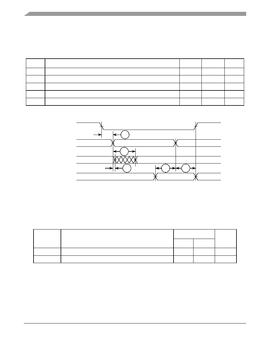
Figure 24. Real-Time Trace AC Timing
Figure 25
shows BDM serial port AC timing for the values in
Table 23
.
Figure 25. BDM Serial Port AC Timing
Table 23. Debug AC Timing Specification
Num
Characteristic
66 MHz
Units
Min
Max
D1
PSTDDATA to PSTCLK setup
4.5
ns
D2
PSTCLK to PSTDDATA hold
4.5
ns
D3
DSI-to-DSCLK setup
1
PSTCLKs
D4
1
NOTES:
1
DSCLK and DSI are synchronized internally. D4 is measured from the
synchronized DSCLK input relative to the rising edge of CLKOUT.
DSCLK-to-DSO hold
4
PSTCLKs
D5
DSCLK cycle time
5
PSTCLKs
PSTCLK
PSTDDATA[7:0]
D1
D2
Past
Current
DSCLK
DSI
DSO
Next
Current
D5
D3
D4
MCF548x Integrated Microprocessor Electrical Characteristics, Rev. 2.1
DSPI Electrical Specifications
Freescale Semiconductor
26
15
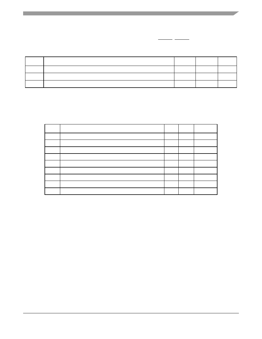
DSPI Electrical Specifications
Table 24
lists DSPI timings.
The values in
Table 24
correspond to
Figure 26
.
Figure 26. DSPI Timing
16
Timer Module AC Timing Specifications
Table 25
lists timer module AC timings.
Table 24. DSPI Modules AC Timing Specifications
Name
Characteristic Min
Max
Unit
DS1
DSPI_CS[3:0] to DSPI_CLK
1
◊ tck
510
◊ tck
ns
DS2
DSPI_CLK high to DSPI_DOUT valid.
--
12
ns
DS3
DSPI_CLK high to DSPI_DOUT invalid. (Output hold)
2
--
ns
DS4
DSPI_DIN to DSPI_CLK (Input setup)
10
--
ns
DS5
DSPI_DIN to DSPI_CLK (Input hold)
10
--
ns
Table 25. Timer Module AC Timing Specifications
Name
Characteristic
0≠66 MHz
Unit
Min
Max
T1
TIN0 / TIN1 / TIN2 / TIN3 cycle time
3
--
PSTCLK
T2
TIN0 / TIN1 / TIN2 / TIN3 pulse width
1
--
PSTCLK
DSPI_CS[3:0]
DSPI_CLK
DSPI_DOUT
DSPI_DIN
DS5
DS4
DS1
DS2
DS3

THIS PAGE INTENTIONALLY LEFT BLANK
MCF548x Integrated Microprocessor Electrical Characteristics, Rev. 2.1
Freescale Semiconductor
27

How to Reach Us:
Home Page:
www.freescale.com
E-mail:
support@freescale.com
USA/Europe or Locations Not Listed:
Freescale Semiconductor
Technical Information Center, CH370
1300 N. Alma School Road
Chandler, Arizona 85224
+1-800-521-6274 or +1-480-768-2130
support@freescale.com
Europe, Middle East, and Africa:
Freescale Halbleiter Deutschland GmbH
Technical Information Center
Schatzbogen 7
81829 Muenchen, Germany
+44 1296 380 456 (English)
+46 8 52200080 (English)
+49 89 92103 559 (German)
+33 1 69 35 48 48 (French)
support@freescale.com
Japan:
Freescale Semiconductor Japan Ltd.
Technical Information Center
3-20-1, Minami-Azabu, Minato-ku
Tokyo 106-0047, Japan
0120 191014 or +81 3 3440 3569
support.japan@freescale.com
Asia/Pacific:
Freescale Semiconductor Hong Kong Ltd.
Technical Information Center
2 Dai King Street
Tai Po Industrial Estate
Tai Po, N.T., Hong Kong
+800 2666 8080
support.asia@freescale.com
For Literature Requests Only:
Freescale Semiconductor Literature Distribution Center
P.O. Box 5405
Denver, Colorado 80217
1-800-441-2447 or 303-675-2140
Fax: 303-675-2150
LDCForFreescaleSemiconductor@hibbertgroup.com
Information in this document is provided solely to enable system and
software implementers to use Freescale Semiconductor products. There are
no express or implied copyright licenses granted hereunder to design or
fabricate any integrated circuits or integrated circuits based on the
information in this document.
Freescale Semiconductor reserves the right to make changes without further
notice to any products herein. Freescale Semiconductor makes no warranty,
representation or guarantee regarding the suitability of its products for any
particular purpose, nor does Freescale Semiconductor assume any liability
arising out of the application or use of any product or circuit, and specifically
disclaims any and all liability, including without limitation consequential or
incidental damages. "Typical" parameters that may be provided in Freescale
Semiconductor data sheets and/or specifications can and do vary in different
applications and actual performance may vary over time. All operating
parameters, including "Typicals", must be validated for each customer
application by customer's technical experts. Freescale Semiconductor does
not convey any license under its patent rights nor the rights of others.
Freescale Semiconductor products are not designed, intended, or authorized
for use as components in systems intended for surgical implant into the body,
or other applications intended to support or sustain life, or for any other
application in which the failure of the Freescale Semiconductor product could
create a situation where personal injury or death may occur. Should Buyer
purchase or use Freescale Semiconductor products for any such unintended
or unauthorized application, Buyer shall indemnify and hold Freescale
Semiconductor and its officers, employees, subsidiaries, affiliates, and
distributors harmless against all claims, costs, damages, and expenses, and
reasonable attorney fees arising out of, directly or indirectly, any claim of
personal injury or death associated with such unintended or unauthorized
use, even if such claim alleges that Freescale Semiconductor was negligent
regarding the design or manufacture of the part.
FreescaleTM and the Freescale logo are trademarks of Freescale
Semiconductor, Inc. All other product or service names are the property
of their respective owners.© Freescale Semiconductor, Inc. 2004. All rights
reserved.
MCF5485EC
Rev. 2.1
12/2004