 | –≠–ª–µ–∫—Ç—Ä–æ–Ω–Ω—ã–π –∫–æ–º–ø–æ–Ω–µ–Ω—Ç: MCIMX31 | –°–∫–∞—á–∞—Ç—å:  PDF PDF  ZIP ZIP |
© Freescale Semiconductor, Inc., 2005, 2006. All rights reserved.
Preliminary
Freescale Semiconductor
Advance Information
This document contains information on a new product. Specifications and information herein are subject to change without notice.
Document Number: MCIMX31
Rev. 1.4, 04/2006
MCIMX31 and
MCIMX31L
Package Information
Plastic Package
Case 1581-01 14 x 14 mm, 0.5 P
Ordering Information
Device
Operating
Temperature Range
Package
MCIMX31VKN5
0
∞C to +70∞C
MAPBGA≠457
MCIMX31LVKN5
0
∞C to +70∞C
MAPBGA≠457
1
Introduction
The i.MX31 (MCIMX31) and i.MX31L (MCIMX31L)
are multimedia applications processors that represent the
next step in low-power, high-performance application
processors. Unless otherwise specified, the material in
this data sheet is applicable to both the i.MX31 and
i.MX31L processors.
Based on an ARM11
TM
microprocessor core, the
i.MX31 and i.MX31L provide the performance with
low power consumption required by modern digital
devices such as:
∑
Feature-rich cellular phones
∑
Portable media players and mobile gaming
machines
∑
Personal digital assistants (PDAs) and Wireless
PDAs
∑
Portable DVD players
∑
Digital cameras
The i.MX31 and i.MX31L take advantage of the
ARM1136JF-S
TM
core running at typical speeds of
532 MHz, and is optimized for minimal power
i.MX31 and i.MX31L
Multimedia Applications
Processors
Contents
1 Introduction . . . . . . . . . . . . . . . . . . . . . . . . . . 1
1.1 Features . . . . . . . . . . . . . . . . . . . . . . . . . . . 2
1.2 Block Diagram . . . . . . . . . . . . . . . . . . . . . . 2
2 Functional Description and Application
Information . . . . . . . . . . . . . . . . . . . . . . . . . . . 3
2.1 ARM11 Microprocessor Core . . . . . . . . . . . 3
2.2 Module Inventory . . . . . . . . . . . . . . . . . . . . 5
2.3 Module Descriptions . . . . . . . . . . . . . . . . . . 8
3 Signal Descriptions . . . . . . . . . . . . . . . . . . . 23
3.1 i.MX31 and i.MX31L I/O Pad Signal
Settings . . . . . . . . . . . . . . . . . . . . . . . . . . 23
4 Electrical Characteristics . . . . . . . . . . . . . . 60
4.1 i.MX31 and i.MX31L
Chip-Level Conditions . . . . . . . . . . . . . . . 60
4.2 Supply Power-Up Requirements and
Restrictions . . . . . . . . . . . . . . . . . . . . . . . 65
4.3 Module-Level Electrical Specifications . . . 66
5 Package Information and Pinout . . . . . . . 152
5.1 MAPBGA Production Package
457 14 x 14 mm, 0.5 P . . . . . . . . . . . . . . 153
6 Product Documentation . . . . . . . . . . . . . . . 167
6.1 Revision History . . . . . . . . . . . . . . . . . . . 167

i.MX31/i.MX31L Advance Information, Rev. 1.4
2
Freescale Semiconductor
Preliminary
Introduction
consumption using the most advanced techniques for power saving (DPTC, DVFS, power gating, clock
gating). With 90 nm technology and dual-Vt transistors (two threshold voltages), the i.MX31 and
i.MX31L provide the optimal performance versus leakage current balance.
The performance of the i.MX31 and i.MX31L is boosted by a multi-level cache system, and features
peripheral devices such as an MPEG-4 Hardware Encoder (VGA, 30 fps), an Autonomous Image
Processing Unit, a Vector Floating Point (VFP11) co-processor, and a RISC-based SDMA controller.
The i.MX31 and i.MX31L support connections to various types of external memories, such as 266 MHz
DDR, NAND Flash, NOR Flash, SDRAM, and SRAM. The i.MX31 and i.MX31L can be connected to a
variety of external devices using technology, such as high-speed USB2.0 OTG, ATA, MMC/SDIO, and
compact flash.
1.1
Features
The i.MX31 and i.MX31L are designed for the high-tier and mid-tier smartphone markets. They provide
low-power solutions for high-performance demanding multimedia and graphics applications.
The i.MX31 and i.MX31L are built around the ARM11 MCU core and implemented in the 90 nm
technology.
The systems include the following features:
∑
Multimedia and floating-point hardware acceleration supporting:
-- MPEG-4 real-time encode of up to VGA at 30 fps
-- MPEG-4 real-time video post-processing of up to VGA at 30 fps
-- Video conference call of up to QCIF-30 fps (decoder in software), 128 kbps
-- Video streaming (playback) of up to VGA-30 fps, 384 kbps
-- 3D graphics and other applications acceleration with the ARM
Æ
tightly-coupled Vector
Floating Point co-processor
-- On-the-fly video processing that reduces system memory load (for example, the
power-efficient viewfinder application with no involvement of either the memory system or the
ARM CPU)
∑
Advanced power management
-- Dynamic voltage and frequency scaling
-- Multiple clock and power domains
-- Independent gating of power domains
∑
Multiple communication and expansion ports including a fast parallel interface to an external
graphic accelerator (supporting major graphic accelerator vendors)
1.2
Block Diagram
Figure 1
shows the i.MX31 and i.MX31L simplified interface block diagram.
Functional Description and Application Information
i.MX31/i.MX31L Advance Information, Rev. 1.4
Freescale Semiconductor
3
Preliminary
Figure 1. i.MX31/i.MX31L Simplified Interface Block Diagram
Table 1
provides additional details on the i.MX31 and i.MX31L orderable parts.
2
Functional Description and Application Information
2.1
ARM11 Microprocessor Core
The CPU of the i.MX31 and i.MX31L is the ARM1136JF-S core based on the ARM v6 architecture. It
supports the ARM Thumb
Æ
instruction sets, features Jazelle
Æ
technology (which enables direct execution
of Java byte codes), and a range of SIMD DSP instructions that operate on 16-bit or 8-bit data values in
32-bit registers.
Table 1. Orderable Part Details
Device
Operating Temp.
Range (T
A
)
Package
RoHS
Compliant
Pb-Free
MSL
Level
Solder
Temp.
MCIMX31VKN5
≠0∞C to +70∞C
457-lead MAPBGA
0.5 mm, 14 mm x 14 mm
Yes
Yes
3
260
∞C
MCIMX31LVKN5
≠0∞C to +70∞C
457-lead MAPBGA
0.5 mm, 14 mm x 14 mm
Yes
Yes
3
260
∞C
External Memory
AP Peripherals
SRAM, PSRAM,
SDRAM
NAND Flash,
SmartMedia
GPU*
Camera
MPEG-4
Baseband
SD
Card
Fast
IrDA
USB
Image Processing Unit (IPU)
Parallel
Sensor (2)
Serial
LCD
Timers
AUDMUX
SSI (2)
UART (5)
GPT
PWM
EPIT (2)
RTC
GPIO
WDOG
1-WIRE
Æ
CSPI (3)
I2C (3)
FIR
KPP
CCM
ARM11
TM
Platform
I-Cache
D-Cache
L2-Cache
ROMPATCH
VFP
SDMA
USB-OTG
IIM
Expansion
SIM
ATA
PCMCIA/CF
Mem Stick (2)
SDHC (2)
USB Host (2)
* GPU unavailable for i.MX31L
Inversion and Rotation
Camera Interface
Blending
Display/TV Ctl
Pre & Post Processing
Display (2)
NOR Flash
DDR
WLAN
Bluetooth
Interface (EMI)
Power
Management
IC
PC
Card
PC
Card
Host/Device
Mouse
Keyboard
Tamper
Detection
Serial
EPROM
Video Encoder
8 x 8
Keypad
GPS
ATA
Hard Drive
ARM1136JF-S
TM
MAX
Memory
Internal
Security
RNGA
SCC
RTIC
Debug
ECT
SJC
ETM

i.MX31/i.MX31L Advance Information, Rev. 1.4
4
Freescale Semiconductor
Preliminary
Functional Description and Application Information
The ARM1136JF-S processor core features:
∑
Integer unit with integral EmbeddedICE
TM
logic
∑
Eight-stage pipeline
∑
Branch prediction with return stack
∑
Low-interrupt latency
∑
Instruction and data memory management units (MMUs), managed using micro TLB structures
backed by a unified main TLB
∑
Instruction and data L1 caches, including a non-blocking data cache with Hit-Under-Miss
∑
Virtually indexed/physically addressed L1 caches
∑
64-bit interface to both L1 caches
∑
Write buffer (bypassable)
∑
High-speed Advanced Micro Bus Architecture (AMBA)
TM
L2 interface
∑
Vector Floating Point co-processor (VFP) for 3D graphics and other floating-point applications
hardware acceleration
∑
ETM
TM
and JTAG-based debug support
2.1.1
Performance
ARM1136JF-S operating frequency in C90LP process:
∑
532 MHz (4
◊ 133 MHz) (wcs)
2.1.2
Memory System
The ARM1136JF-S complex includes 16 KB Instruction and 16 KB Data L1 caches. It connects to the
i.MX31 and i.MX31L L2 unified cache through 64-bit instruction (read-only), 64-bit data read/write
(bi-directional), and 64-bit data write interfaces.
The embedded 16K SRAM can be used for audio streaming data to avoid external memory accesses for
the Low Power Audio Playback, for Security, or for other applications. There is also a 32-KB ROM for
bootstrap code and other frequently-used code and data.
A ROM patch module provides the ability to patch the internal ROM. It can also initiate an external boot
by overriding the boot reset sequence by a jump to a configurable address.
Table 2
shows information about the i.MX31 and i.MX31L core in tabular form.
Functional Description and Application Information
i.MX31/i.MX31L Advance Information, Rev. 1.4
Freescale Semiconductor
5
Preliminary
2.2
Module Inventory
Table 3
shows an alphabetical listing of the modules in the multimedia applications processor. A
cross-reference is provided directly to each module description for more information.
Table 2. i.MX31/i.MX31L Core
Core
Acronym
Core
Name
Brief Description
Integrated Memory
Includes
ARM11 or
ARM1136
ARM1136
Platform
The ARM1136TM Platform consists of the ARM1136JF-S core, the ETM
real-time debug modules, a 6 x 5 multi-layer AHB crossbar switch (MAX), and a
Vector Floating Processor (VFP).
The i.MX31/i.MX31L provide a high-performance ARM11 microprocessor core
and highly integrated system functions. The ARM Application Processor (AP)
and other subsystems address the needs of the personal, wireless, and portable
product market with integrated peripherals, advanced processor core, and
power management capabilities.
∑ 16 Kbyte
Instruction Cache
∑ 16 Kbyte Data
Cache
∑ 128 Kbyte L2
Cache
∑ 32 Kbyte ROM
∑ 16 Kbyte RAM
Table 3. Digital and Analog Modules
Block
Mnemonic
Block Name
Functional
Grouping
Brief Description3
Section/
Page
1-WireÆ
1-Wire Interface Connectivity
Peripheral
The 1-Wire module provides bi-directional communication between
the ARM11 core and the Add-Only-Memory EPROM (DS2502).
The 1-Kbit EPROM is used to hold information about battery and
communicates with the ARM11 platform using the IP interface.
2.3.1/8
ATA
Advanced
Technology (AT)
Attachment
Connectivity
Peripheral
The ATA block is an AT attachment host interface. It is designed to
interface with IDE hard disc drives and ATAPI optical disc drives.
2.3.2/8
AUDMUX
Digital Audio
Multiplexer
Multimedia
Peripheral
The AUDMUX interconnections allow multiple, simultaneous
audio/voice/data flows between the ports in point-to-point or
point-to-multipoint configurations.
2.3.3/9
CCM
Clock Control
Module
Clock
The CCM provides clock, reset, and power management control for
the i.MX31 and i.MX31L.
2.3.4/9
CSPI
Configurable
Serial Peripheral
Interface (x 3)
Connectivity
Peripheral
The CSPI is equipped with data FIFOs and is a master/slave
configurable serial peripheral interface module, capable of
interfacing to both SPI master and slave devices.
2.3.5/10
ECT
Embedded
Cross Trigger
Debug
The ECT is composed of three CTIs (Cross Trigger Interface) and
one CTM (Cross Trigger Matrix--key in the multi-core and multi-IP
debug strategy.
2.3.6/10
EMI
External
Memory
Interface
Memory
Interface (EMI)
The EMI includes
∑ Multi-Master Memory Interface (M3IF)
∑ Enhanced SDRAM/MDDR memory controller (SDRAMC)
∑ NAND Flash Controller (NFC)
∑ Wireless External Interface Module (WEIM)
2.3.7/11
EPIT
Enhanced
Periodic
Interrupt Timer
Timer
Peripheral
The EPIT is a 32-bit "set and forget" timer which starts counting
after the EPIT is enabled by software. It is capable of providing
precise interrupts at regular intervals with minimal processor
intervention.
2.3.8/12

i.MX31/i.MX31L Advance Information, Rev. 1.4
6
Freescale Semiconductor
Preliminary
Functional Description and Application Information
FIR
Fast InfraRed
Interface
Connectivity
Peripheral
This FIR is capable of establishing a 0.576 Mbit/s, 1.152 Mbit/s or 4
Mbit/s half duplex link via a LED and IR detector. It supports 0.576
Mbit/s, 1.152 Mbit/s medium infrared (MIR) physical layer protocol
and 4Mbit/s fast infrared (FIR) physical layer protocol defined by
IrDA, version 1.4.
2.3.9/12
GPIO
General
Purpose I/O
Module
Pins
The GPIO provides 32 bits of bidirectional, general purpose I/O.
This peripheral provides dedicated general-purpose pins that can
be configured as either inputs or outputs.
2.3.10/12
GPT
General
Purpose Timer
Timer
Peripheral
The GPT is a multipurpose module used to measure intervals or
generate periodic output.
2.3.11/12
GPU
Graphics
Processing Unit
Multimedia
Peripheral
The GPU provides hardware acceleration for 2D and 3D graphics
algorithms.
2.3.12/13
I2C
Inter IC
Communication
Connectivity
Peripheral
The I2C provides serial interface for controlling the Sensor Interface
and other external devices. Data rates of up to 100 Kbits/s are
supported.
2.3.13/13
IIM
IC Identification
Module
Security
The IIM provides an interface for reading--and in some cases,
programming, and overriding identification and control information
stored in on-chip fuse elements.
2.3.14/13
IPU
Image
Processing Unit
Multimedia
Peripheral
The IPU supports video and graphics processing functions in the
i.MX31 and i.MX31L and interfaces to video, still image sensors,
and displays.
2.3.15/14
KPP
Keypad Port
Connectivity
Peripheral
The KPP is used for key pad matrix scanning or as a general
purpose I/O. This peripheral simplifies the software task of scanning
a keypad matrix.
2.3.16/15
MPEG-4
MPEG-4 Video
Encoder
Multimedia
Peripherals
The MPEG-4 encoder accelerates video compression, following the
MPEG-4 standard
2.3.17/15
PCMCIA
PCM
Connectivity
Peripheral
The PCMCIA Host Adapter provides the control logic for PCMCIA
socket interfaces.
2.3.19/16
PWM
Pulse-Width
Modulator
Timer
Peripheral
The PWM has a 16-bit counter and is optimized to generate sound
from stored sample audio images. It can also generate tones.
2.3.20/16
RNGA
Random
Number
Generator
Accelerator
Security
The RNGA module is a digital integrated circuit capable of
generating 32-bit random numbers. It is designed to comply with
FIPS-140 standards for randomness and non-determinism.
2.3.21/16
RTC
Real Time Clock Timer
Peripheral
The RTC module provides a current stamp of seconds, minutes,
hours, and days. Alarm and timer functions are also available for
programming. The RTC support dates from the year 1980 to 2050.
2.3.22/16
RTIC
Run-Time
Integrity
Checkers
Security
The RTIC ensures the integrity of the peripheral memory contents
and assists with boot authentication.
2.3.23/17
Table 3. Digital and Analog Modules (continued)
Block
Mnemonic
Block Name
Functional
Grouping
Brief Description3
Section/
Page

Functional Description and Application Information
i.MX31/i.MX31L Advance Information, Rev. 1.4
Freescale Semiconductor
7
Preliminary
SCC
Security
Controller
Module
Security
The SCC is a hardware component composed of two blocks--the
Secure RAM module, and the Security Monitor. The Secure RAM
provides a way of securely storing sensitive information. The
Security Monitor implements the security policy, checking algorithm
sequencing, and controlling the Secure State.
2.3.24/17
SDHC
Secured Digital
Host Controller
Connectivity
Peripheral
The SDHC controls the MMC (MultiMediaCard), SD (Secure
Digital) memory, and I/O cards by sending commands to cards and
performing data accesses to and from the cards.
2.3.25/18
SDMA
SDMA
System
Control
Peripheral
The SDMA controller maximizes the system's performance by
relieving the ARM core of the task of bulk data transfer from memory
to memory or between memory and on-chip peripherals.
2.3.26/18
SIM
Subscriber
Identification
Module
Connectivity
Peripheral
The SIM interfaces to an external Subscriber Identification Card. It
is an asynchronous serial interface adapted for Smart Card
communication for e-commerce applications.
2.3.27/20
SJC
Secure JTAG
Controller
Debug
The SJC provides debug and test control with maximum security
and provides a flexible architecture for future derivatives or future
multi-cores architecture.
2.3.28/20
SSI
Synchronous
Serial Interface
Multimedia
Peripheral
The SSI is a full-duplex, serial port that allows the chip to
communicate with a variety of serial devices, such as standard
codecs, Digital Signal Processors (DSPs), microprocessors,
peripherals, and popular industry audio codecs that implement the
inter-IC sound bus standard (I2S) and Intel AC97 standard.
2.3.29/20
UART
Universal
Asynchronous
Receiver/Trans
mitter
Connectivity
Peripheral
The UART provides serial communication capability with external
devices through an RS-232 cable or through use of external
circuitry that converts infrared signals to electrical signals (for
reception) or transforms electrical signals to signals that drive an
infrared LED (for transmission) to provide low speed IrDA
compatibility.
2.3.30/21
USB
Universal Serial
Bus--
2 Host
Controllers and
1 OTG
(On-The-Go)
Connectivity
Peripherals
∑ USB Host 1 is designed to support transceiverless connection to
the on-board peripherals in Low Speed and Full Speed mode,
and connection to the ULPI (UTMI+ Low-Pin Count) and Legacy
Full Speed transceivers.
∑ USB Host 2 is designed to support transceiverless connection to
the Cellular Modem Baseband Processor.
∑ The USB-OTG controller offers HS/FS/LS capabilities in Host
mode and HS/FS in device mode. In Host mode, the controller
supports direct connection of a FS/LS device (without external
hub). In device (bypass) mode, the OTG port functions as
gateway between the Host 1 Port and the OTG transceiver.
2.3.31/21
WDOG
Watchdog Timer
Module
Timer
Peripheral
The WDOG module protects against system failures by providing a
method for the system to recover from unexpected events or
programming errors.
2.3.32/23
Table 3. Digital and Analog Modules (continued)
Block
Mnemonic
Block Name
Functional
Grouping
Brief Description3
Section/
Page

i.MX31/i.MX31L Advance Information, Rev. 1.4
8
Freescale Semiconductor
Preliminary
Functional Description and Application Information
2.3
Module Descriptions
This section provides a brief text description of all the modules included in the i.MX31 and i.MX31L,
arranged in alphabetical order.
2.3.1
1-Wire
The 1-Wire module provides bi-directional communication between the ARM11 core and the
Add-Only-Memory EPROM (DS2502). The 1-Kbit EPROM is used to hold information about battery and
communicates with the ARM11 platform using the IP interface. The ARM11 (through the 1-Wire
interface) acts as the bus master and the DS2502 device is the slave. The 1-Wire peripheral does not trigger
interrupts; hence it is necessary for the ARM11 to poll of the 1-Wire to manage the module. The 1-Wire
uses an external pin(to connect to the DS2502. Timing requirements are met in hardware with the help of
a 1 MHz clock. The clock divider generates a 1 MHz clock that is used as time reference by the state
machine. Timing requirements are crucial for proper operation, and the 1-Wire state machine and the
internal clock provide the necessary signal. The clock must configured to approximately 1 MHz. You can
then set the 1-Wire register to send and receive bits over the 1-Wire bus.
2.3.2
Advanced Technology Attachment (ATA)
The ATA block provides an AT attachment host interface for the i.MX31 and i.MX31L. Its main use is to
provide an interface with IDE hard disc drives and ATAPI optical disc drives. It interfaces with the ATA
device using industry standard ATA signals. The ATA interface is compliant to the ATA standard, and
supports following ATA standard protocols:
∑
PIO modes 0, 1, 2, 3, and 4
∑
Multiword DMA modes 0, 1, and 2
∑
Ultra DMA modes 0, 1, 2, 3, and 4 with a bus clock of 50 MHz or higher
∑
Ultra DMA mode 5 with bus clock of 80 MHz or higher
The ATA interface has two busses connected to it. The CPU bus provides communication with the ARM11
host processor and the DMA bus provides communication between the ATA module and the host DMA
unit. All internal ATA registers are visible from both busses, allowing enhanced DMA access to program
the interface.
There are basically two protocols that can be active at the same time on the ATA bus. The first and simplest
protocol (PIO mode access) can be started at any time by either the ARM11 or the host-enhanced DMA to
the ATA bus. The PIO mode is a slow protocol, mainly intended to be used to program an ATA disc drive,
but also possible to use to transfer data to/from the disc drive.
The second protocol is the DMA mode access. DMA mode is started by the ATA interface after receiving
a DMA request from the drive, and only if the ATA interface has been programmed to accept the DMA
request. In DMA mode, either multiword DMA or ultra DMA protocol is used on the ATA bus. All
transfers between FIFO and host IP or DMA IP bus are zero wait states transfer, so high speed transfer
between FIFO and DMA/host bus is possible.

Functional Description and Application Information
i.MX31/i.MX31L Advance Information, Rev. 1.4
Freescale Semiconductor
9
Preliminary
2.3.3
Digital Audio Mux (AUDMUX)
The AUDMUX provides programmable interconnecting for voice, audio, and synchronous data routing
between host serial interfaces (i.e. SSI, SAP) and peripheral serial interfaces (i.e. audio and voice codecs).
The AUDMUX allows audio system connectivity to be modified through programming (as opposed to
altering the design of the system into which the chip is designed). The design of the AUDMUX allows
multiple simultaneous audio/voice/data flows between the ports in point-to-point or point-to-multipoint
configurations.
Included in the AUDMUX are two types of interfaces. The internal ports connect to the processor serial
interfaces and external ports connect to off-chip audio devices and serial interfaces of other processors. A
desired connectivity is achieved by configuring the appropriate internal and external ports.
The module includes full 6-wire SSI interfaces for asynchronous receive and transmit as well as a
configurable 4-wire (synchronous) or 6-wire (asynchronous) peripheral interface The AUDMUX allows
each host interface to be connected to any other host or peripheral interface in a point-to-point or
point-to-multipoint (network mode).
2.3.4
Clock Control Module (CCM)
The CCM controls the system frequency, distributes clocks to various parts of the chip, controls the reset
mechanism of the chip, and provides an advanced low-power management capability of the i.MX31 and
i.MX31L.
The CCM utilizes multiple clock sources to generate the clock signals in the i.MX31 and i.MX31L. The
external low frequency clock (CKIL) can use either a 32 kHz, 32.768 kHz or a 38.4 kHz crystal as its
source. For applications that require a high frequency clock source the CCM has a CKIH pin to which an
external high frequency clock can be connected.
The CCM provides a large number of clock outputs used to supply clocks to the MCU and the peripherals.
The i.MX31 and i.MX31L are partitioned into two asynchronous clock domains: MCU and USB, as there
are different functionality and frequency requirements from these clocks. The main clock of the MCU
clock domain is mcu_main_clk and is generated by MCU clock switch unit. The MCU clock domain is
partitioned into four synchronous clocks and two sub-domains. The main clock of this domain is called
mcu_main_clk, and it is the output of the MCU clock switch unit. The main clock of the USB clock domain
is usb_main_clk and is generated by the USB clock switch unit.
Another part of the CCM is the low-power clock gating (LPCG). The LPCG block distributes clocks to all
modules from the subdomain clocks and gates off clocks in low-power mode. Clock gating for each
module is carried out based on the specific low-power mode and the relevant bits in the MCGR register.
The power management portion of the i.MX31 and i.MX31L is controlled by the CCM. To this end, the
i.MX31 and i.MX31L are partitioned into four power domains. The i.MX31 and i.MX31L support a
versatile definition of power modes, including power and clock domains status and applied power
techniques. The power modes are Run, Wait, Doze, State Retention, Deep Sleep, and Hibernate. The CCM
supports several power management techniques that reduce active and static power consumption:
∑
Dynamic Voltage Frequency Scaling (DVFS) reduces active power consumption by scaling voltage
and frequency accordingly to required MIPs.

i.MX31/i.MX31L Advance Information, Rev. 1.4
10
Freescale Semiconductor
Preliminary
Functional Description and Application Information
∑
Dynamic Process Temperature Compensation (DPTC) reduces active power consumption by
adjusting supply voltage accordingly specific process cases, the manner in which the chip was
fabricated, and the ambient temperature.
∑
State Retention Voltage (SRV) reduces static power consumption by decreasing supply voltage to
minimum State Retention level. Chip is not functional in this mode.
∑
Active Well Bias (AWB) reduces static power consumption by applying back bias on transistors.
AWB can be applied on ARM11P. ARM11P is not functional when AWB is applied.
∑
L2 Cache Power Gating--Reduces static power consumption by eliminating L2 Cache leakage.
∑
ARM11P Power Gating--Reduces static power consumption by eliminating ARM11P leakage.
2.3.5
Configurable Serial Peripheral Interface (CSPI)
The CSPI is used for fast data communication with fewer software interrupts. There are three identical
CSPI modules in the i.MX31 and i.MX31L that provide full-duplex synchronous serial interface. It is
master/slave configurable and includes four chip selects to support multiple peripherals. In addition, the
transfer continuation function of the CSPI allows unlimited length data transfers using 32-bit wide by 8
entry FIFO for both TX and RX data DMA support. The CSPI is equipped with data FIFOs and is a
master/slave configurable serial peripheral interface module, capable of interfacing to both SPI master and
slave devices. The CSPI Ready (SPI_RDY) and Chip Select (SS) control signals enable fast data
communication with fewer software interrupts. When the CSPI module is configured as a master, it uses a
serial link to transfer data between the CSPI and an external device. A chip-enable signal and a clock signal
are used to transfer data between these two devices. When the CSPI module is configured as a slave, the
user can configure the CSPI Control register to match the external SPI master's timing.
2.3.6
Embedded Cross Trigger (ECT)
The ECT scheme is based on the ECT debugging hardware from ARM Ltd. The ECT is composed of three
CTIs (Cross Trigger Interface) and one CTM (Cross Trigger Matrix). The ECT is key in the multi-core and
multi-IP debug strategy. The outcome is a SW-controlled debug signal matrix that receives many signals
from various sources (i.e. cores and peripherals) and propagates/routes them to the different debug
resources of the SoC. As seen in previous sections, those debug resources can include profiling
capabilities, real-time trace (trace enabled or disabled), triggers, SOC level multiplexing, and debug
interrupts.
The main advantages of using the ECT are that it provides a standardized debug scheme, in line with ARM
RealView debugger, simplifies integration with ARM debug tools. Another advantage is that within a
single debug domain, all the IPs can share the same debug resources and there is no need to duplicates
counters or real-time trace resources. One trace port can be used with one tool to track the activity of the
core and its peripherals. Since ECT should only be used during debug sessions, it is off (disabled) by
default.

Functional Description and Application Information
i.MX31/i.MX31L Advance Information, Rev. 1.4
Freescale Semiconductor
11
Preliminary
2.3.7
External Memory Interface (EMI)
The EMI controls all memory accesses external to the i.MX31 and i.MX31L (read/write/erase/program)
from all the masters in the system. This is done by using two port interfaces MPG (AHB 32 bit) and
MPG64 (AHB 64 bit) toward different external memories.
The EMI includes interface elements, and controllers of external memories, as shown in the list below:
∑
M3IF--Multi Master Memory Interface.
∑
ESDCTL/MDDRC--Enhanced SDRAM/MDDR memory controller.
∑
PCMCIA--PCMCIA memory controller.
∑
NFC--NAND Flash memory controller.
∑
WEIM--SRAM/PSRAM/FLASH memory controller.
All accesses via the EMI are arbitrated by the Multi Master Memory Interface (M3IF) and controlled by
the respective memory controller. The M3IF - ESDCTL/MDDRC interface is designed to reduce access
latency by generating multiple accesses through the dedicated ESDCTL/MDDRC arbitration (MAB)
module, which controls the access towards/from the Enhanced SDRAM/MDDR memory controller. For
the other memory interfaces (PCMCIA, NFC, WEIM), the M3IF only arbitrates and forwards the masters
requests received through the Master Port Gasket (MPG/MPG64) interface.
The M3IF - Multi Master Memory Interface controls memory accesses (read/write/erase/program)
from one or more masters through different port interfaces toward different external memory controllers.
The masters arrive from the ARM Platform, the SDMA, the MPEG-4 encoder, or the IPU. The controllers
are: ESDCTL/MDDRC, PCMCIA, NANDFLASH and WEIM. The interface between the M3IF and the
controllers can be divided into two different types: M3IF-ESDCTL, and M3IF-all others. For the other port
interfaces, the M3IF arbitrates and forwards the masters' requests received through the Master Port Gasket
(MPG) interfaces and the M3IF arbitration (M3A) module toward the respective memory controller.
The Enhanced SDRAM Controller consists of 10 major blocks, including the SDRAM command state
machine controller, bank register (page and bank address comparators), Row/Column Address Multiplexer
& decoder, configuration registers, refresh request sequencer, command sequencer, size logic (splitting
access), data path (data aligner/multiplexer), MDDR interface, and the Power Down timer. Since up to two
SDRAMs can be connected to the ESDCTL, and each SDRAM has 4 banks, there are a total of 8 bank
controllers. The bank controllers can also be used as comparators for timing parameters.
The NAND Flash Controller (NFC) interfaces standard NAND Flash devices to the i.MX31 and
i.MX31L and hides the complexities of accessing the NAND Flash. It provides a glueless interface to both
8-bits and 16-bits NAND Flash parts with page sizes of 512 Bytes or 2 Kilobytes. It addressing scheme
allows it to accesses flash devices of almost limitless capacities. The 2 kilobyte RAM buffer of the NAND
Flash is used as the boot RAM during a cold reset (if the i.MX31 and i.MX31L are configured for a boot
to be carried out from the NAND Flash device). After the boot procedure completes, the RAM is available
as buffer RAM. In addition, the NAND Flash controller provides an X16 bit and X32 bit interface to the
AHB bus on the chip side, and an X8/X16 interface to the NAND Flash device on the external side.
The Wireless External Interface Module (WEIM) handles the interface to devices external to chip,
including generation of chip selects, clocks and controls for external peripherals and memory. It provides
asynchronous and synchronous access to devices with SRAM-like interface.The WEIM includes six chip

i.MX31/i.MX31L Advance Information, Rev. 1.4
12
Freescale Semiconductor
Preliminary
Functional Description and Application Information
selects for external devices, with two CS signals covering a range of 128Mbytes, and the other four each
covering a range of 32Mbytes.The 128 Mbyte range can be increased to 256Mbytes when combined with
combining the two signals. The WEIM offers selectable protection for each chip select as well as
programmable data port size. There is a programmable wait-state generator for each chip select and
support for Big Endian and Little Endian modes of operation per access.
2.3.8
Enhanced Periodic Interrupt Timer (EPIT)
The EPIT is a 32-bit "set and forget" timer which starts counting after the EPIT is enabled by software and
can generate an interrupt generation when counter reaches the Compare value. It is capable of providing
precise interrupts at regular intervals with minimal processor intervention.The EPIT is based on a 32-bit
down counter with selectable clock. It also has a 12-bit prescaler for division of input clock frequency. The
counter value can be programmed on the fly and can also be programmed to be active in both low power
and debug modes.
2.3.9
Fast InfraRed Interface (FIR)
The Fast InfraRed Interface module (FIR) is capable of establishing a 0.576 Mbit/s, 1.152 Mbit/s or 4
Mbit/s half duplex link via a LED and IR detector. It supports 0.576 Mbit/s, 1.152 Mbit/s Medium InfraRed
(MIR) physical layer protocol and 4Mbit/s Fast InfraRed (FIR) physical layer protocol defined by IrDA,
version 1.4. In addition, the Serial InfraRed (SIR) protocol, which supports data rate 115.2kbps or lower,
is implemented in UART module. The FIR interface signals are multiplexed with the UART counterpart
signals via GPIO configuration for a complete InfraRed Interface supporting SIR, MIR and FIR modes.
2.3.10
General Purpose I/O Module (GPIO)
The general-purpose input/output (GPIO) peripheral provides dedicated general-purpose pins that can be
configured as either inputs or outputs. When configured as an output, you can write to an internal register
to control the state driven on the output pin. When configured as an input, you can detect the state of the
input by reading the state of an internal register. The GPIO includes all of the general purpose input/output
logic necessary to drive a specific data to the pad and control the direction of the pad using registers in the
GPIO module. The ARM11 is able to sample the status of the corresponding pads by reading the
appropriate status register. The GPIO supports up to 32 interrupts and has the ability to identify interrupt
edges as well as generate three active high interrupts.
2.3.11
General Purpose Timer (GPT)
The General purpose timer (GPT) has a 32 bit up-counter. The timer counter value can be captured in a
register using an event on an external pin. The capture trigger can be programmed to be a rising or/and
falling edge. The GPT can also generate an event on ipp_do_cmpout pins and an interrupt when the timer
reaches a programmed value. It has a 12-bit prescaler providing a programmable clock frequency derived
from multiple clock sources. The GPT has one 32 bit up-counter with clock source selection, including
external clock, two input capture channels with programmable trigger edge, and three output compare
channels with programmable output mode. The GPT can perform a forced compare and can configured to

Functional Description and Application Information
i.MX31/i.MX31L Advance Information, Rev. 1.4
Freescale Semiconductor
13
Preliminary
be programmed to be active in low power and debug modes Interrupt generation can be programmed for
capture, compare, rollover events and the timers offers both restart or free-run modes of operation.
2.3.12
Graphics Processing Unit (GPU)
The GPU provides hardware acceleration for 2D and 3D graphics algorithms. The quality is sufficient for
running desk-top quality interactive graphics applications on displays whose resolution is equivalent to
VGA (and above) and whose color representation is up to 32 bits per pixel. The i.MX31 and i.MX31L's
GPU is built around an ARM MBX R-S graphics accelerator.
The GPU operates on 3D scene data (sent as batches of triangles) that are transformed and lit by the VGP.
Triangles are written directly to the TA on a First In First Out (FIFO) basis so that the CPU is not stalled.
In addition, the SDMA can be used to perform batch transfers with very low CPU involvement. The TA
performs advanced culling on triangle data by writing the tiled non-culled triangles to the external memory.
The event manager uses SmartBuffer technology for control. As a result, any level of scene complexity is
handled in a fixed display list buffer size. The HSR engine reads the tiled data and implements per-pixel
HSR with full Z-accuracy. The resulting visible pixels are textured and shaded in Internal True Color (ITC,
24 bit per pixel) before rendering the final image for display buffer.
NOTE
The GPU is not available on the i.MX31L.
2.3.13
Inter IC Communication (I
2
C)
I
2
C is a two-wire, bidirectional serial bus that provides a simple, efficient method of data exchange,
minimizing the interconnection between devices. This bus is suitable for applications requiring occasional
communications over a short distance between many devices. The flexible I
2
C allows additional devices
to be connected to the bus for expansion and system development.
The I
2
C operates up to 400 kbps but it depends on the pad loading and timing (for pad requirement details
please refer to Philips I
2
C Bus Specification, Version 2.1). The I
2
C system is a true multiple-master bus
including arbitration and collision detection that prevents data corruption if multiple devices attempt to
control the bus simultaneously. This feature supports complex applications with multiprocessor control
and can be used for rapid testing and alignment of end products through external connections to an
assembly-line computer.
2.3.14
IC Identification Module (IIM)
The IIM provides an interface for reading and in some cases programming and/or overriding identification
and control information stored in on-chip fuse elements. The module supports laser fuses (L-Fuses) or
electrically-programmable poly fuses (e-Fuses) or both kinds.
The IIM also provides a set of volatile software-accessible signals which can be used for software control
of hardware elements, not requiring non-volatility. The IIM provides the primary user-visible mechanism
for interfacing with on-chip fuse elements. Among the uses for the fuses are unique chip identifiers, mask
revision numbers, cryptographic keys, and various control signals requiring permanent non-volatility. The
IIM also provides up to 28 volatile control signals and a means to generate a second 168-bit SCC key.

i.MX31/i.MX31L Advance Information, Rev. 1.4
14
Freescale Semiconductor
Preliminary
Functional Description and Application Information
The IIM consists of a master controller, a software fuse value shadow cache, and a set of registers to hold
the values of signals visible outside the module. Up to eight arrays of fuses (L-Fuses and/or e-Fuses) are
associated with the IIM, but are instantiated outside it.
The IIM is accessible via an 8-bit IP bus interface. An 8-bit interface is used because it matches the natural
width of the fuse arrays. All registers are 32-bit aligned, to allow the module to be instantiated on IP buses
supporting only 32-bit peripherals. A subset of fuses, as well as the software-controlled volatile signals,
are capable of driving top-level nets within the SoC. These signals are hereinafter referred to as
Hardware-Visible Signals, or HW-Visible Signals. These signals are intended for feature enablement and
disablement and similar uses within the device.
Laser fuses can only be blown during chip manufacturing (at the wafer level). The e-Fuses may be blown
under software or JTAG control during IC final test, at the customer factory or in the field. They include a
mechanism to inhibit further blowing of fuses (write-protect), to support secure computing environments.
The fuse values may also be overridden by software without modifying the fuse element. Similar to the
write-protect functionality, the override functionality can also be permanently disabled. Fuse banks may
also be scan-inhibited on a per-bank basis to prevent reading and programming of fuses through the JTAG
interface.
2.3.15
Image Processing Unit (IPU)
The IPU is designed to support video and graphics processing functions in the i.MX31 and i.MX31L and
to interface to video/still image sensors and displays. The IPU can capture image data from a camera
sensor or from a TV decoder. The captured image can be sent to preprocessing or stored in an external
system memory for additional processing on the ARM11 platform. Preprocessing of data can be
programmed from the sensor or from the external system memory. There are two preprocessing channels
determined by the data destination - an encoder or a display (viewfinder mode). Preprocessing includes
downsizing with independent integer horizontal and vertical ratios, resizing with independent fractional
horizontal and vertical ratios, color space conversion, combining a video plane with a graphics plane
(blending on graphics on top of video plane),
Data postprocessing from the external system memory. The MCU can invoke a number of postprocessing
channels sequentially by re-programming the IPU after finish of previous channel frame processing.
Postprocessing includes downsizing with independent integer horizontal and vertical ratios, resizing with
independent fractional horizontal and vertical ratios, color space conversion and combining a video plane
with a graphics plane (blending on graphics on top of video plane). It also provides 90 degree rotation,
up/down and left/right flipping of the image. Post-filtering of data from the system memory with support
of the MPEG-4 (both deblocking and deringing) and H.264 post-filtering algorithms.
The IPU provides for the display of video and graphics on a synchronous (dump or memoryless) display
by displaying video and graphics on an asynchronous (smart) display. There are two mechanisms to
support smart display or graphic accelerator functionality: interleaving data and commands from a
command buffer prepared by the MCU or automatic commands generation according to a prepared
template. The data can be sent to the smart display from the system memory, internal IPU processing
modules or directly from the MCU or the system DMA controller.

Functional Description and Application Information
i.MX31/i.MX31L Advance Information, Rev. 1.4
Freescale Semiconductor
15
Preliminary
2.3.16
Keypad Port (KPP)
The Keypad Port is designed to interface with keypad matrix with 2-contact or 3-point contact keys. The
Keypad Port is designed to simplify the software task of scanning a keypad matrix. With appropriate
software support, the KPP is capable of detecting, debouncing and decoding one or multiple keys pressed
simultaneously in the keypad. The KPP supports up to 8 x 8 external key pad matrix. Its port pins can be
used as general purpose I/O. Using an open drain design the KPP includes glitch suppression circuit
design, multiple keys, long key, and standby key detection.
2.3.17
MPEG-4 Video Encoder (MPEG-4)
The MPEG-4 encoder in the i.MX31 and i.MX31L accelerates video compression, in compliance with the
MPEG-4 standard. The encoder provides several levels of compression formats including MPEG-4 simple
profile (all levels) and H.263 baseline. The encoder can encode at a pixel rate up to VGA @ 30 fps and
compressed bit-rates up to 4 Mbps. The MPEG-4 encoder provides what is essentially the complete video
processing chain, generating a Huffman-coded stream with the exception of the formation of the final
MPEG-4 stream which is the only burden put on the ARM11 processor. Additional processing provided
by the MPEG-4 encoder includes picture smoothening (low-pass filter) and camera movement
stabilization. Support for enhanced conference call format in the form of additional information inserted
within the MPEG stream, used by a MPEG-4 decoder to improve performance.
2.3.18
Memory Stick Host Controller (MSHC)
The MSHC is located between the AIPS and the Sony Memory Stick and provides support for data
transfers between the i.MX31/i.MX31L and the Memory Stick (MS). The memory stick host controller
consists of two sub modules; the MSHC gasket and the Sony Memory Stick Host Controller (SMSC). The
SMSC module, which is the actual memory stick host controller, is compatible with Sony Memory Stick
Ver 1.x and Memory Stick PRO. The gasket connects the AIPS IP bus to the SMSC interface to allow
communication and data transfers via the IP Bus.
The MSHC gasket uses a reduced IP Bus interface that supports the IP bus read/write transfers that include
a back-to-back read or write {mshc_rd_wr_data,back_to_back_rw, back_to_back_complex}. DMA
transfers also take place via the IP Bus interface.{mshc_sdma}.
A transfer can be initiated by the SDMA or the host (through AIPS) in response to an MSHC DMA request
or interrupt. The SMSC has two SDMA address modes--a single address mode and a dual address mode.
The MSHC is set to dual address mode for transfers with the SDMA. In dual address mode, when the
MSHC requests a transfer with the DMA request (XDRQ), the SDMA will initiate a transfer to the MSHC.
NOTE
All details regarding the operation of the SMSC module can be found
separately in "Memory Stick/Memory Stick PRO Host Controller IP
Specification 1.3".

i.MX31/i.MX31L Advance Information, Rev. 1.4
16
Freescale Semiconductor
Preliminary
Functional Description and Application Information
2.3.19
PCMCIA Host Adapter (PCMCIA)
The PCMCIA Host Adapter provides the control logic for PCMCIA socket interfaces, and requires some
additional external analog power switching logic and buffering. The PCMCIA host adapter module is fully
compliant with the PCMCIA standard release 2.1 (PC Card -16) and supports one PCMCIA socket. The
adapter supports hot-insertion, card detection and removal, CompactFlash
Æ
, and ATA emulation in
TrueIDE mode. The PCMCIA maps to common memory space, attribute memory space and I/O space.
Each space can be up to 64Mbyte in size. As part of the EMI complex the PCMCIA shares its pins with
the WEIM, SDRAMC, and NFC.
2.3.20
Pulse-Width Accelerator (PWM)
The PWM has a 16-bit counter and is optimized to generate sounds from stored sample audio images and
it can also generate tones. It uses 16-bit resolution and a 4x16 data FIFO to generate sound. The following
features characterize the PWM. the 16-bit up-counter has a source selectable clock with 4 x 16 FIFO to
minimize interrupt overhead. Clock in frequency is controlled by a12-bit prescaler for division of clock.
Capable of sound and melody generation the PWM has an active high or active low configurable output
and can be programmed to be active in low power and debug modes. The PWM can be programmed to
generate interrupts at compare and rollover events.
2.3.21
Random Number Generator Accelerator (RNGA)
The RNGA module is a digital integrated circuit capable of generating 32-bit random numbers. The
RNGA is designed to comply with FIPS-140 standards for randomness and non-determinism. The random
bits are generated by clocking shift registers with clocks derived from ring oscillators. The configuration
of the shift registers ensures statistically good data (that is, data that looks random). The oscillators with
their unknown frequencies provide the required entropy needed to create random data.
It is important to note that there is no known cryptographic proof showing that this is a secure method of
generating random data. In fact, there may be an attack against the random number generator described in
this document if its output is used directly in a cryptographic application (the attack is based on the
linearity of the internal shift registers). Due to lack of a secure method and the potential for attacks,
Freescale Semiconductor recommends that the random data produced by this module be used as an input
seed to a NIST approved (based on DES or SHA-1) or cryptographically secure (RSA Generator or BBS
Generator) random number generation algorithm. It is also recommended that other sources of entropy be
used along with the RNGA to generate the seed to the pseudo-random algorithm. But this is optional. The
more random sources combined to create the seed the better.
The RNGA uses a 32-bit IP Bus slave interface and contains a 16
◊ 32 FIFO. It provides a Secure mode
or operations as well as a power saving mode
2.3.22
Real Time Clock (RTC)
The RTC module maintains the system clock, provides stopwatch, alarm, and interrupt functions, and
supports the following features.
∑
Full clock--days, hours, minutes, seconds

Functional Description and Application Information
i.MX31/i.MX31L Advance Information, Rev. 1.4
Freescale Semiconductor
17
Preliminary
∑
Minute countdown timer with interrupt
∑
Programmable daily alarm with interrupt
∑
Sampling timer with interrupt
∑
Once-per-day, once-per-hour, once-per-minute, and once-per-second interrupts
∑
Operation at 32.768 kHz, 32 kHz, or 38.4 kHz (determined by reference clock crystal)
The prescaler converts the incoming crystal reference clock to a 1 Hz signal which is used to increment
the seconds, minutes, hours, and days TOD counters. The alarm functions, when enabled, generate RTC
interrupts when the TOD settings reach programmed values. The sampling timer generates
fixed-frequency interrupts, and the minute stopwatch allows for efficient interrupts on very small
boundaries.
2.3.23
Run-TIme Integrity Checker (RTIC)
The RTIC is one of the security components in the i.MX31 and i.MX31L. Its purpose is to ensure the
integrity of the peripheral memory contents and assist with boot authentication. The RTIC has the ability
to verify the memory contents during system boot and during run-time execution. If the memory contents
at runtime fail to match the hash signature, an error in the security monitor is triggered.
The RTIC provides SHA-1 message authentication and receives input via the DMA (AMBA-AHB Lite bus
master) interface. It uses segmented data gathering to support non-contiguous data blocks in memory (up
to two segments per block) and works during and with High Assurance Boot (HAB) process. It provides
Secure-scan DFT security and support for up to four independent memory blocks. The RTIC has both a
programmable DMA bus duty cycle timer and its own watchdog timer.
The RTIC operates in two primary modes: One time hash mode and continuous hash mode.
The One time hash mode is used during HAB for code authentication or one time integrity checking during
which it stores the hash result internally and signals the ARM11 using an interrupt. In Continuous hash
mode the RTIC is used continuously to verify integrity of memory contents by checking re-generated hash
against internally stored values and interrupts host only if error occurs.
2.3.24
Security Controller Module (SCC)
Security and security services, in an embedded or data processing platform, refer to the i.MX31 and
i.MX31L processor's ability to provide mandatory and optional information protection services.
Information in this context refers to all embedded data, both program store and data load. Therefore, a
secure platform is intended to protect information/data from unauthorized access in the form of inspection
(read), modification (write) or execution (use). Security assurance refers to the degree of confidence that
security claims are actually met and is therefore associated with the resources available to, and the integrity
of, a given security design.
The SCC is a hardware security component composed of two subblocks, the Secure RAM and the Security
Monitor Overall its primary functionality is associated with establishing a centralized security state
controller and hardware security state with a hardware configured, unalterable security policy. It also
provides an uninterruptedly hardware mechanism to detect and respond to threat detection signals

i.MX31/i.MX31L Advance Information, Rev. 1.4
18
Freescale Semiconductor
Preliminary
Functional Description and Application Information
(specifically platform test access signals). It also serves as a device unique data protection/encryption
resource to enable off chip storage of security sensitive data and an internal storage resource which
automatically and irrevocably destroys plain text security sensitive data upon threat detection.
2.3.25
Secure Digital Host Controller (SDHC)
The MultiMediaCard (MMC), is a universal low cost data storage and communication media that is
designed to cover a wide area of applications as electronic toys, organizers, PDAs and smart phones etc.
The MMC communication is based on an advanced 7 pin serial bus designed to operate in a low voltage
range. The Secure Digital Card (SD), is an evolution of MMC technology, with two additional pins in the
form factor. It is specifically designed to meet the security, capacity, performance, and environment
requirement inherent in newly emerging audio and video consumer electronic devices. The physical form
factor, pin assignment and data transfer protocol are forward compatible with the MultiMediaCard with
some additions. Under SD, it can be categorized into Memory and I/O. The memory card invokes a
copyright protection mechanism that complies with the security of the SDMI standard. It will be faster and
provide the capability for a higher memory capacity. The I/O card provides high-speed data I/O with low
power consumption for mobile electronic devices.
The SDHC controls the MMC, SD memory, and I/O cards by sending commands to cards and performing
data accesses to/from the cards.The Multimedia Card/Secure Digital Host module (MMC/SD) integrates
both MMC support along with SD memory and I/O functions. The SDHC is fully compatible with the
MMC System Specification Version 3.0 as well as compatible with the SD Memory Card Specification
1.0, and SD I/O Specification 1.0 with 1/4 channel(s). The maximum data rate in 4-bit mode is 100 Mbps.
The SDHC uses a built-in programmable frequency counter for SDHC bus and provides a maskable
hardware interrupt for SDIO Interrupt, Internal status & FIFO status and it has a 32x16-bit data FIFO
buffer built-in.
2.3.26
SDMA
The SDMA architecture offers highly-competitive DMA Controller features combined with
software-based virtual-DMA flexibility. Furthermore, it enables data transfers between peripheral I/O
devices and internal/external memories.
The Smart Direct Memory Access (SDMA) controller is a critical piece of hardware in a highly integrated
IC like a 3G Baseband chip or a Multimedia SoC. It helps maximizing system performance by off-loading
the CPU in dynamic data routing. It contains a custom RISC core along with its RAM, ROM, the three
DMA units, the CRC unit, and the scheduler.
The SDMA is used to execute short routines that perform DMA transfers; these routines or programs are
called scripts hereafter. The Instruction-Set is composed of single cycle instructions with the exception of
Load/Store instructions to the internal memory (RAM, ROM and memory mapped registers), to the
registers of the DMA and CRC units, and Branch instructions that may require several cycles to execute.
The SDMA core is interfaced to its own memory via the SDMA System Bus. The SDMA System Bus
supports a 32-bit data path and a 16-bit address bus. DMA units are interfaced to the CORE via the
Functional Unit Bus and use dedicated registers to perform DMA transfers.

Functional Description and Application Information
i.MX31/i.MX31L Advance Information, Rev. 1.4
Freescale Semiconductor
19
Preliminary
The SDMA memory is constituted of a ROM and a RAM. The ROM contains startup scripts (for example,
boot code) and other common utilities which are referenced by the scripts that reside in the RAM. The
internal RAM is divided into a context area and a script area.
Every transfer channel requires one context area to keep the contents of all the CORE and units registers
while it is inactive. Channel scripts are downloaded into the internal RAM by the SDMA using a dedicated
channel that is started during the boot sequence. Downloads are invoked using command and pointers
provided by the MCU or DSP. Every channel contains a corresponding channel script that is located in
RAM and/or ROM; and it can be reconfigured independently on an "as needed" basis. This permits a wide
range of SDMA functionality while using the lowest internal memory footprint possible. Channel scripts
can be stored in an external, large capacity, FLASH memory and downloaded when needed. The SDMA
can be configured with any mixture of scripts to enable an endless combination of supported services.
The scheduler is responsible for monitoring and detecting DMA requests, mapping them to channels and
mapping individual channels to a pre-configured priority. At any point in time, the scheduler will present
the highest priority channel requiring service to the SDMA core. A special SDMA core instruction is used
to "conditionally yield" the current channel being executed to an eligible channel that requires service. If,
and only if, an eligible channel is pending will the current execution of a channel be pre-empted. There are
two "yield" instructions that differently determine the eligible channels: in the first version, eligible
channels are pending channels with a strictly higher priority than the current channel priority; in the second
version ("yieldage"), eligible channels are pending channels with a priority that is greater or equal to the
current channel priority. The scheduler detects devices needing service through its 32 DMA request inputs.
After a request is detected, the scheduler determines the channel(s) that is (are) triggered by this request
and marks it (them) as pending in the "Channel Pending (EP)" register. The priorities of all the pending
channels are combined and continuously evaluated in order to update the highest pending priority. The
channel pending flag is cleared by the channel script when the transfer has completed.
The MCU Control module contains the control registers which are used to configure the 32 individual
channels. There are 32 Channel Enable Registers: every register is used to map one DMA request to any
desired combination of channels. The 32 Priority Registers are used to assign a programmable 1-of-7 level
priority to every possible channel. This module also contains all other control registers that can be accessed
by the MCU.
The DSP Control module, when available, contains a restricted set of registers that enable the DSP to
control the channels that have been allocated by the MCU approximately the same set of registers as the
MCU Control module. The SDMA is either owned by the MCU or the DSP, never by both at the same time
for security reasons. The master (MCU or DSP) that owns the SDMA is able to allocate channels to the
other master; the latter that is not controlling the SDMA has a limited access to its control registers.
The 32 DMA requests that are connected to the scheduler come from a variety of sources. The "receive
register full" and "transmit register empty" signals that are found in UART and USB ports are typical
examples of DMA requests that can be connected to the SDMA. These requests can be used to trigger a
specific SDMA channel, or several channels. This feature can be used to realize a "just-in-time" data
exchange between the two processors to relax the requirement to meet critical deadlines.
The embedded nature of the SDMA requires on-chip debug capability to assure product quality and
reliability and to realize the full performance capabilities of the core. The OnCE compatible debug port

i.MX31/i.MX31L Advance Information, Rev. 1.4
20
Freescale Semiconductor
Preliminary
Functional Description and Application Information
includes support for setting breakpoints, Single-Step & Trace and register dump capability. In addition, all
memory locations are accessible from the debug port.
2.3.27
Subscriber Identification Module (SIM)
The SIM Interface Module (SIM) is designed to facilitate communication to SIM cards or Eurochip
pre-paid phone cards. The SIM module has two ports that can be used to interface with the various cards.
The interface with the MCU is via a 16-bit connection, The SIM module I/O interface can be operated in
one of three modes of operation.
Two wire interface. In this mode both the IC pin RX and IC pin TX are used to interface to the smartcard.
This is activated by resetting the 3volt bit in the port control register to a "0".
External one wire interface. In this mode the IC pins RX and TX are tied together external to the IC and
routed to the smartcard. The 3volt bit in the port control register is reset to a "0" and the OD bit in the
OD_CONFIG register is set to a "1". For this interface to work properly the IC pin (RX-TX) must be pulled
high by a resistor. The value should be selected small enough to give a fast enough rise time.
Internal one wire interface. In this mode the IC pin TX is routed to the smartcard. The receive pin RX is
connected to the TX pin internal to the IC. The 3volt bit in the port control register is reset to a "1" and the
OD bit in the OD_CONFIG register is set to a "1". For this interface to work properly the IC pin TX must
be pulled high by a resistor. The value should be selected small enough to give a fast enough rise time.
2.3.28
Secure JTAG Controller (SJC)
The IEEE1149.1 JTAG test access port (TAP) supports IEEE1149.1 v2001 standard features, access to
OnCE and ICE of each Core, debug features to improve controllability and absorbability of the Cores for
debug purposes, manufacturing test features (special test modes, PLL bypass, memory BIST and
Burn-in...). The SJC provides debug and test control with the maximum security and provide a flexible
architecture for future derivatives or future multi-cores architecture (how to add-remove a Core, software
and hardware implications). JTAG pins can be muxed to the PCS bus connectors.
The SJC operates at maximum 1/8 the slowest frequency of the accessed OnCE/ICE. For example in
normal operation (no core in low-power mode), this frequency will be 1/8 of the SDMA frequency if this
core is present in the TDI-TDO chain (serially connected with other cores or standalone). User needs also
to take into account the 25MHz frequency limitation on the CE bus.
In addition, secure JTAG options are provided to protect debug resources from attacks by unauthorized
users. The secure JTAG design prevents the debug architecture from compromising security.
2.3.29
Synchronous Serial Interface (SSI)
The SSI is a full-duplex, serial port that allows the chip to communicate with a variety of serial devices.
These serial devices can be standard codecs, Digital Signal Processors (DSPs), microprocessors,
peripherals, and popular industry audio codecs that implement the inter-IC sound bus standard (I2S) and
Intel AC97 standard.

Functional Description and Application Information
i.MX31/i.MX31L Advance Information, Rev. 1.4
Freescale Semiconductor
21
Preliminary
SSI is typically used to transfer samples in a periodic manner. The SSI consists of independent transmitter
and receiver sections with independent clock generation and frame synchronization.
The SSI contains independent (asynchronous) or shared (synchronous) transmit and receive sections with
separate or shared internal/external clocks and frame syncs, operating in Master or Slave mode. The SSI
can work in normal mode operation using frame sync and in Network mode operation allowing multiple
devices to share the port with as many as thirty-two time slots. The SSI provides 2 sets of Transmit and
Receive FIFOs. Each of the four FIFOs is 8x24 bits. The two sets of Tx/Rx FIFOs can be used in Network
mode to provide 2 independent channels for transmission and reception. It also has programmable data
interface modes such like I2S, LSB, MSB aligned and programmable word lengths. Other program options
include frame sync and clock generation and programmable I2S modes (Master, Slave or Normal).
Oversampling clock, ccm_ssi_clk available as output from SRCK in I2S Master mode.
In addition to AC97 support the SSI has completely separate clock and frame sync selections for the
receive and transmit sections. In AC97 standard, the clock is taken from an external source and frame sync
is generated internally. the SSI also has a programmable internal clock divider and Time Slot Mask
Registers for reduced CPU overhead (for Tx and Rx both).
2.3.30
Universal Asynchronous Receiver/Transmitter (UART)
The i.MX31 and i.MX31L contain five UART modules, Each UART module is capable of standard
RS-232 non-return-to-zero (NRZ) encoding format and IrDA-compatible infrared modes. The UART
provides serial communication capability with external devices through an RS-232 cable or through use
of external circuitry that converts infrared signals to electrical signals (for reception) or transforms
electrical signals to signals that drive an infrared LED (for transmission) to provide low speed IrDA
compatibility.
The UART transmits and receives characters containing either 7 or 8 bits (program selectable). To
transmit, data is written from the IP data bus (Sky-Blue line interface) to a 32-byte transmitter FIFO
(TxFIFO). This data is passed to the shift register and shifted serially out on the transmitter pin (TXD). To
receive, data is received serially from the receiver pin (RXD) and stored in a 32-half-words-deep receiver
FIFO (RxFIFO). The received data is retrieved from the RxFIFO on the IP data bus. The RxFIFO and
TxFIFO generate maskable interrupts as well as DMA Requests when the data level in each of the FIFO
reaches a programmed threshold level.
The UART generates baud rates based on a dedicated input clock and its programmable divisor. The
UART also contains programmable auto baud detection circuitry to receive 1 or 2 stop bits as well as odd,
even, or no parity. The receiver detects framing errors, idle conditions, BREAK characters, parity errors,
and overrun errors.
2.3.31
Universal Serial Bus (USB)
The i.MX31 and i.MX31L provides three USB ports. The USB module provides high performance USB
On-The-Go (OTG) functionality, compliant with the USB 2.0 specification, the OTG supplement and the
ULPI 1.0 Low Pin Count specification. The module consists of 3 independent USB cores, each controlling
1 USB port.

i.MX31/i.MX31L Advance Information, Rev. 1.4
22
Freescale Semiconductor
Preliminary
Functional Description and Application Information
In addition to the USB cores, the module provides for a Transceiverless Link (TLL) operation on host ports
1 and 2 and allows for routing the OTG transceiver interface to HOST port 1 such that this transceiver can
be used to communicate with a USB peripheral connected to host port 1.
The USB module has 2 connections to the CPU bus. One IP-bus connection for register accesses and one
AHB-bus connection for DMA transfer of data to and from the FIFOs.The USB module includes the
following features:
∑
Full Speed / Low speed Host only core (HOST 1)
∑
Transceiverless Link Logic (TLL) for on board connection to a FS/LS USB peripheral.
∑
Bypass mode to route Host Port 1 signals to OTG I/O port
∑
High Speed / Full Speed / Low Speed Host Only core (HOST2)
∑
Full Speed / Low Speed interface for Serial transceiver.
∑
TLL function for direct connection to USB peripheral in FS/LS (serial) operation
∑
High speed OTG core
The USB module has 2 main modes of operation; Normal mode and Bypass mode. Furthermore, the USB
interfaces can be configured for High Speed operation (480 Mbps) and/or Full/Low speed operation
(12/1.5 Mbps). In normal mode, each USB core controls its corresponding PORT. Each port can work in
1 or more modes PHY mode: In this mode, an external serial transceiver is connected to the port. This is
used for off-board USB connections. TLL mode: In TLL mode, internal logic is enabled to emulate the
functionality of 2 back-to-back connected transceivers. This mode is typically used for on-board USB
connections to USB-capable peripherals. Host Port 2 supports ULPI and Serial Transceivers.
The OTG port requires a transceiver and is intended for off-board USB connections.
Serial Interface mode≠In serial mode, a serial OTG transceiver must be connected. The port does not
support dedicated signals for OTG signaling. Instead, a transceiver with built-in OTG registers must be
used. Typically, the Transceiver registers are accessible over an I2C or SPI interface.
ULPI Mode≠It this mode, a ULPI transceiver is connected to the port pins to support High-speed off board
USB connections. ULPI mode is activated by writing the following:
Bypass mode≠Bypass mode affects the operation of the OTG port and HOST port 1. This mode is only
available when a serial transceiver is used on the OTG port, and the peripheral device on port 1 is using a
TLL connection.
Bypass mode is activated by setting the bypass bit in the USBCONTROL register. In this mode, the USB
OTG port connections are internally routed to the USB HOST 1 port, such that the transceiver on the OTG
port connects to a peripheral USB device on HOST port 1. The OTG core and the HOST 1 core are
disconnected from their ports when bypass is active.
Low Power mode≠Each of the 3 USB cores has an associated power control module that is controlled by
the USB core and clocked on a 32 kHz clock. When a USB bus is idle, the tranceiver can be placed in low
power mode (suspend), after which the clocks to the USB core can be stopped. The 32 kHz low power
clock must remain active as it is needed for wakeup detection.

Signal Descriptions
i.MX31/i.MX31L Advance Information, Rev. 1.4
Freescale Semiconductor
23
Preliminary
2.3.32
Watchdog Module (WDOG)
The Watchdog (WDOG) timer module protects against system failures by providing a method of escaping
from unexpected events or programming errors. Once the WDOG module is activated, it must be serviced
by software on a periodic basis. If servicing does not take place, the timer times out. Upon a time-out, the
WDOG Timer module either asserts the wdog signal or a system reset signal wdog_rst depending on
software configuration. The WDOG Timer module also generates a system reset via a software write to
the Watchdog Control Register (WCR), a detection of a clock monitor event, an external reset, an external
JTAG reset signal, or if a power-on-reset has occurred.
3
Signal Descriptions
This section:
∑
Identifies and defines all device signals in text, tables, and (as appropriate) figures. Signals can be
organized by group, as applicable.
∑
Contains pin-assignment/contact-connection diagrams, if the sequence of information in the data
sheet requires them to be included here. Otherwise, these figures appear in
Section 5, "Package
Information and Pinout."
3.1
i.MX31 and i.MX31L I/O Pad Signal Settings
This section identifies and defines all device signals in
Table 4
on page 23
,
Table 6
on page 39
, and
Table 7
on page 56
.
3.1.1
Functional Multiplexing
Table 4
shows functional multiplexing information. Functional multiplexing allows the user to select the
function of each pin by configuring the appropriate GPIO registers when those pins are multiplexed to
provide different functions.
Table 4. Functional Multiplexing
Pin Name
Group
Description
Hardware
Mode 1
HW
Mode
2
SW_
MUX_
EN
Alt
Mode
1
Alt
Mode
2
Alt
Mode
3
Alt
Mode
4
Alt
Mode
5
Alt
Mode
6
GPIO
CAPTURE
Timer
Timer input Capture or
Timer1 input clock. GPIO
user for Memstick1 Card
detect
ATA_DATA14
≠
sw_mux_ctl_
capture
[6:0]
≠
CMP2
≠
≠
≠
≠
MCU1_
7
COMPARE
Timer
Timer Output Compare for
timers 1 2 3. GPIO used
for Memstick2 card detect
ATA_DATA15
≠
sw_mux_ctl_
compare
[6:0]
CAP2
CMP3
≠
ipp_epit
o1
ipp_epit
o2
≠
MCU1_
8
WATCHDOG
_RST
WTDG
watchdog reset.
≠
≠
sw_mux_ctl_
watchdog_rs
t[6:0]
≠
IPU_FL
ASH_S
TROBE
≠
≠
≠
≠
≠
PWMO
PWM
PWM output.
ATA_IORDY
≠
sw_mux_ctl_
pwmo[6:0]
PC_SP
KOUT
≠
≠
≠
≠
≠
MCU1_
9
GPIO1_0
GPIO1
GPIO reserved for IRQs
≠
≠
sw_mux_ctl_
gpio1_0
[6:0]
EXTDM
A_0
≠
≠
≠
≠
≠
MCU1_
0

i.MX31/i.MX31L Advance Information, Rev. 1.4
24
Freescale Semiconductor
Preliminary
Signal Descriptions
GPIO1_1
GPIO1
GPIO reserved for IRQs &
DMA events
≠
≠
sw_mux_ctl_
gpio1_1
[6:0]
EXTDM
A_1
≠
≠
≠
≠
≠
MCU1_
1
GPIO1_2
GPIO1
GPIO reserved for IRQs &
DMA events
≠
≠
sw_mux_ctl_
gpio1_2
[6:0]
EXTDM
A_2
≠
≠
≠
≠
≠
MCU1_
2
GPIO1_3
GPIO1
GPIO reserved for IRQs
≠
≠
sw_mux_ctl_
gpio1_3
[6:0]
≠
≠
≠
≠
≠
≠
MCU1_
3
GPIO1_4
GPIO1
GPIO used by USBH1
≠
≠
sw_mux_ctl_
gpio1_4
[6:0]
USBH1
_SUSP
END
≠
≠
≠
≠
≠
MCU1_
4
GPIO1_5
GPIO1
GPIO reserved for PMIC
IRQ
≠
≠
sw_mux_ctl_
gpio1_5
[6:0]
≠
≠
≠
≠
≠
≠
MCU1_
5
GPIO1_6
GPIO1
GPIO reserved for Tamper
detect
TAMPER_DE
TECT
≠
sw_mux_ctl_
gpio1_6
[6:0]
≠
≠
≠
≠
≠
≠
MCU1_
6
GPIO3_0
GPIO3
GPIO used as IPU CSI
chip select3
SPLL_BYPA
SS_CLK
≠
sw_mux_ctl_
gpio3_0
[6:0]
≠
≠
≠
≠
≠
≠
MCU3_
0
GPIO3_1
GPIO3
GPIO used as IPU CSI
chip select4
UPLL_BYPA
SS_CLK
≠
sw_mux_ctl_
gpio3_1
[6:0]
≠
≠
≠
≠
≠
≠
MCU3_
1
SCLK0
SIM
SIM Port 0
≠
≠
sw_mux_ctl_
sclk0[6:0]
CTI_TRI
G_IN_1
_4
DISPB_
D2_CS
obs_int_
0
≠
≠
≠
MCU3_
2
SRST0
SIM
SIM Port 0
≠
≠
sw_mux_ctl_
srst0[6:0]
≠
DISPB_
D12_VS
YNC
obs_int_
1
≠
≠
≠
MCU3_
3
SVEN0
SIM
SIM Port 0
≠
≠
sw_mux_ctl_
sven0[6:0]
CTI_TRI
G_IN_1
_6
≠
obs_int_
2
≠
≠
≠
MCU2_
0
STX0
SIM
SIM Port 0
≠
≠
sw_mux_ctl_
stx0[6:0]
CTI_TRI
G_IN_1
_5
≠
obs_int_
3
≠
≠
≠
MCU2_
1
SRX0
SIM
SIM Port 0
≠
≠
sw_mux_ctl_
srx0[6:0]
≠
≠
obs_int_
4
≠
≠
≠
MCU2_
2
SIMPD0
SIM
SIM Port 0
≠
≠
sw_mux_ctl_
simpd0
[6:0]
≠
≠
≠
≠
≠
≠
MCU2_
3
CKIH
Clock &
Reset&
PM
13-20 MHz clk input Osc
input
≠
≠
≠
≠
≠
≠
≠
≠
≠
≠
RESET_IN
Clock &
Reset&
PM
Master Reset from
external power mgt chip
No MUX allowed
RESET_IN
≠
sw_mux_ctl_
reset_in_b
[6:0]
≠
≠
≠
≠
≠
≠
≠
POR
Clock &
Reset&
PM
Power On Reset
≠
≠
≠
≠
≠
≠
≠
≠
≠
≠
CLKO
Clock &
Reset&
PM
Clock out signal
≠
≠
≠
≠
≠
≠
≠
≠
≠
≠
BOOT_MODE
0
Clock &
Reset&
PM
Boot Mode 0
≠
≠
≠
≠
≠
≠
≠
≠
≠
≠
BOOT_MODE
1
Clock &
Reset&
PM
Boot Mode 1
≠
≠
≠
≠
≠
≠
≠
≠
≠
≠
Table 4. Functional Multiplexing (continued)
Pin Name
Group
Description
Hardware
Mode 1
HW
Mode
2
SW_
MUX_
EN
Alt
Mode
1
Alt
Mode
2
Alt
Mode
3
Alt
Mode
4
Alt
Mode
5
Alt
Mode
6
GPIO

Signal Descriptions
i.MX31/i.MX31L Advance Information, Rev. 1.4
Freescale Semiconductor
25
Preliminary
BOOT_MODE
2
Clock &
Reset&
PM
Boot Mode 2
≠
≠
≠
≠
≠
≠
≠
≠
≠
≠
BOOT_MODE
3
Clock &
Reset&
PM
Boot Mode 3
≠
≠
≠
≠
≠
≠
≠
≠
≠
≠
BOOT_MODE
4
Clock &
Reset&
PM
Boot Mode 4
≠
≠
≠
≠
≠
≠
≠
≠
≠
≠
CKIL
Clock &
Reset&
PM
32 kHz clk input
≠
≠
≠
≠
≠
≠
≠
≠
≠
≠
POWER_FAIL
Clock &
Reset&
PM
power shut-off input
≠
≠
≠
≠
≠
≠
≠
≠
≠
≠
VSTBY
Clock &
Reset&
PM
Power management State
retention
≠
≠
sw_mux_ctl_
vstby[6:0]
≠
≠
≠
≠
≠
≠
≠
DVFS0
Clock &
Reset&
PM
Power management
voltage change
≠
≠
sw_mux_ctl_
dvfs0[6:0]
≠
≠
≠
≠
≠
≠
≠
DVFS1
Clock &
Reset&
PM
Power management
voltage change
≠
≠
sw_mux_ctl_
dvfs1[6:0]
≠
≠
≠
≠
≠
≠
≠
VPG0
Clock &
Reset&
PM
Power management
power gating
≠
≠
sw_mux_ctl_
vpg0[6:0]
≠
≠
≠
≠
≠
≠
≠
VPG1
Clock &
Reset&
PM
Power management
power gating
≠
≠
sw_mux_ctl_
vpg1[6:0]
≠
≠
≠
≠
≠
≠
≠
A0
EMI
EIM address 0
≠
≠
sw_mux_ctl_
a0[6:0]
≠
≠
≠
≠
≠
≠
≠
A1
EMI
EIM address 1
≠
≠
sw_mux_ctl_
a1[6:0]
≠
≠
≠
≠
≠
≠
≠
A2
EMI
EIM address 2
≠
≠
sw_mux_ctl_
a2[6:0]
≠
≠
≠
≠
≠
≠
≠
A3
EMI
EIM address 3
≠
≠
sw_mux_ctl_
a3[6:0]
≠
≠
≠
≠
≠
≠
≠
A4
EMI
EIM address 4
≠
≠
sw_mux_ctl_
a4[6:0]
≠
≠
≠
≠
≠
≠
≠
A5
EMI
EIM address 5
≠
≠
sw_mux_ctl_
a5[6:0]
≠
≠
≠
≠
≠
≠
≠
A6
EMI
EIM address 6
≠
≠
sw_mux_ctl_
a6[6:0]
≠
≠
≠
≠
≠
≠
≠
A7
EMI
EIM address 7
≠
≠
sw_mux_ctl_
a7[6:0]
≠
≠
≠
≠
≠
≠
≠
A8
EMI
EIM address 8
≠
≠
sw_mux_ctl_
a8[6:0]
≠
≠
≠
≠
≠
≠
≠
A9
EMI
EIM address 9
≠
≠
sw_mux_ctl_
a9[6:0]
≠
≠
≠
≠
≠
≠
≠
A10
EMI
EIM address 10
≠
≠
sw_mux_ctl_
a10[6:0]
≠
≠
≠
≠
≠
≠
≠
MA10
EMI
≠
≠
≠
sw_mux_ctl_
ma10[6:0]
≠
≠
≠
≠
≠
≠
≠
A11
EMI
EIM address 11
≠
≠
sw_mux_ctl_
a11[6:0]
≠
≠
≠
≠
≠
≠
≠
A12
EMI
EIM address 12
≠
≠
sw_mux_ctl_
a12[6:0]
≠
≠
≠
≠
≠
≠
≠
Table 4. Functional Multiplexing (continued)
Pin Name
Group
Description
Hardware
Mode 1
HW
Mode
2
SW_
MUX_
EN
Alt
Mode
1
Alt
Mode
2
Alt
Mode
3
Alt
Mode
4
Alt
Mode
5
Alt
Mode
6
GPIO

i.MX31/i.MX31L Advance Information, Rev. 1.4
26
Freescale Semiconductor
Preliminary
Signal Descriptions
A13
EMI
EIM address 13
≠
≠
sw_mux_ctl_
a13[6:0]
≠
≠
≠
≠
≠
≠
≠
A14
EMI
EIM address 14
≠
≠
sw_mux_ctl_
a14[6:0]
≠
≠
≠
≠
≠
≠
≠
A15
EMI
EIM address 15
≠
≠
sw_mux_ctl_
a15[6:0]
≠
≠
≠
≠
≠
≠
≠
A16
EMI
EIM address 16
≠
≠
sw_mux_ctl_
a16[6:0]
≠
≠
≠
≠
≠
≠
≠
A17
EMI
EIM address 17
≠
≠
sw_mux_ctl_
a17[6:0]
≠
≠
≠
≠
≠
≠
≠
A18
EMI
EIM address 18
≠
≠
sw_mux_ctl_
a18[6:0]
≠
≠
≠
≠
≠
≠
≠
A19
EMI
EIM address 19
≠
≠
sw_mux_ctl_
a19[6:0]
≠
≠
≠
≠
≠
≠
≠
A20
EMI
EIM address 20
≠
≠
sw_mux_ctl_
a20[6:0]
≠
≠
≠
≠
≠
≠
≠
A21
EMI
EIM address 21
≠
≠
sw_mux_ctl_
a21[6:0]
≠
≠
≠
≠
≠
≠
≠
A22
EMI
EIM address 22
≠
≠
sw_mux_ctl_
a22[6:0]
≠
≠
≠
≠
≠
≠
≠
A23
EMI
EIM address 23
≠
≠
sw_mux_ctl_
a23[6:0]
≠
≠
≠
≠
≠
≠
≠
A24
EMI
EIM address 24
≠
≠
sw_mux_ctl_
a24[6:0]
≠
≠
≠
≠
≠
≠
≠
A25
EMI
EIM address 25
≠
≠
sw_mux_ctl_
a25[6:0]
≠
≠
≠
≠
≠
≠
≠
SDBA1
EMI
EIM Bank Address
≠
≠
sw_mux_ctl_
sdba1[6:0]
≠
≠
≠
≠
≠
≠
≠
SDBA0
EMI
EIM Bank Address
≠
≠
sw_mux_ctl_
sdba0[6:0]
≠
≠
≠
≠
≠
≠
≠
SD0
EMI
DDR/SDRAM Data 0
≠
≠
≠
≠
≠
≠
≠
≠
≠
≠
SD1
EMI
DDR/SDRAM Data 1
≠
≠
≠
≠
≠
≠
≠
≠
≠
≠
SD2
EMI
DDR/SDRAM Data 2
≠
≠
≠
≠
≠
≠
≠
≠
≠
≠
SD3
EMI
DDR/SDRAM Data 3
≠
≠
≠
≠
≠
≠
≠
≠
≠
≠
SD4
EMI
DDR/SDRAM Data 4
≠
≠
≠
≠
≠
≠
≠
≠
≠
≠
SD5
EMI
DDR/SDRAM Data 5
≠
≠
≠
≠
≠
≠
≠
≠
≠
≠
SD6
EMI
DDR/SDRAM Data 6
≠
≠
≠
≠
≠
≠
≠
≠
≠
≠
SD7
EMI
DDR/SDRAM Data 7
≠
≠
≠
≠
≠
≠
≠
≠
≠
≠
SD8
EMI
DDR/SDRAM Data 8
≠
≠
≠
≠
≠
≠
≠
≠
≠
≠
SD9
EMI
DDR/SDRAM Data 9
≠
≠
≠
≠
≠
≠
≠
≠
≠
≠
SD10
EMI
DDR/SDRAM Data 10
≠
≠
≠
≠
≠
≠
≠
≠
≠
≠
SD11
EMI
DDR/SDRAM Data 11
≠
≠
≠
≠
≠
≠
≠
≠
≠
≠
SD12
EMI
DDR/SDRAM Data 12
≠
≠
≠
≠
≠
≠
≠
≠
≠
≠
SD13
EMI
DDR/SDRAM Data 13
≠
≠
≠
≠
≠
≠
≠
≠
≠
≠
SD14
EMI
DDR/SDRAM Data 14
≠
≠
≠
≠
≠
≠
≠
≠
≠
≠
SD15
EMI
DDR/SDRAM Data 15
≠
≠
≠
≠
≠
≠
≠
≠
≠
≠
SD16
EMI
DDR/SDRAM Data 16
≠
≠
≠
≠
≠
≠
≠
≠
≠
≠
SD17
EMI
DDR/SDRAM Data 17
≠
≠
≠
≠
≠
≠
≠
≠
≠
≠
SD18
EMI
DDR/SDRAM Data 18
≠
≠
≠
≠
≠
≠
≠
≠
≠
≠
SD19
EMI
DDR/SDRAM Data 19
≠
≠
≠
≠
≠
≠
≠
≠
≠
≠
SD20
EMI
DDR/SDRAM Data 20
≠
≠
≠
≠
≠
≠
≠
≠
≠
≠
SD21
EMI
DDR/SDRAM Data 21
≠
≠
≠
≠
≠
≠
≠
≠
≠
≠
SD22
EMI
DDR/SDRAM Data 22
≠
≠
≠
≠
≠
≠
≠
≠
≠
≠
Table 4. Functional Multiplexing (continued)
Pin Name
Group
Description
Hardware
Mode 1
HW
Mode
2
SW_
MUX_
EN
Alt
Mode
1
Alt
Mode
2
Alt
Mode
3
Alt
Mode
4
Alt
Mode
5
Alt
Mode
6
GPIO

Signal Descriptions
i.MX31/i.MX31L Advance Information, Rev. 1.4
Freescale Semiconductor
27
Preliminary
SD23
EMI
DDR/SDRAM Data 23
≠
≠
≠
≠
≠
≠
≠
≠
≠
≠
SD24
EMI
DDR/SDRAM Data 24
≠
≠
≠
≠
≠
≠
≠
≠
≠
≠
SD25
EMI
DDR/SDRAM Data 25
≠
≠
≠
≠
≠
≠
≠
≠
≠
≠
SD26
EMI
DDR/SDRAM Data 26
≠
≠
≠
≠
≠
≠
≠
≠
≠
≠
SD27
EMI
DDR/SDRAM Data 27
≠
≠
≠
≠
≠
≠
≠
≠
≠
≠
SD28
EMI
DDR/SDRAM Data 28
≠
≠
≠
≠
≠
≠
≠
≠
≠
≠
SD29
EMI
DDR/SDRAM Data 29
≠
≠
≠
≠
≠
≠
≠
≠
≠
≠
SD30
EMI
DDR/SDRAM Data 30
≠
≠
≠
≠
≠
≠
≠
≠
≠
≠
SD31
EMI
DDR/SDRAM Data 31
≠
≠
≠
≠
≠
≠
≠
≠
≠
≠
DQM0
EMI
Byte strobe DDR data
enable
≠
≠
sw_mux_ctl_
dqm0[6:0]
≠
≠
≠
≠
≠
≠
≠
DQM1
EMI
Byte strobe DDR data
enable
≠
≠
sw_mux_ctl_
dqm1[6:0]
≠
≠
≠
≠
≠
≠
≠
DQM2
EMI
Byte strobe DDR data
enable
≠
≠
sw_mux_ctl_
dqm2[6:0]
≠
≠
≠
≠
≠
≠
≠
DQM3
EMI
Byte strobe DDR data
enable
≠
≠
sw_mux_ctl_
dqm3[6:0]
≠
≠
≠
≠
≠
≠
≠
EB0
EMI
LSB Byte strobe WEIM
data enable; Controls
D[7:0]
≠
≠
sw_mux_ctl_
eb0[6:0]
≠
≠
≠
≠
≠
≠
≠
EB1
EMI
LSB Byte strobe WEIM
data enable Controls
D[15:8]
≠
≠
sw_mux_ctl_
eb1[6:0]
≠
≠
≠
≠
≠
≠
≠
OE
EMI
Memory Output enable
≠
≠
sw_mux_ctl_
oe[6:0]
≠
≠
≠
≠
≠
≠
≠
CS0
EMI
Chip select 0
≠
≠
sw_mux_ctl_
cs0[6:0]
≠
≠
≠
≠
≠
≠
≠
CS1
EMI
Chip select 1
≠
≠
sw_mux_ctl_
cs1[6:0]
≠
≠
≠
≠
≠
≠
≠
CS2
EMI
Chip select 2/ SDRAM
Sync Flash chip select
≠
≠
sw_mux_ctl_
cs2[6:0]
≠
≠
≠
≠
≠
≠
≠
CS3
EMI
Chip select 3/ SDRAM
Sync Flash chip select
≠
≠
sw_mux_ctl_
cs3[6:0]
≠
≠
≠
≠
≠
≠
≠
CS4
EMI
Chip select 4
≠
≠
sw_mux_ctl_
cs4[6:0]
≠
≠
≠
≠
≠
≠
≠
CS5
EMI
Chip select 5
≠
≠
sw_mux_ctl_
cs5[6:0]
≠
≠
≠
≠
≠
≠
≠
ECB
EMI
End Current Burst
≠
≠
≠
≠
≠
≠
≠
≠
≠
≠
LBA
EMI
Load Base Address
≠
≠
sw_mux_ctl_
lba[6:0]
≠
≠
≠
≠
≠
≠
≠
BCLK
EMI
used by Flash for burst
mode
≠
≠
sw_mux_ctl_
bclk[6:0]
≠
≠
≠
≠
≠
≠
≠
RW
EMI
read/write signal or WE for
external DRAM
≠
≠
sw_mux_ctl_
rw[6:0]
≠
≠
≠
≠
≠
≠
≠
RAS
EMI
SDRAM row address
select
≠
≠
sw_mux_ctl_
ras[6:0]
≠
≠
≠
≠
≠
≠
≠
CAS
EMI
SDRAM column address
select
≠
≠
sw_mux_ctl_
cas[6:0]
≠
≠
≠
≠
≠
≠
≠
SDWE
EMI
SDRAM write enable
≠
≠
sw_mux_ctl_
sdwe[6:0]
≠
≠
≠
≠
≠
≠
≠
SDCKE0
EMI
SDRAM clock enable0
≠
≠
sw_mux_ctl_
sdcke0[6:0]
≠
≠
≠
≠
≠
≠
≠
SDCKE1
EMI
SDRAM clock enable1
≠
≠
sw_mux_ctl_
sdcke1[6:0]
≠
≠
≠
≠
≠
≠
≠
SDCLK
EMI
SDRAM clock DDR clock
pad
≠
≠
sw_mux_ctl_
sdclk[6:0]
≠
≠
≠
≠
≠
≠
≠
Table 4. Functional Multiplexing (continued)
Pin Name
Group
Description
Hardware
Mode 1
HW
Mode
2
SW_
MUX_
EN
Alt
Mode
1
Alt
Mode
2
Alt
Mode
3
Alt
Mode
4
Alt
Mode
5
Alt
Mode
6
GPIO

i.MX31/i.MX31L Advance Information, Rev. 1.4
28
Freescale Semiconductor
Preliminary
Signal Descriptions
SDCLK
DDR
False pad DDR_CLK
≠
≠
≠
≠
≠
≠
≠
≠
≠
≠
SDQS0
EMI
DDR sample strobe
≠
≠
≠
≠
≠
≠
≠
≠
≠
≠
SDQS1
EMI
DDR sample strobe
≠
≠
≠
≠
≠
≠
≠
≠
≠
≠
SDQS2
EMI
DDR sample strobe
≠
≠
≠
≠
≠
≠
≠
≠
≠
≠
SDQS3
EMI
DDR sample strobe
≠
≠
≠
≠
≠
≠
≠
≠
≠
≠
NFWE
EMI
NANDF
ATA_DATA7
ATA_IN
TRQ
sw_mux_ctl_
nfwe_b[6:0]
≠
USBH2
_DATA2
≠
TRACE
DATA_0
≠
≠
MCU1_
10
NFRE
EMI
NANDF
ATA_DATA8
ATA_BU
FFER_E
N
sw_mux_ctl_
nfre_b[6:0]
≠
USBH2
_DATA3
≠
TRACE
DATA_1
≠
≠
MCU1_
11
NFALE
EMI
NANDF
ATA_DATA9
ATA_DM
ARQ
sw_mux_ctl_
nfale[6:0]
≠
USBH2
_DATA4
≠
TRACE
DATA_2
≠
≠
MCU1_
12
NFCLE
EMI
NANDF
ATA_DATA10 ATA_DA
0
sw_mux_ctl_
nfcle[6:0]
≠
USBH2
_DATA5
≠
TRACE
DATA_3
≠
≠
MCU1_
13
NFWP
EMI
NANDF
ATA_DATA11 ATA_DA
1
sw_mux_ctl_
nfwp_b[6:0]
NFWP
USBH2
_DATA6
≠
TRACE
DATA_4
≠
≠
MCU1_
14
NFCE
EMI
NANDF
ATA_DATA12 ATA_DA
2
sw_mux_ctl_
nfce_b[6:0]
≠
USBH2
_DATA7
≠
TRACE
DATA_5
≠
≠
MCU1_
15
NFRB
EMI
NANDF
ATA_DATA13
≠
sw_mux_ctl_
nfrb[6:0]
≠
≠
≠
TRACE
DATA_6
≠
≠
MCU1_
16
D15
EMI
PCMCIA/WEIM/NANDF
Data
≠
≠
≠
≠
≠
≠
≠
≠
≠
≠
D14
EMI
PCMCIA/WEIM/NANDF
Data
≠
≠
≠
≠
≠
≠
≠
≠
≠
≠
D13
EMI
PCMCIA/WEIM/NANDF
Data
≠
≠
≠
≠
≠
≠
≠
≠
≠
≠
D12
EMI
PCMCIA/WEIM/NANDF
Data
≠
≠
≠
≠
≠
≠
≠
≠
≠
≠
D11
EMI
PCMCIA/WEIM/NANDF
Data
≠
≠
≠
≠
≠
≠
≠
≠
≠
≠
D10
EMI
PCMCIA/WEIM/NANDF
Data
≠
≠
≠
≠
≠
≠
≠
≠
≠
≠
D9
EMI
PCMCIA/WEIM/NANDF
Data
≠
≠
≠
≠
≠
≠
≠
≠
≠
≠
D8
EMI
PCMCIA/WEIM/NANDF
Data
≠
≠
≠
≠
≠
≠
≠
≠
≠
≠
D7
EMI
PCMCIA/WEIM/NANDF
Data
≠
≠
≠
≠
≠
≠
≠
≠
≠
≠
D6
EMI
PCMCIA/WEIM/NANDF
Data
≠
≠
≠
≠
≠
≠
≠
≠
≠
≠
D5
EMI
PCMCIA/WEIM/NANDF
Data
≠
≠
≠
≠
≠
≠
≠
≠
≠
≠
D4
EMI
PCMCIA/WEIM/NANDF
Data
≠
≠
≠
≠
≠
≠
≠
≠
≠
≠
D3
EMI
PCMCIA/WEIM/NANDF
Data
≠
≠
≠
≠
≠
≠
≠
≠
≠
≠
D2
EMI
PCMCIA/WEIM/NANDF
Data
≠
≠
≠
≠
≠
≠
≠
≠
≠
≠
D1
EMI
PCMCIA/WEIM/NANDF
Data
≠
≠
≠
≠
≠
≠
≠
≠
≠
≠
D0
EMI
PCMCIA/WEIM/NANDF
Data
≠
≠
≠
≠
≠
≠
≠
≠
≠
≠
PC_CD1
EMI
PCMCIA
≠
≠
sw_mux_ctl_
pc_cd1_b
[6:0]
SD2_
CMD
MSHC2
_SCLK
≠
≠
≠
≠
≠
Table 4. Functional Multiplexing (continued)
Pin Name
Group
Description
Hardware
Mode 1
HW
Mode
2
SW_
MUX_
EN
Alt
Mode
1
Alt
Mode
2
Alt
Mode
3
Alt
Mode
4
Alt
Mode
5
Alt
Mode
6
GPIO

Signal Descriptions
i.MX31/i.MX31L Advance Information, Rev. 1.4
Freescale Semiconductor
29
Preliminary
PC_CD2
EMI
PCMCIA
≠
≠
sw_mux_ctl_
pc_cd2_b[6:
0]
SD2_CL
K
MSHC2
_BS
≠
≠
≠
≠
≠
PC_WAIT
EMI
PCMCIA
≠
≠
sw_mux_ctl_
pc_wait_b[6:
0]
SD2_DA
TA0
MSHC2
_SDIO_
DATA0
≠
≠
≠
≠
≠
PC_READY
EMI
PCMCIA
≠
≠
sw_mux_ctl_
pc_ready[6:0
]
SD2_DA
TA1
MSHC2
_DATA1
≠
≠
≠
≠
≠
PC_PWRON
EMI
PCMCIA
≠
≠
sw_mux_ctl_
pc_pwron[6:
0]
SD2_DA
TA3
MSHC2
_DATA2
≠
≠
≠
≠
≠
PC_VS1
EMI
PCMCIA
≠
≠
sw_mux_ctl_
pc_vs1[6:0]
SD2_DA
TA2
MSHC2
_DATA3
≠
≠
≠
≠
≠
PC_VS2
EMI
PCMCIA
≠
≠
sw_mux_ctl_
pc_vs2[6:0]
USBH2
_DATA2
UART5_
RTS
≠
≠
≠
≠
≠
PC_BVD1
EMI
PCMCIA
≠
≠
sw_mux_ctl_
pc_bvd1[6:0]
USBH2
_DATA3
UART5_
RXD
≠
≠
≠
≠
≠
PC_BVD2
EMI
PCMCIA
≠
≠
sw_mux_ctl_
pc_bvd2[6:0]
USBH2
_DATA4
UART5_
TXD
≠
≠
≠
≠
≠
PC_RST
EMI
PCMCIA
≠
≠
sw_mux_ctl_
pc_rst[6:0]
USBH2
_DATA5
UART5_
CTS
≠
≠
≠
≠
≠
IOIS16
EMI
PCMCIA
≠
≠
sw_mux_ctl_
iois16[6:0]
USBH2
_DATA6
≠
≠
≠
≠
≠
≠
PC_RW
EMI
PCMCIA
≠
≠
sw_mux_ctl_
pc_rw_b[6:0]
USBH2
_DATA7
≠
≠
≠
≠
≠
≠
PC_POE
EMI
PCMCIA
≠
≠
sw_mux_ctl_
pc_poe[6:0]
≠
≠
≠
≠
≠
≠
≠
M_REQUEST
EMI
EMI sharing
≠
≠
≠
≠
≠
≠
≠
≠
≠
≠
M_GRANT
EMI
EMI sharing
≠
≠
≠
≠
≠
≠
≠
≠
≠
≠
CSI_D4
IPU (CSI)
GPIO used as IPU CSI
chip select1
≠
≠
sw_mux_ctl_
csi_d4[6:0]
≠
≠
≠
≠
≠
CTI_TRI
G_OUT
_1_2
MCU3_
4
CSI_D5
IPU (CSI)
GPIO used as IPU CSI
chip select2
≠
≠
sw_mux_ctl_
csi_d5[6:0]
≠
≠
≠
≠
≠
CTI_TRI
G_OUT
_1_3
MCU3_
5
CSI_D6
IPU (CSI) Sensor Port Data 0 (bit 6)
ATA_DATA0
≠
sw_mux_ctl_
csi_d6[6:0]
≠
≠
≠
≠
≠
CTI_TRI
G_OUT
_1_4
MCU3_
6
CSI_D7
IPU (CSI) Sensor Port Data 1 (bit 7)
ATA_DATA1
≠
sw_mux_ctl_
csi_d7[6:0]
≠
≠
≠
≠
≠
CTI_TRI
G_OUT
_1_5
MCU3_
7
CSI_D8
IPU (CSI) Sensor Port Data 2 (bit 8)
ATA_DATA2
≠
sw_mux_ctl_
csi_d8[6:0]
≠
≠
≠
≠
≠
≠
MCU3_
8
CSI_D9
IPU (CSI) Sensor Port Data 3 (bit 9)
ATA_DATA3
≠
sw_mux_ctl_
csi_d9[6:0]
≠
≠
≠
≠
≠
≠
MCU3_
9
CSI_D10
IPU (CSI) Sensor Port Data 4 (bit 10)
ATA_DATA4
≠
sw_mux_ctl_
csi_d10[6:0]
≠
≠
≠
≠
≠
≠
MCU3_
10
CSI_D11
IPU (CSI) Sensor Port Data 5 (bit 11)
ATA_DATA5
≠
sw_mux_ctl_
csi_d11[6:0]
≠
≠
≠
≠
≠
≠
MCU3_
11
CSI_D12
IPU (CSI) Sensor Port Data 6 (bit 12)
ATA_DATA6
≠
sw_mux_ctl_
csi_d12[6:0]
≠
≠
≠
≠
≠
≠
MCU3_
12
CSI_D13
IPU (CSI) Sensor Port Data 7 (bit 13)
ATA_DATA7
≠
sw_mux_ctl_
csi_d13[6:0]
≠
≠
≠
≠
≠
≠
MCU3_
13
CSI_D14
IPU (CSI) Sensor Port Data 8 (bit 14)
ATA_DATA8
≠
sw_mux_ctl_
csi_d14[6:0]
≠
≠
≠
≠
≠
≠
MCU3_
14
CSI_D15
IPU (CSI) Sensor Port Data 9 (bit 15)
ATA_DATA9
≠
sw_mux_ctl_
csi_d15[6:0]
≠
≠
≠
≠
≠
≠
MCU3_
15
Table 4. Functional Multiplexing (continued)
Pin Name
Group
Description
Hardware
Mode 1
HW
Mode
2
SW_
MUX_
EN
Alt
Mode
1
Alt
Mode
2
Alt
Mode
3
Alt
Mode
4
Alt
Mode
5
Alt
Mode
6
GPIO

i.MX31/i.MX31L Advance Information, Rev. 1.4
30
Freescale Semiconductor
Preliminary
Signal Descriptions
CSI_MCLK
IPU (CSI) Sensor Port master Clock ATA_DATA10
≠
sw_mux_ctl_
csi_mclk[6:0]
≠
≠
≠
≠
≠
≠
MCU3_
16
CSI_VSYNC
IPU (CSI) Sensor port vertical sync
ATA_DATA11
≠
sw_mux_ctl_
csi_vsync[6:
0]
≠
≠
≠
≠
≠
≠
MCU3_
17
CSI_HSYNC
IPU (CSI)
Sensor port horizontal
Sync
ATA_DATA12
≠
sw_mux_ctl_
csi_hsync[6:
0]
≠
≠
≠
≠
≠
≠
MCU3_
18
CSI_PIXCLK
IPU (CSI)
Sensor port data latch
clock
ATA_DATA13
≠
sw_mux_ctl_
csi_pixclk[6:
0]
≠
≠
≠
≠
≠
≠
MCU3_
19
I2C_CLK
I2C
I2C clock
ATA_DATA14
≠
sw_mux_ctl_
i2c_clk[6:0]
≠
≠
IPU_DI
AGB[0]
≠
≠
≠
≠
I2C_DAT
I2C
I2C data
ATA_DATA15
≠
≠
≠
≠
IPU_DI
AGB[1]
≠
≠
≠
≠
STXD3
AudioPort
3-BB
(HP3)
TxD
ATA_DATA7
USBH2
_DATA2
sw_mux_ctl_
stxd3[6:0]
≠
≠
IPU_DI
AGB[2]
TRACE
DATA_7
EVNTB
US_0
EMI_DE
BUG0
MCU1_
17
SRXD3
AudioPort
3-BB
(HP3)
RxD
ATA_DATA8
USBH2
_DATA3
sw_mux_ctl_
srxd3[6:0]
≠
≠
IPU_DI
AGB[3]
TRACE
DATA_8
EVNTB
US_1
EMI_DE
BUG1
MCU1_
18
SCK3
AudioPort
3-BB
(HP3)
Tx Serial Clock
ATA_DATA9
USBH2
_DATA4
sw_mux_ctl_
sck3[6:0]
≠
≠
IPU_DI
AGB[4]
TRACE
DATA_9
EVNTB
US_2
EMI_DE
BUG2
≠
SFS3
AudioPort
3-BB
(HP3)
Tx Frame Sync
ATA_DATA10
USBH2
_DATA5
sw_mux_ctl_
sfs3[6:0]
≠
≠
IPU_DI
AGB[5]
TRACE
DATA_
10
EVNTB
US_3
EMI_DE
BUG3
≠
STXD4
AudioPort
4-PM_NB
(PP1)
TxD
≠
≠
sw_mux_ctl_
stxd4[6:0]
RXFS3
≠
IPU_DI
AGB[6]
≠
EVNTB
US_4
EMI_DE
BUG4
MCU1_
19
SRXD4
AudioPort
4-PM_NB
(PP1)
RxD
≠
≠
sw_mux_ctl_
srxd4[6:0]
RXCLK
3
≠
IPU_DI
AGB[7]
≠
EVNTB
US_5
ARM_C
OREASI
D0
MCU1_
20
SCK4
AudioPort
4-PM_NB
(PP1)
Tx Serial Clock
≠
≠
sw_mux_ctl_
sck4[6:0]
RXFS5
≠
IPU_DI
AGB[8]
≠
EVNTB
US_6
ARM_C
OREASI
D1
≠
SFS4
AudioPort
4-PM_NB
(PP1)
Tx Frame Sync
≠
≠
sw_mux_ctl_
sfs4[6:0]
RXCLK
5
≠
IPU_DI
AGB[9]
≠
EVNTB
US_7
ARM_C
OREASI
D2
≠
STXD5
AudioPort
5-PM_W
B (PP2)
TxD
≠
≠
sw_mux_ctl_
stxd5[6:0]
≠
≠
IPU_DI
AGB[10]
≠
EVNTB
US_8
ARM_C
OREASI
D3
MCU1_
21
SRXD5
AudioPort
5-PM_W
B (PP2)
RxD
≠
≠
sw_mux_ctl_
srxd5[6:0]
≠
≠
IPU_DI
AGB[11]
≠
EVNTB
US_9
ARM_C
OREASI
D4
MCU1_
22
SCK5
AudioPort
5-PM_W
B (PP2)
Tx Serial Clock
≠
≠
sw_mux_ctl_
sck5[6:0]
≠
≠
IPU_DI
AGB[12]
≠
EVNTB
US_10
ARM_C
OREASI
D5
≠
SFS5
AudioPort
5-PM_W
B (PP2)
Tx Frame Sync
≠
≠
sw_mux_ctl_
sfs5[6:0]
≠
≠
IPU_DI
AGB[13]
≠
EVNTB
US_11
ARM_C
OREASI
D6
≠
STXD6
AudioPort
6-BT
(PP3)
TxD
ATA_DATA11
USBH2
_DATA6
sw_mux_ctl_
stxd6[6:0]
≠
≠
IPU_DI
AGB[14]
TRACE
DATA_
11
EVNTB
US_12
ARM_C
OREASI
D7
MCU1_
23
SRXD6
AudioPort
6-BT
(PP3)
RxD
ATA_DATA12
USBH2
_DATA7
sw_mux_ctl_
srxd6[6:0]
≠
≠
IPU_DI
AGB[15]
TRACE
DATA_
12
EVNTB
US_13
M3IF_C
HOSEN
_MAST
ER_0
MCU1_
24
Table 4. Functional Multiplexing (continued)
Pin Name
Group
Description
Hardware
Mode 1
HW
Mode
2
SW_
MUX_
EN
Alt
Mode
1
Alt
Mode
2
Alt
Mode
3
Alt
Mode
4
Alt
Mode
5
Alt
Mode
6
GPIO

Signal Descriptions
i.MX31/i.MX31L Advance Information, Rev. 1.4
Freescale Semiconductor
31
Preliminary
SCK6
AudioPort
6-BT
(PP3)
Tx Serial Clock
ATA_DATA13
≠
sw_mux_ctl_
sck6[6:0]
≠
≠
IPU_DI
AGB[16]
TRACE
DATA_
13
EVNTB
US_14
M3IF_C
HOSEN
_MAST
ER_1
MCU1_
25
SFS6
AudioPort
6-BT
(PP3)
Tx Frame Sync
USBH1_SUS
PEND
≠
sw_mux_ctl_
sfs6[6:0]
≠
≠
IPU_DI
AGB[17]
TRACE
DATA_
14
EVNTB
US_15
M3IF_C
HOSEN
_MAST
ER_2
MCU1_
26
CSPI1_MOSI
CSPI1_
BB
Master Out/Slave In.
ATA_DATA0
ATA_IN
TRQ
sw_mux_ctl_
cspi1_mosi[6
:0]
USBH1
_RXDM
RXD3
IPU_DI
AGB[18]
TRACE
DATA_
15
≠
≠
≠
CSPI1_MISO
CSPI1_
BB
Slave In/Master Out.
ATA_DATA1
ATA_BU
FFER_E
N
sw_mux_ctl_
cspi1_miso[6
:0]
USBH1
_RXDP
TXD3
IPU_DI
AGB[19]
TRACE
DATA_
16
≠
≠
≠
CSPI1_SS0
CSPI1_
BB
Slave Select (Selectable
polarity).
ATA_DATA2
ATA_DM
ARQ
sw_mux_ctl_
cspi1_ss0[6:
0]
USBH1
_TXDM
CSPI3_
SS2
IPU_DI
AGB[20]
TRACE
DATA_
17
≠
≠
≠
CSPI1_SS1
CSPI1_
BB
Slave Select (Selectable
polarity).
ATA_DATA3
ATA_DA
0
sw_mux_ctl_
cspi1_ss1[6:
0]
USBH1
_TXDP
CSPI2_
SS3
IPU_DI
AGB[21]
TRACE
DATA_
18
≠
≠
≠
CSPI1_SS2
CSPI1_
BB
Slave Select (Selectable
polarity).
ATA_DATA4
ATA_DA
1
sw_mux_ctl_
cspi1_ss2[6:
0]
USBH1
_RCV
CSPI3_
SS3
IPU_DI
AGB[22]
TRACE
DATA_
19
≠
≠
≠
CSPI1_SCLK
CSPI1_
BB
Serial Clock.
ATA_DATA5
ATA_DA
2
sw_mux_ctl_
cspi1_sclk[6:
0]
USBH1
_OEB
RTS3
IPU_DI
AGB[23]
≠
≠
≠
≠
CSPI1_SPI_
RDY
CSPI1_
BB
Serial Data Ready.
ATA_DATA6
≠
sw_mux_ctl_
cspi1_spi_rd
y[6:0]
USBH1
_FS
CTS3
IPU_DI
AGB[24]
≠
≠
≠
≠
CSPI2_MOSI
CSPI2_
PM
Master Out/Slave In.
≠
≠
sw_mux_ctl_
cspi2_mosi
[6:0]
I2C2_S
CL
≠
≠
≠
≠
≠
≠
CSPI2_MISO
CSPI2_
PM
Slave In/Master Out.
≠
≠
sw_mux_ctl_
cspi2_miso
[6:0]
I2C2_S
DA
≠
≠
≠
≠
≠
≠
CSPI2_SS0
CSPI2_
PM
Slave Select (Selectable
polarity).
≠
≠
sw_mux_ctl_
cspi2_ss0
[6:0]
CSPI3_
SS0
≠
≠
≠
≠
≠
≠
CSPI2_SS1
CSPI2_
PM
Slave Select (Selectable
polarity).
≠
≠
sw_mux_ctl_
cspi2_ss1
[6:0]
CSPI3_
SS1
CSPI1_
SS3
≠
≠
≠
≠
≠
CSPI2_SS2
CSPI2_
PM
Slave Select (Selectable
polarity).
≠
≠
sw_mux_ctl_
cspi2_ss2
[6:0]
I2C3_S
DA
IPU_FL
ASH_S
TROBE
≠
≠
≠
≠
≠
CSPI2_SCLK
CSPI2_
PM
Serial Clock.
≠
≠
sw_mux_ctl_
cspi2_sclk
[6:0]
I2C3_S
CL
≠
≠
≠
≠
≠
≠
CSPI2_SPI_
RDY
CSPI2_
PM
≠
≠
≠
sw_mux_ctl_
cspi2_spi_
rdy[6:0]
≠
≠
≠
≠
≠
≠
≠
RXD1
UART1_
GPS
Rx Data. (+CE Bus 12)
TRSTB
≠
sw_mux_ctl_
rxd1[6:0]
USBOT
G_DATA
4
PP4_TX
DAT/
STDA
≠
DSR_
DCE1
≠
≠
MCU2_
4
TXD1
UART1_
GPS
Tx Data. + (CE Bus 10)
TCK
≠
sw_mux_ctl_
txd1[6:0]
USBOT
G_DATA
1
PP4_TX
CLK/
SCK
≠
RI_DCE
1
≠
≠
MCU2_
5
RTS1
UART1_
GPS
Request to send. + (CE
Bus 9)
≠
≠
sw_mux_ctl_
rts1[6:0]
≠
PP4_TX
FS/FS
≠
DCD_D
CE1
≠
≠
MCU2_
6
CTS1
UART1_
GPS
Clear to send. + CE Bus 8)
DE
≠
sw_mux_ctl_
cts1[6:0]
≠
≠
≠
≠
≠
≠
MCU2_
7
Table 4. Functional Multiplexing (continued)
Pin Name
Group
Description
Hardware
Mode 1
HW
Mode
2
SW_
MUX_
EN
Alt
Mode
1
Alt
Mode
2
Alt
Mode
3
Alt
Mode
4
Alt
Mode
5
Alt
Mode
6
GPIO

i.MX31/i.MX31L Advance Information, Rev. 1.4
32
Freescale Semiconductor
Preliminary
Signal Descriptions
DTR_DCE1
UART1_
GPS
CE Bus 11
TMS
≠
sw_mux_ctl_
dtr_dce1[6:0]
≠
PP4_RX
DAT/SR
DA
≠
≠
≠
≠
MCU2_
8
DSR_DCE1
Full
UART IF
Full UART IF + CE Bus 4
TDO
USBOT
G_DATA
3
sw_mux_ctl_
dsr_dce1[6:0
]
CSPI1_
SCLK
TXD1
DSR_D
CE2
≠
≠
≠
MCU2_
9
RI_DCE1
Full
UART IF
Full UART IF + CE Bus 5
TDI
USBOT
G_DATA
4
sw_mux_ctl_
ri_dce1[6:0]
CSPI1_
SPI_RD
Y
RXD1
RI_DCE
2
≠
≠
≠
MCU2_
10
DCD_DCE1
Full
UART IF
Full UART IF + CE Bus 6
RESET_IN
USBOT
G_DATA
5
sw_mux_ctl_
dcd_dce1
[6:0]
CSPI1_
SS3
RTS1
DCD_D
CE2
USB_P
WR
≠
≠
MCU2_
11
DTR_DTE1
Full
UART IF
≠
CSPI1_MOSI
≠
sw_mux_ctl_
dtr_dte1[6:0]
≠
≠
DTR_D
TE2
≠
EVNTB
US_16
≠
MCU2_
12
DSR_DTE1
Full
UART IF
≠
CSPI1_MISO
≠
sw_mux_ctl_
dsr_dte1[6:0]
DSR_D
TE2
≠
≠
≠
EVNTB
US_17
≠
MCU2_
13
RI_DTE1
Full
UART IF
≠
CSPI1_SS0
≠
sw_mux_ctl_
ri_dte1[6:0]
RI_DTE
2
I2C2_S
CL
IPU_DI
AGB[25]
≠
EVNTB
US_18
≠
MCU2_
14
DCD_DTE1
Full
UART IF
≠
CSPI1_SS1
≠
sw_mux_ctl_
dcd_dte1
[6:0]
DCD_
DTE2
I2C2_S
DA
IPU_DI
AGB[26]
≠
EVNTB
US_19
≠
MCU2_
15
DTR_DCE2
Full
UART IF
≠
CSPI1_SS2
≠
sw_mux_ctl_
dtr_dce2[6:0]
≠
≠
IPU_DI
AGB[27]
≠
≠
≠
MCU2_
16
RXD2
UART2_
IR
Tx Data.
ipp_ind_firi_
rxd
≠
sw_mux_ctl_
rxd2[6:0]
≠
≠
IPU_DI
AGB[28]
≠
≠
≠
MCU1_
27
TXD2
UART2_
IR
Tx Data.
ipp_do_firi_
txd
≠
sw_mux_ctl_
txd2[6:0]
≠
≠
IPU_DI
AGB[29]
≠
≠
≠
MCU1_
28
RTS2
UART2_
IR
Request to send.
ipp_ind_firi_
rxd
≠
sw_mux_ctl_
rts2[6:0]
≠
≠
IPU_DI
AGB[30]
≠
≠
≠
≠
CTS2
UART2_
IR
Clear to send.
ipp_do_firi_
txd
≠
sw_mux_ctl_
cts2[6:0]
≠
≠
IPU_DI
AGB[31]
≠
≠
≠
≠
BATT_LINE
1-Wire
One Wire Data
≠
≠
sw_mux_ctl_
batt_line[6:0]
≠
≠
≠
≠
≠
≠
MCU2_
17
KEY_ROW0
Keypad
keypad row sense 0
≠
≠
sw_mux_ctl_
key_row0
[6:0]
≠
≠
≠
≠
≠
≠
≠
KEY_ROW1
Keypad
keypad row sense 1
≠
≠
sw_mux_ctl_
key_row1
[6:0]
≠
≠
≠
≠
≠
≠
≠
KEY_ROW2
Keypad
keypad row sense 2
≠
≠
sw_mux_ctl_
key_row2
[6:0]
≠
≠
≠
≠
≠
≠
≠
KEY_ROW3
Keypad
keypad row sense 3
≠
≠
sw_mux_ctl_
key_row3
[6:0]
≠
≠
≠
TRACE
CTL
≠
≠
≠
KEY_ROW4
Keypad
keypad row sense 4
≠
≠
sw_mux_ctl_
key_row4
[6:0]
≠
≠
≠
TRACE
CLK
≠
≠
MCU2_
18
KEY_ROW5
Keypad
keypad row sense 5
≠
≠
sw_mux_ctl_
key_row5
[6:0]
≠
≠
≠
TRACE
DATA_0
≠
≠
MCU2_
19
KEY_ROW6
Keypad
keypad row sense 6
ATA_INTRQ
≠
sw_mux_ctl_
key_row6
[6:0]
≠
≠
≠
TRACE
DATA_1
≠
≠
MCU2_
20
KEY_ROW7
Keypad
keypad row sense 7
ATA_
BUFFER_EN
≠
sw_mux_ctl_
key_row7
[6:0]
≠
≠
≠
TRACE
DATA_2
≠
≠
MCU2_
21
KEY_COL0
Keypad
keypad column driver 0
≠
≠
sw_mux_ctl_
key_col0
[6:0]
≠
≠
≠
≠
≠
≠
≠
Table 4. Functional Multiplexing (continued)
Pin Name
Group
Description
Hardware
Mode 1
HW
Mode
2
SW_
MUX_
EN
Alt
Mode
1
Alt
Mode
2
Alt
Mode
3
Alt
Mode
4
Alt
Mode
5
Alt
Mode
6
GPIO

Signal Descriptions
i.MX31/i.MX31L Advance Information, Rev. 1.4
Freescale Semiconductor
33
Preliminary
KEY_COL1
Keypad
keypad column driver 1
≠
≠
sw_mux_ctl_
key_col1
[6:0]
≠
≠
≠
≠
≠
≠
≠
KEY_COL2
Keypad
keypad column driver 2
≠
≠
sw_mux_ctl_
key_col2
[6:0]
≠
≠
≠
≠
≠
≠
≠
KEY_COL3
Keypad
keypad column driver 3
≠
≠
sw_mux_ctl_
key_col3
[6:0]
≠
≠
≠
TRACE
DATA_3
≠
≠
≠
KEY_COL4
Keypad
keypad column driver 4
ATA_DMARQ
≠
sw_mux_ctl_
key_col4
[6:0]
≠
≠
≠
TRACE
DATA_4
≠
≠
MCU2_
22
KEY_COL5
Keypad
keypad column driver 5
ATA_DA0
≠
sw_mux_ctl_
key_col5
[6:0]
≠
≠
≠
TRACE
DATA_5
≠
≠
MCU2_
23
KEY_COL6
Keypad
keypad column driver 6
ATA_DA1
≠
sw_mux_ctl_
key_col6
[6:0]
≠
≠
≠
TRACE
DATA_6
≠
≠
MCU2_
24
KEY_COL7
Keypad
keypad column driver 7
ATA_DA2
≠
sw_mux_ctl_
key_col7
[6:0]
≠
≠
≠
TRACE
DATA_7
≠
≠
MCU2_
25
RTCK
JTAG
ARM Debug Test Clock
≠
≠
≠
≠
≠
≠
≠
≠
≠
≠
TCK
JTAG
JTAG TAP clock No MUX
allowed
≠
≠
sw_mux_ctl_
tck[6:0]
≠
≠
≠
≠
≠
≠
≠
TMS
JTAG
JTAG TAP mode select No
MUX allowed
≠
≠
sw_mux_ctl_
tms[6:0]
≠
≠
≠
≠
≠
≠
≠
TDI
JTAG
JTAG Tap Data In No MUX
allowed
≠
≠
sw_mux_ctl_
tdi[6:0]
≠
≠
≠
≠
≠
≠
≠
TDO
JTAG
JTAG TAP data out
≠
≠
≠
≠
≠
≠
≠
≠
≠
≠
TRSTB
JTAG
JTAG TAP reset No MUX
allowed
≠
≠
sw_mux_ctl_
trstb[6:0]
≠
≠
≠
≠
≠
≠
≠
DE
JTAG
JTAG Debug Enable No
MUX allowed
≠
≠
sw_mux_ctl_
de_b[6:0]
≠
≠
≠
≠
≠
≠
≠
SJC_MOD
JTAG
JTAG Mode
≠
≠
≠
≠
≠
≠
≠
≠
≠
≠
USB_PWR
USB
GEN
USB Generic
≠
≠
sw_mux_ctl_
usb_pwr[6:0]
≠
≠
≠
≠
≠
MAX1_
HMAST
ER_0
MCU1_
29
USB_OC
USB
GEN
USB Generic
≠
≠
sw_mux_ctl_
usb_oc[6:0]
≠
≠
≠
≠
≠
MAX1_
HMAST
ER_1
MCU1_
30
USB_BYP
USB
GEN
USB Generic
≠
≠
sw_mux_ctl_
usb_byp[6:0]
≠
≠
≠
≠
≠
MAX1_
HMAST
ER_2
MCU1_
31
USBOTG_
CLK
USBOTG
USB OTG FS/ULPI Port
≠
≠
sw_mux_ctl_
usbotg_clk
[6:0]
≠
≠
≠
≠
≠
MAX1_
HMAST
ER_3
≠
USBOTG_DIR USBOTG
USB OTG FS/ULPI Port
≠
≠
sw_mux_ctl_
usbotg_dir
[6:0]
≠
≠
≠
≠
≠
MAX0_
HMAST
ER_0
≠
USBOTG_
STP
USBOTG
USB OTG FS/ULPI Port
≠
≠
sw_mux_ctl_
usbotg_stp
[6:0]
≠
≠
≠
≠
≠
MAX0_
HMAST
ER_1
≠
USBOTG_
NXT
USBOTG
USB OTG FS/ULPI Port
≠
≠
sw_mux_ctl_
usbotg_nxt
[6:0]
≠
≠
≠
≠
≠
MAX0_
HMAST
ER_2
≠
USBOTG_
DATA0
USBOTG USB OTG FS/ULPI Port +
CE Bus
≠
≠
sw_mux_ctl_
usbotg_
data0[6:0]
≠
UART4_
CTS
≠
≠
≠
MAX0_
HMAST
ER_3
≠
Table 4. Functional Multiplexing (continued)
Pin Name
Group
Description
Hardware
Mode 1
HW
Mode
2
SW_
MUX_
EN
Alt
Mode
1
Alt
Mode
2
Alt
Mode
3
Alt
Mode
4
Alt
Mode
5
Alt
Mode
6
GPIO

i.MX31/i.MX31L Advance Information, Rev. 1.4
34
Freescale Semiconductor
Preliminary
Signal Descriptions
USBOTG_
DATA1
USBOTG
USB OTG FS/ULPI Port
≠
≠
sw_mux_ctl_
usbotg_data
1[6:0]
≠
≠
≠
≠
≠
≠
≠
USBOTG_
DATA2
USBOTG USB OTG FS/ULPI Port +
CE Bus
≠
≠
sw_mux_ctl_
usbotg_data
2[6:0]
≠
≠
≠
≠
≠
≠
≠
USBOTG_
DATA3
USBOTG
USB OTG FS/ULPI Port
≠
≠
sw_mux_ctl_
usbotg_data
3[6:0]
≠
UART4_
RXD
≠
≠
≠
≠
≠
USBOTG_
DATA4
USBOTG
USB OTG FS/ULPI Port
≠
≠
sw_mux_ctl_
usbotg_data
4[6:0]
≠
UART4_
TXD
≠
≠
≠
≠
≠
USBOTG_
DATA5
USBOTG
USB OTG FS/ULPI Port
≠
≠
sw_mux_ctl_
usbotg_data
5[6:0]
≠
UART4_
RTS
≠
≠
≠
≠
≠
USBOTG_
DATA6
USBOTG
USB OTG FS/ULPI Port
≠
≠
sw_mux_ctl_
usbotg_data
6[6:0]
≠
≠
≠
≠
≠
≠
≠
USBOTG_
DATA7
USBOTG
USB OTG FS/ULPI Port
≠
≠
sw_mux_ctl_
usbotg_data
7[6:0]
≠
≠
≠
≠
≠
≠
≠
USBH2_CLK
USBH2
USB Host2 FS/ULPI
ATA_INTRQ
≠
sw_mux_ctl_
usbh2_
clk[6:0]
UART5_
RTS
≠
≠
TRACE
DATA_2
0
≠
≠
≠
USBH2_DIR
USBH2
USB Host2 FS/ULPI
ATA_BUFFE
R_EN
≠
sw_mux_ctl_
usbh2_
dir[6:0]
UART5_
RXD
≠
≠
TRACE
DATA_2
1
≠
≠
≠
USBH2_STP
USBH2
USB Host2 FS/ULPI
ATA_DMARQ
≠
sw_mux_ctl_
usbh2_
stp[6:0]
UART5_
TXD
≠
≠
TRACE
DATA_2
2
≠
≠
≠
USBH2_NXT
USBH2
USB Host2 FS/ULPI
ATA_DA0
≠
sw_mux_ctl_
usbh2_
nxt[6:0]
UART5_
CTS
≠
≠
TRACE
DATA_2
3
≠
≠
≠
USBH2_
DATA0
USBH2
USB Host2 FS/ULPI
ATA_DA1
≠
sw_mux_ctl_
usbh2_data0
[6:0]
≠
≠
≠
TRACE
CTL
≠
≠
≠
USBH2_
DATA1
USBH2
USB Host2 FS/ULPI
ATA_DA2
≠
sw_mux_ctl_
usbh2_data1
[6:0]
≠
≠
≠
TRACE
CLK
≠
≠
≠
LD0
IPU
(LCD)
≠
≠
≠
sw_mux_ctl_
ld0[6:0]
≠
≠
≠
≠
≠
SDMA_
DEBUG
_PC_0
≠
LD1
IPU
(LCD)
≠
≠
≠
sw_mux_ctl_
ld1[6:0]
≠
≠
≠
≠
≠
SDMA_
DEBUG
_PC_1
≠
LD2
IPU
(LCD)
≠
≠
≠
sw_mux_ctl_
ld2[6:0]
≠
≠
≠
≠
≠
SDMA_
DEBUG
_PC_2
≠
LD3
IPU
(LCD)
≠
≠
≠
sw_mux_ctl_
ld3[6:0]
≠
≠
≠
≠
≠
SDMA_
DEBUG
_PC_3
≠
LD4
IPU
(LCD)
≠
≠
≠
sw_mux_ctl_
ld4[6:0]
≠
≠
≠
≠
≠
SDMA_
DEBUG
_PC_4
≠
LD5
IPU
(LCD)
≠
≠
≠
sw_mux_ctl_
ld5[6:0]
≠
≠
≠
≠
≠
SDMA_
DEBUG
_PC_5
≠
LD6
IPU
(LCD)
≠
≠
≠
sw_mux_ctl_
ld6[6:0]
≠
≠
≠
≠
≠
SDMA_
DEBUG
_PC_6
≠
Table 4. Functional Multiplexing (continued)
Pin Name
Group
Description
Hardware
Mode 1
HW
Mode
2
SW_
MUX_
EN
Alt
Mode
1
Alt
Mode
2
Alt
Mode
3
Alt
Mode
4
Alt
Mode
5
Alt
Mode
6
GPIO

Signal Descriptions
i.MX31/i.MX31L Advance Information, Rev. 1.4
Freescale Semiconductor
35
Preliminary
LD7
IPU
(LCD)
≠
≠
≠
sw_mux_ctl_
ld7[6:0]
≠
≠
≠
≠
≠
SDMA_
DEBUG
_PC_7
≠
LD8
IPU
(LCD)
≠
≠
≠
sw_mux_ctl_
ld8[6:0]
≠
≠
≠
≠
≠
SDMA_
DEBUG
_PC_8
≠
LD9
IPU
(LCD)
≠
≠
≠
sw_mux_ctl_
ld9[6:0]
≠
≠
≠
≠
≠
SDMA_
DEBUG
_PC_9
≠
LD10
IPU
(LCD)
≠
≠
≠
sw_mux_ctl_
ld10[6:0]
≠
≠
≠
≠
≠
SDMA_
DEBUG
_PC_10
≠
LD11
IPU
(LCD)
≠
≠
≠
sw_mux_ctl_
ld11[6:0]
≠
≠
≠
≠
≠
SDMA_
DEBUG
_PC_11
≠
LD12
IPU
(LCD)
≠
≠
≠
sw_mux_ctl_
ld12[6:0]
≠
≠
≠
≠
≠
SDMA_
DEBUG
_PC_12
≠
LD13
IPU
(LCD)
≠
≠
≠
sw_mux_ctl_
ld13[6:0]
≠
≠
≠
≠
≠
SDMA_
DEBUG
_PC_13
≠
LD14
IPU
(LCD)
≠
≠
≠
sw_mux_ctl_
ld14[6:0]
≠
≠
≠
≠
≠
SDMA_
DEBUG
_EVEN
T_CHA
NNEL_0
≠
LD15
IPU
(LCD)
≠
≠
≠
sw_mux_ctl_
ld15[6:0]
≠
≠
≠
≠
≠
SDMA_
DEBUG
_EVEN
T_CHA
NNEL_1
≠
LD16
IPU
(LCD)
≠
≠
≠
sw_mux_ctl_
ld16[6:0]
≠
≠
≠
≠
≠
SDMA_
DEBUG
_EVEN
T_CHA
NNEL_2
≠
LD17
IPU
(LCD)
≠
≠
≠
sw_mux_ctl_
ld17[6:0]
≠
≠
≠
≠
≠
SDMA_
DEBUG
_EVEN
T_CHA
NNEL_3
≠
VSYNC0
IPU
(LCD)
frame sync
≠
≠
sw_mux_ctl_
vsync0[6:0]
≠
≠
≠
≠
≠
SDMA_
DEBUG
_EVEN
T_CHA
NNEL_4
≠
HSYNC
IPU
(LCD)
line sync
≠
≠
sw_mux_ctl_
hsync[6:0]
≠
≠
≠
≠
≠
SDMA_
DEBUG
_EVEN
T_CHA
NNEL_5
≠
FPSHIFT
IPU
(LCD)
shift
≠
≠
sw_mux_ctl_
fpshift[6:0]
DISPB_
BCLK
≠
≠
≠
≠
SDMA_
DEBUG
_CORE
_STATU
S_0
≠
DRDY0
IPU
(LCD)
DRDY/VLD
≠
≠
sw_mux_ctl_
drdy0[6:0]
≠
≠
≠
≠
≠
SDMA_
DEBUG
_CORE
_STATU
S_1
≠
Table 4. Functional Multiplexing (continued)
Pin Name
Group
Description
Hardware
Mode 1
HW
Mode
2
SW_
MUX_
EN
Alt
Mode
1
Alt
Mode
2
Alt
Mode
3
Alt
Mode
4
Alt
Mode
5
Alt
Mode
6
GPIO

i.MX31/i.MX31L Advance Information, Rev. 1.4
36
Freescale Semiconductor
Preliminary
Signal Descriptions
SD_D_I
IPU
(LCD)
Data in for Serial Display
≠
≠
sw_mux_ctl_
sd_d_i[6:0]
≠
SD_D_I
≠
≠
≠
SDMA_
DEBUG
_CORE
_STATU
S_2
MCU3_
20
SD_D_IO
IPU
(LCD)
Data in/out for Serial
Display
≠
≠
sw_mux_ctl_
sd_d_io[6:0]
≠
≠
≠
≠
≠
SDMA_
DEBUG
_CORE
_STATU
S_3
MCU3_
21
SD_D_CLK
IPU
(LCD)
Serial Display clock
≠
≠
sw_mux_ctl_
sd_d_clk[6:0
]
≠
≠
≠
≠
≠
≠
MCU3_
22
LCS0
IPU
(LCD)
Asynch. Port chip select
≠
≠
sw_mux_ctl_
lcs0[6:0]
DISPB_
BCLK
≠
≠
≠
≠
≠
MCU3_
23
LCS1
IPU
(LCD)
Asynch. Port chip select
≠
≠
sw_mux_ctl_
lcs1[6:0]
≠
≠
≠
≠
≠
≠
MCU3_
24
SER_RS
IPU
(LCD)
Asynch. Serial Port
data/comm
≠
≠
sw_mux_ctl_
ser_rs[6:0]
≠
≠
≠
≠
≠
≠
MCU3_
25
PAR_RS
IPU
(LCD)
Asynch.Parallel Port
data/comm
≠
≠
sw_mux_ctl_
par_rs[6:0]
≠
≠
≠
≠
≠
≠
≠
WRITE
IPU
(LCD)
Asynch. Port write
≠
≠
sw_mux_ctl_
write[6:0]
≠
≠
≠
≠
≠
≠
≠
READ
IPU
(LCD)
Asynch. Port read
≠
≠
sw_mux_ctl_
read[6:0]
≠
≠
≠
≠
≠
≠
≠
VSYNC3
IPU
(LCD)
vsync
≠
≠
sw_mux_ctl_
vsync3[6:0]
≠
≠
≠
≠
≠
≠
≠
CONTRAST
IPU
(LCD)
≠
≠
≠
sw_mux_ctl_
contrast[6:0]
≠
≠
≠
≠
≠
≠
≠
D3_REV
IPU
(LCD)
≠
≠
≠
sw_mux_ctl_
d3_rev[6:0]
≠
≠
≠
≠
≠
≠
≠
D3_CLS
IPU
(LCD)
≠
≠
≠
sw_mux_ctl_
d3_cls[6:0]
≠
≠
≠
≠
≠
≠
≠
D3_SPL
IPU
(LCD)
≠
≠
≠
sw_mux_ctl_
d3_spl[6:0]
≠
≠
≠
≠
≠
≠
≠
SD1_CMD
SD/MMC
1
≠
≠
≠
sw_mux_ctl_
sd1_
cmd[6:0]
MSHC1
_SCLK
≠
≠
TRACE
DATA_0
≠
≠
MCU2_
26
SD1_CLK
SD/MMC
1
≠
≠
≠
sw_mux_ctl_
sd1_clk[6:0]
MSHC1
_BS
≠
≠
TRACE
DATA_1
≠
≠
MCU2_
27
SD1_DATA0
SD/MMC
1
≠
≠
≠
sw_mux_ctl_
sd1_
data0[6:0]
MSHC1
_SDIO_
DATA0
≠
≠
TRACE
DATA_2
≠
≠
MCU2_
28
SD1_DATA1
SD/MMC
1
≠
≠
≠
sw_mux_ctl_
sd1_
data1[6:0]
MSHC1
_DATA1
≠
≠
TRACE
DATA_3
≠
≠
MCU2_
29
SD1_DATA2
SD/MMC
1
≠
≠
≠
sw_mux_ctl_
sd1_
data2[6:0]
MSHC1
_DATA2
≠
≠
TRACE
DATA_4
≠
≠
MCU2_
30
SD1_DATA3
SD/MMC
1
≠
≠
≠
sw_mux_ctl_
sd1_
data3[6:0]
MSHC1
_DATA3
CTI_TRI
G_IN_1
_7
≠
TRACE
DATA_5
obs_int_
5
≠
MCU2_
31
ATA_CS0
ATA
≠
≠
≠
sw_mux_ctl_
ata_cs0[6:0]
UART4_
RXD
CSI_D0
SD_D_
CLK
TRACE
DATA_6
≠
≠
MCU3_
26
ATA_CS1
ATA
≠
≠
≠
sw_mux_ctl_
ata_cs1[6:0]
UART4_
RTS
CSI_D1
LCS1
TRACE
DATA_7
obs_int_
6
≠
MCU3_
27
ATA_DIOR
ATA
≠
≠
≠
sw_mux_ctl_
ata_dior[6:0]
UART4_
TXD
CSI_D2
SER_R
S
TRACE
CTL
obs_int_
7
≠
MCU3_
28
Table 4. Functional Multiplexing (continued)
Pin Name
Group
Description
Hardware
Mode 1
HW
Mode
2
SW_
MUX_
EN
Alt
Mode
1
Alt
Mode
2
Alt
Mode
3
Alt
Mode
4
Alt
Mode
5
Alt
Mode
6
GPIO

Signal Descriptions
i.MX31/i.MX31L Advance Information, Rev. 1.4
Freescale Semiconductor
37
Preliminary
ATA_DIOW
ATA
≠
≠
≠
sw_mux_ctl_
ata_
diow[6:0]
UART4_
CTS
CSI_D3
≠
TRACE
CLK
obs_int_
8
≠
MCU3_
29
ATA_DMACK
ATA
≠
≠
≠
sw_mux_ctl_
ata_
dmack[6:0]
SD_D_
O
≠
≠
≠
obs_int_
9
≠
MCU3_
30
ATA_RESET
ATA
≠
≠
≠
sw_mux_ctl_
ata_
reset_b[6:0]
SD_D
≠
≠
≠
≠
≠
MCU3_
31
CE_
CONTROL
CE
CONTROL
≠
≠
≠
≠
≠
≠
≠
≠
≠
≠
≠
CLKSS
Clock &
Reset&
PM
Clock Source Select at
reset
≠
≠
≠
≠
≠
≠
≠
≠
≠
≠
CSPI3_MOSI
CSPI3_
MM
Master Out/Slave In.
≠
≠
sw_mux_ctl_
cspi3_
mosi[6:0]
RXD3
≠
≠
≠
≠
≠
≠
CSPI3_MISO
CSPI3_
MM
Slave In/Master Out.
≠
≠
sw_mux_ctl_
cspi3_
miso[6:0]
TXD3
≠
≠
≠
≠
≠
≠
CSPI3_SCLK
CSPI3_
MM
Serial Clock.
≠
≠
sw_mux_ctl_
cspi3_
sclk[6:0]
RTS3
≠
≠
≠
≠
≠
≠
CSPI3_SPI_
RDY
CSPI3_
MM
Serial Data Ready.
≠
≠
sw_mux_ctl_
cspi3_spi_
rdy[6:0]
CTS3
≠
≠
≠
≠
≠
≠
TTM_PAD
TTM_
PAD
Special TTM pad
1
≠
≠
≠
≠
≠
≠
≠
≠
≠
≠
IOQVDD
QVDD
≠
≠
≠
≠
≠
≠
≠
≠
≠
≠
≠
MVCC
PLL's
≠
≠
≠
≠
≠
≠
≠
≠
≠
≠
≠
MGND
PLL's
≠
≠
≠
≠
≠
≠
≠
≠
≠
≠
≠
UVCC
PLL's
≠
≠
≠
≠
≠
≠
≠
≠
≠
≠
≠
UGND
PLL's
≠
≠
≠
≠
≠
≠
≠
≠
≠
≠
≠
FVCC
PLL's
≠
≠
≠
≠
≠
≠
≠
≠
≠
≠
≠
FGND
PLL's
≠
≠
≠
≠
≠
≠
≠
≠
≠
≠
≠
SVCC
PLL's
≠
≠
≠
≠
≠
≠
≠
≠
≠
≠
≠
SGND
PLL's
≠
≠
≠
≠
≠
≠
≠
≠
≠
≠
≠
NVCC1
Noisy
≠
≠
≠
≠
≠
≠
≠
≠
≠
≠
≠
NVCC2
Noisy
≠
≠
≠
≠
≠
≠
≠
≠
≠
≠
≠
NVCC3
Noisy
≠
≠
≠
≠
≠
≠
≠
≠
≠
≠
≠
NVCC4
Noisy
≠
≠
≠
≠
≠
≠
≠
≠
≠
≠
≠
NVCC5
Noisy
≠
≠
≠
≠
≠
≠
≠
≠
≠
≠
≠
NVCC6
Noisy
≠
≠
≠
≠
≠
≠
≠
≠
≠
≠
≠
NVCC7
Noisy
≠
≠
≠
≠
≠
≠
≠
≠
≠
≠
≠
NVCC8
Noisy
≠
≠
≠
≠
≠
≠
≠
≠
≠
≠
≠
NVCC9
Noisy
≠
≠
≠
≠
≠
≠
≠
≠
≠
≠
≠
NVCC10
Noisy
≠
≠
≠
≠
≠
≠
≠
≠
≠
≠
≠
NVCC10
Noisy
≠
≠
≠
≠
≠
≠
≠
≠
≠
≠
≠
NVCC21
Noisy
≠
≠
≠
≠
≠
≠
≠
≠
≠
≠
≠
NVCC22
Noisy
≠
≠
≠
≠
≠
≠
≠
≠
≠
≠
≠
NGND1
Noisy
≠
≠
≠
≠
≠
≠
≠
≠
≠
≠
≠
NGND2
Noisy
≠
≠
≠
≠
≠
≠
≠
≠
≠
≠
≠
NGND3
Noisy
≠
≠
≠
≠
≠
≠
≠
≠
≠
≠
≠
NGND4
Noisy
≠
≠
≠
≠
≠
≠
≠
≠
≠
≠
≠
Table 4. Functional Multiplexing (continued)
Pin Name
Group
Description
Hardware
Mode 1
HW
Mode
2
SW_
MUX_
EN
Alt
Mode
1
Alt
Mode
2
Alt
Mode
3
Alt
Mode
4
Alt
Mode
5
Alt
Mode
6
GPIO
i.MX31/i.MX31L Advance Information, Rev. 1.4
38
Freescale Semiconductor
Preliminary
Signal Descriptions
3.1.2
Pad Settings
Table 5
shows the legend for the pin settings.
Table 6
defines all the settings of each pad. If a pad's settings
is configurable by software, then the bit controlling this setting is described in that table.
NGND5
Noisy
≠
≠
≠
≠
≠
≠
≠
≠
≠
≠
≠
NGND6
Noisy
≠
≠
≠
≠
≠
≠
≠
≠
≠
≠
≠
NGND7
Noisy
≠
≠
≠
≠
≠
≠
≠
≠
≠
≠
≠
NGND8
Noisy
≠
≠
≠
≠
≠
≠
≠
≠
≠
≠
≠
NGND9
Noisy
≠
≠
≠
≠
≠
≠
≠
≠
≠
≠
≠
NGND10
Noisy
≠
≠
≠
≠
≠
≠
≠
≠
≠
≠
≠
NGND21
Noisy
≠
≠
≠
≠
≠
≠
≠
≠
≠
≠
≠
NGND22
Noisy
≠
≠
≠
≠
≠
≠
≠
≠
≠
≠
≠
QVCC
Quiet
≠
≠
≠
≠
≠
≠
≠
≠
≠
≠
≠
QVCC1
Quiet
≠
≠
≠
≠
≠
≠
≠
≠
≠
≠
≠
4
Quiet
≠
≠
≠
≠
≠
≠
≠
≠
≠
≠
≠
1
The special TTM pad (at U20) is used by Freescale internally and must be connected to GND on the customer's production board.
Table 5. Pad Settings Legend
Term
Description
Slew Rate
Defines the speed of the pad (fast or slow).
Loopback
Enables the input buffer when the output buffer is enabled.
Drive Strength Control Defines the driving strength of the pad.
Pull Value
Resistor value on the pad.
Pull/Keep Select
The capability selected--pull or keeper. The signal has no meaning if pull/keeper enable is not enabled.
Pull/Keep Enable
Pull or keeper enabled or not.
Open Drain
The signal that enables the open drain capability of the pad.
Schmitt Trigger
The signal that enables the Schmidt trigger capability of the pad.
Supply Group
The supply that the pad is connected to.
Table 4. Functional Multiplexing (continued)
Pin Name
Group
Description
Hardware
Mode 1
HW
Mode
2
SW_
MUX_
EN
Alt
Mode
1
Alt
Mode
2
Alt
Mode
3
Alt
Mode
4
Alt
Mode
5
Alt
Mode
6
GPIO

i.MX31/i.MX31L A
d
v
a
nce
In
f
o
rmat
ion
, Re
v
. 1.4
Fre
e
scale Semico
nductor
39
Preli
m
i
nar
y
Si
gn
al
D
e
sc
r
ip
t
io
ns
Table 6. Pad Settings
Pin Name
Pad
Slew Rate
Loopback
Drive Strength
Enable (Max)
Drive Strength
Enable0 (High/
Normal)
Pull Value
Pull/
Keep
Select
Pull/
Keep Enable
Open
Drain
Schmitt Trigger
Supply
Group
Value
After
Reset
value
reset
value
reset
value
reset
value
reset value reset
value
reset
value
reset
value
reset
value
reset
CAPTURE
regular sw_pad_ct
l_capture[
0]
slow
GND
GND
GND
GND
GND
GND pu100 pu100
pull
pull
sw_pad_ct
l_capture[
8]
VCC
GND
GND
GND
GND
NVCC1
I
COMPARE
regular sw_pad_ct
l_compare
[0]
slow
GND
GND
GND
GND
GND
GND pu100 pu100
pull
pull
VCC
VCC
GND
GND
GND
GND
NVCC1
I
WATCHDOG_
RST
regular
slow
slow
GND
GND
GND
GND
GND
GND pu100 pu100
pull
pull
VCC
VCC
GND
GND
GND
GND
NVCC1
I
PWMO
regular sw_pad_ct
l_pwmo[0]
slow
GND
GND
GND
GND
GND
GND pu100 pu100
pull
pull
sw_pad_ct
l_pwmo[8]
GND
GND
GND sw_pad_ct
l_pwmo[4]
VCC
NVCC3
I
GPIO1_0
regular sw_pad_ct
l_gpio1_0
[0]
slow
GND
GND sw_pad_ct
l_gpio1_0
[2]
GND sw_pad_ct
l_gpio1_0
[1]
GND pu100 pu100 sw_pad_ct
l_gpio1_0
[7]
pull
sw_pad_ct
l_gpio1_0
[8]
VCC sw_pad_ct
l_gpio1_0
[3]
GND sw_pad_ct
l_gpio1_0
[4]
GND
NVCC1
I
GPIO1_1
regular sw_pad_ct
l_gpio1_1
[0]
slow
GND
GND sw_pad_ct
l_gpio1_1
[2]
GND sw_pad_ct
l_gpio1_1
[1]
GND pu100 pu100 sw_pad_ct
l_gpio1_1
[7]
pull
sw_pad_ct
l_gpio1_1
[8]
VCC sw_pad_ct
l_gpio1_1
[3]
GND sw_pad_ct
l_gpio1_1
[4]
GND
NVCC1
I
GPIO1_2
regular sw_pad_ct
l_gpio1_2
[0]
slow
GND
GND sw_pad_ct
l_gpio1_2
[2]
GND sw_pad_ct
l_gpio1_2
[1]
GND pu100 pu100 sw_pad_ct
l_gpio1_2
[7]
pull
sw_pad_ct
l_gpio1_2
[8]
VCC sw_pad_ct
l_gpio1_2
[3]
GND sw_pad_ct
l_gpio1_2
[4]
GND
NVCC1
I
GPIO1_3
regular sw_pad_ct
l_gpio1_3
[0]
slow
GND
GND sw_pad_ct
l_gpio1_3
[2]
GND sw_pad_ct
l_gpio1_3
[1]
GND pu100 pu100 sw_pad_ct
l_gpio1_3
[7]
pull
sw_pad_ct
l_gpio1_3
[8]
VCC sw_pad_ct
l_gpio1_3
[3]
GND sw_pad_ct
l_gpio1_3
[4]
GND
NVCC1
I
GPIO1_4
regular sw_pad_ct
l_gpio1_4
[0]
slow
GND
GND sw_pad_ct
l_gpio1_4
[2]
GND sw_pad_ct
l_gpio1_4
[1]
GND pu100 pu100 sw_pad_ct
l_gpio1_4
[7]
pull
sw_pad_ct
l_gpio1_4
[8]
VCC sw_pad_ct
l_gpio1_4
[3]
GND sw_pad_ct
l_gpio1_4
[4]
GND
NVCC1
I
GPIO1_5
regular sw_pad_ct
l_gpio1_5
[0]
slow
GND
GND sw_pad_ct
l_gpio1_5
[2]
GND sw_pad_ct
l_gpio1_5
[1]
GND pu100 pu100 sw_pad_ct
l_gpio1_5
[7]
pull
sw_pad_ct
l_gpio1_5
[8]
VCC sw_pad_ct
l_gpio1_5
[3]
GND sw_pad_ct
l_gpio1_5
[4]
GND
NVCC1
I
GPIO1_6
regular sw_pad_ct
l_gpio1_6
[0]
slow
GND
GND sw_pad_ct
l_gpio1_6
[2]
GND sw_pad_ct
l_gpio1_6
[1]
GND pu100 pu100 sw_pad_ct
l_gpio1_6
[7]
pull
sw_pad_ct
l_gpio1_6
[8]
VCC sw_pad_ct
l_gpio1_6
[3]
GND sw_pad_ct
l_gpio1_6
[4]
GND
NVCC1
I
GPIO3_0
regular sw_pad_ct
l_gpio3_0
[0]
slow
GND
GND sw_pad_ct
l_gpio3_0
[2]
GND sw_pad_ct
l_gpio3_0
[1]
GND pu100 pu100 sw_pad_ct
l_gpio3_0
[7]
pull
sw_pad_ct
l_gpio3_0
[8]
VCC sw_pad_ct
l_gpio3_0
[3]
GND sw_pad_ct
l_gpio3_0
[4]
GND
NVCC4
I
GPIO3_1
regular sw_pad_ct
l_gpio3_1
[0]
slow
GND
GND sw_pad_ct
l_gpio3_1
[2]
GND sw_pad_ct
l_gpio3_1
[1]
GND pu100 pu100 sw_pad_ct
l_gpio3_1
[7]
pull
sw_pad_ct
l_gpio3_1
[8]
VCC sw_pad_ct
l_gpio3_1
[3]
GND sw_pad_ct
l_gpio3_1
[4]
GND
NVCC4
I
SCLK0
regular sw_pad_ct
l_sclk0[0]
slow sw_pad_ct
l_sclk0[9]
GND sw_pad_ct
l_sclk0[2]
GND sw_pad_ct
l_sclk0[1]
GND pu100 pu100
pull
pull
sw_pad_ct
l_sclk0[8]
VCC
GND
GND
GND
GND
NVCC9
I
SRST0
regular sw_pad_ct
l_srst0[0]
slow
GND
GND sw_pad_ct
l_srst0[2]
GND sw_pad_ct
l_srst0[1]
GND pu100 pu100
pull
pull
sw_pad_ct
l_srst0[8]
VCC
GND
GND
GND
GND
NVCC9
I
SVEN0
regular sw_pad_ct
l_sven0[0]
slow
GND
GND sw_pad_ct
l_sven0[2]
GND sw_pad_ct
l_sven0[1]
GND pu100 pu100
pull
pull
sw_pad_ct
l_sven0[8]
VCC
GND
GND
GND
GND
NVCC9
I
STX0
regular sw_pad_ct
l_stx0[0]
slow sw_pad_ct
l_stx0[9]
VCC sw_pad_ct
l_stx0[2]
GND sw_pad_ct
l_stx0[1]
GND pu100 pu100
pull
pull
sw_pad_ct
l_stx0[8]
VCC
GND
GND
GND
GND
NVCC9
I
SRX0
regular sw_pad_ct
l_srx0[0]
slow
GND
GND sw_pad_ct
l_srx0[2]
GND sw_pad_ct
l_srx0[1]
GND pu100 pu100
pull
pull
sw_pad_ct
l_srx0[8]
VCC
GND
GND
GND
GND
NVCC9
I

i.MX31/i.MX31L A
d
v
a
nce
In
f
o
rmat
ion
, Re
v
. 1.4
40
F
r
e
e
scale
Semico
nductor
Preli
m
i
nar
y
Si
gn
al
D
e
sc
r
ip
t
ion
s
SIMPD0
regular sw_pad_ct
l_simpd0
[0]
slow
GND
GND sw_pad_ct
l_simpd0
[2]
GND sw_pad_ct
l_simpd0
[1]
GND pu100 pu100
pull
pull
sw_pad_ct
l_simpd0
[8]
VCC
GND
GND
GND
GND
NVCC9
I
CKIH
regular
slow
slow
GND
GND
GND
GND
GND
GND pu100 pu100
pull
pull
GND
GND
GND
GND sw_pad_ct
l_ckih[4]
VCC
NVCC1
I
RESET_IN
regular
slow
slow
GND
GND
GND
GND
GND
GND pu100 pu100
pull
pull
VCC
VCC
GND
GND
VCC
VCC
NVCC1
I
POR
regular
slow
slow
GND
GND
GND
GND
GND
GND pu100 pu100
pull
pull
VCC
GND
GND
GND
VCC
VCC
NVCC1
I
CLKO
ddr
fast
fast
GND
GND
VCC
VCC
VCC
VCC pu100 pu100
pull
pull
GND
GND
GND
GND
GND
GND
NVCC1
H
BOOT_MODE0 regular
slow
slow
GND
GND
GND
GND
GND
GND pu100 pu100
pull
pull
GND
GND
GND
GND
GND
GND
NVCC1
I
BOOT_MODE1 regular
slow
slow
GND
GND
GND
GND
GND
GND pu100 pu100
pull
pull
GND
GND
GND
GND
GND
GND
NVCC1
I
BOOT_MODE2 regular
slow
slow
GND
GND
GND
GND
GND
GND pu100 pu100
pull
pull
GND
GND
GND
GND
GND
GND
NVCC1
I
BOOT_MODE3 regular
slow
slow
GND
GND
GND
GND
GND
GND pu100 pu100
pull
pull
GND
GND
GND
GND
GND
GND
NVCC1
I
BOOT_MODE4 regular
slow
slow
GND
GND
GND
GND
GND
GND pu100 pu100
pull
pull
GND
GND
GND
GND
GND
GND
NVCC1
I
CKIL
regular
slow
slow
GND
GND
GND
GND
GND
GND pu100 pu100
pull
pull
GND
GND
GND
GND
VCC
VCC
NVCC1
I
POWER_FAIL regular
slow
slow
GND
GND
GND
GND
GND
GND pd100 pd100
pull
pull
VCC
VCC
GND
GND
GND
GND
NVCC1
I
VSTBY
regular
slow
slow
GND
GND
GND
GND
GND
GND pu100 pu100
pull
pull
GND
GND
GND
GND
GND
GND
NVCC1
L
DVFS0
regular
slow
slow
GND
GND
GND
GND
GND
GND pu100 pu100
pull
pull
GND
GND
GND
GND
GND
GND
NVCC1
L
DVFS1
regular
slow
slow
GND
GND
GND
GND
GND
GND pu100 pu100
pull
pull
GND
GND
GND
GND
GND
GND
NVCC1
L
VPG0
regular
slow
slow
GND
GND
GND
GND
GND
GND pu100 pu100
pull
pull
GND
GND
GND
GND
GND
GND
NVCC1
L
VPG1
regular
slow
slow
GND
GND
GND
GND
GND
GND pu100 pu100
pull
pull
GND
GND
GND
GND
GND
GND
NVCC1
L
A0
regular
fast
fast
GND
GND sw_pad_ct
l_a0[2]
VCC
VCC
VCC pu100 pu100
pull
pull
GND
GND
GND
GND
GND
GND NVCC22
L
A1
regular
fast
fast
GND
GND sw_pad_ct
l_a1[2]
VCC
VCC
VCC pu100 pu100
pull
pull
GND
GND
GND
GND
GND
GND NVCC22
L
A2
regular
fast
fast
GND
GND sw_pad_ct
l_a2[2]
VCC
VCC
VCC pu100 pu100
pull
pull
GND
GND
GND
GND
GND
GND NVCC22
L
A3
regular
fast
fast
GND
GND sw_pad_ct
l_a3[2]
VCC
VCC
VCC pu100 pu100
pull
pull
GND
GND
GND
GND
GND
GND NVCC22
L
A4
regular
fast
fast
GND
GND sw_pad_ct
l_a4[2]
VCC
VCC
VCC pu100 pu100
pull
pull
GND
GND
GND
GND
GND
GND NVCC22
L
A5
regular
fast
fast
GND
GND sw_pad_ct
l_a5[2]
VCC
VCC
VCC pu100 pu100
pull
pull
GND
GND
GND
GND
GND
GND NVCC22
L
A6
regular
fast
fast
GND
GND sw_pad_ct
l_a6[2]
VCC
VCC
VCC pu100 pu100
pull
pull
GND
GND
GND
GND
GND
GND NVCC22
L
A7
regular
fast
fast
GND
GND sw_pad_ct
l_a7[2]
VCC
VCC
VCC pu100 pu100
pull
pull
GND
GND
GND
GND
GND
GND NVCC22
L
A8
regular
fast
fast
GND
GND sw_pad_ct
l_a8[2]
VCC
VCC
VCC pu100 pu100
pull
pull
GND
GND
GND
GND
GND
GND NVCC22
L
A9
regular
fast
fast
GND
GND sw_pad_ct
l_a9[2]
VCC
VCC
VCC pu100 pu100
pull
pull
GND
GND
GND
GND
GND
GND NVCC22
L
A10
regular
fast
fast
GND
GND sw_pad_ct
l_a10[2]
VCC
VCC
VCC pu100 pu100
pull
pull
GND
GND
GND
GND
GND
GND
NVCC2
L
MA10
regular
fast
fast
GND
GND sw_pad_ct
l_ma10[2]
VCC
VCC
VCC pu100 pu100
pull
pull
GND
GND
GND
GND
GND
GND NVCC22
L
A11
regular
fast
fast
GND
GND sw_pad_ct
l_a11[2]
VCC
VCC
VCC pu100 pu100
pull
pull
GND
GND
GND
GND
GND
GND NVCC22
L
Table 6. Pad Settings (continued)
Pin Name
Pad
Slew Rate
Loopback
Drive Strength
Enable (Max)
Drive Strength
Enable0 (High/
Normal)
Pull Value
Pull/
Keep
Select
Pull/
Keep Enable
Open
Drain
Schmitt Trigger
Supply
Group
Value
After
Reset

i.MX31/i.MX31L A
d
v
a
nce
In
f
o
rmat
ion
, Re
v
. 1.4
Fre
e
scale Semico
nductor
41
Preli
m
i
nar
y
Si
gn
al
D
e
sc
r
ip
t
io
ns
A12
regular
fast
fast
GND
GND sw_pad_ct
l_a12[2]
VCC
VCC
VCC pu100 pu100
pull
pull
GND
GND
GND
GND
GND
GND NVCC22
L
A13
regular
fast
fast
GND
GND sw_pad_ct
l_a13[2]
VCC
VCC
VCC pu100 pu100
pull
pull
GND
GND
GND
GND
GND
GND NVCC22
L
A14
regular
fast
fast
GND
GND sw_pad_ct
l_a14[2]
VCC
VCC
VCC pu100 pu100
pull
pull
GND
GND
GND
GND
GND
GND NVCC21
L
A15
regular
fast
fast
GND
GND sw_pad_ct
l_a15[2]
VCC
VCC
VCC pu100 pu100
pull
pull
GND
GND
GND
GND
GND
GND NVCC21
L
A16
regular
fast
fast
GND
GND sw_pad_ct
l_a16[2]
VCC
VCC
VCC pu100 pu100
pull
pull
GND
GND
GND
GND
GND
GND NVCC21
L
A17
regular
fast
fast
GND
GND sw_pad_ct
l_a17[2]
VCC
VCC
VCC pu100 pu100
pull
pull
GND
GND
GND
GND
GND
GND NVCC22
L
A18
regular
fast
fast
GND
GND sw_pad_ct
l_a18[2]
VCC
VCC
VCC pu100 pu100
pull
pull
GND
GND
GND
GND
GND
GND NVCC22
L
A19
regular
fast
fast
GND
GND sw_pad_ct
l_a19[2]
VCC
VCC
VCC pu100 pu100
pull
pull
GND
GND
GND
GND
GND
GND NVCC22
L
A20
regular
fast
fast
GND
GND sw_pad_ct
l_a20[2]
VCC
VCC
VCC pu100 pu100
pull
pull
GND
GND
GND
GND
GND
GND NVCC22
L
A21
regular
fast
fast
GND
GND sw_pad_ct
l_a21[2]
VCC
VCC
VCC pu100 pu100
pull
pull
GND
GND
GND
GND
GND
GND NVCC22
L
A22
regular
fast
fast
GND
GND sw_pad_ct
l_a22[2]
VCC
VCC
VCC pu100 pu100
pull
pull
GND
GND
GND
GND
GND
GND NVCC22
L
A23
regular
fast
fast
GND
GND sw_pad_ct
l_a23[2]
VCC
VCC
VCC pu100 pu100
pull
pull
GND
GND
GND
GND
GND
GND NVCC22
L
A24
regular
fast
fast
GND
GND sw_pad_ct
l_a24[2]
VCC
VCC
VCC pu100 pu100
pull
pull
GND
GND
GND
GND
GND
GND NVCC22
L
A25
regular
fast
fast
GND
GND sw_pad_ct
l_a25[2]
VCC
VCC
VCC pu100 pu100
pull
pull
GND
GND
GND
GND
GND
GND NVCC22
L
SDBA1
regular
fast
fast
GND
GND
GND
GND
GND
GND pu100 pu100
pull
pull
GND
GND
GND
GND
GND
GND NVCC22
L
SDBA0
regular
fast
fast
GND
GND
GND
GND
GND
GND pu100 pu100
pull
pull
GND
GND
GND
GND
GND
GND NVCC22
L
SD0
ddr
fast
fast
GND
GND sw_pad_ct
l_sd0[2]
VCC
VCC
VCC pu100 pu100
keep
keep
VCC
VCC
GND
GND
GND
GND NVCC21
I
SD1
ddr
fast
fast
GND
GND sw_pad_ct
l_sd1[2]
VCC
VCC
VCC pu100 pu100
keep
keep
VCC
VCC
GND
GND
GND
GND NVCC21
I
SD2
ddr
fast
fast
GND
GND sw_pad_ct
l_sd2[2]
VCC
VCC
VCC pu100 pu100
keep
keep
VCC
VCC
GND
GND
GND
GND NVCC21
I
SD3
ddr
fast
fast
GND
GND sw_pad_ct
l_sd3[2]
VCC
VCC
VCC pu100 pu100
keep
keep
VCC
VCC
GND
GND
GND
GND NVCC21
I
SD4
ddr
fast
fast
GND
GND sw_pad_ct
l_sd4[2]
VCC
VCC
VCC pu100 pu100
keep
keep
VCC
VCC
GND
GND
GND
GND NVCC21
I
SD5
ddr
fast
fast
GND
GND sw_pad_ct
l_sd5[2]
VCC
VCC
VCC pu100 pu100
keep
keep
VCC
VCC
GND
GND
GND
GND NVCC21
I
SD6
ddr
fast
fast
GND
GND sw_pad_ct
l_sd6[2]
VCC
VCC
VCC pu100 pu100
keep
keep
VCC
VCC
GND
GND
GND
GND NVCC21
I
SD7
ddr
fast
fast
GND
GND sw_pad_ct
l_sd7[2]
VCC
VCC
VCC pu100 pu100
keep
keep
VCC
VCC
GND
GND
GND
GND NVCC21
I
SD8
ddr
fast
fast
GND
GND sw_pad_ct
l_sd8[2]
VCC
VCC
VCC pu100 pu100
keep
keep
VCC
VCC
GND
GND
GND
GND NVCC21
I
Table 6. Pad Settings (continued)
Pin Name
Pad
Slew Rate
Loopback
Drive Strength
Enable (Max)
Drive Strength
Enable0 (High/
Normal)
Pull Value
Pull/
Keep
Select
Pull/
Keep Enable
Open
Drain
Schmitt Trigger
Supply
Group
Value
After
Reset

i.MX31/i.MX31L A
d
v
a
nce
In
f
o
rmat
ion
, Re
v
. 1.4
42
F
r
e
e
scale
Semico
nductor
Preli
m
i
nar
y
Si
gn
al
D
e
sc
r
ip
t
ion
s
SD9
ddr
fast
fast
GND
GND sw_pad_ct
l_sd9[2]
VCC
VCC
VCC pu100 pu100
keep
keep
VCC
VCC
GND
GND
GND
GND NVCC21
I
SD10
ddr
fast
fast
GND
GND sw_pad_ct
l_sd10[2]
VCC
VCC
VCC pu100 pu100
keep
keep
VCC
VCC
GND
GND
GND
GND NVCC22
I
SD11
ddr
fast
fast
GND
GND sw_pad_ct
l_sd11[2]
VCC
VCC
VCC pu100 pu100
keep
keep
VCC
VCC
GND
GND
GND
GND NVCC22
I
SD12
ddr
fast
fast
GND
GND sw_pad_ct
l_sd12[2]
VCC
VCC
VCC pu100 pu100
keep
keep
VCC
VCC
GND
GND
GND
GND NVCC22
I
SD13
ddr
fast
fast
GND
GND sw_pad_ct
l_sd13[2]
VCC
VCC
VCC pu100 pu100
keep
keep
VCC
VCC
GND
GND
GND
GND NVCC22
I
SD14
ddr
fast
fast
GND
GND sw_pad_ct
l_sd14[2]
VCC
VCC
VCC pu100 pu100
keep
keep
VCC
VCC
GND
GND
GND
GND NVCC22
I
SD15
ddr
fast
fast
GND
GND sw_pad_ct
l_sd15[2]
VCC
VCC
VCC pu100 pu100
keep
keep
VCC
VCC
GND
GND
GND
GND NVCC22
I
SD16
ddr
fast
fast
GND
GND sw_pad_ct
l_sd16[2]
VCC
VCC
VCC pu100 pu100
keep
keep
VCC
VCC
GND
GND
GND
GND NVCC22
I
SD17
ddr
fast
fast
GND
GND sw_pad_ct
l_sd17[2]
VCC
VCC
VCC pu100 pu100
keep
keep
VCC
VCC
GND
GND
GND
GND NVCC22
I
SD18
ddr
fast
fast
GND
GND sw_pad_ct
l_sd18[2]
VCC
VCC
VCC pu100 pu100
keep
keep
VCC
VCC
GND
GND
GND
GND NVCC22
I
SD19
ddr
fast
fast
GND
GND sw_pad_ct
l_sd19[2]
VCC
VCC
VCC pu100 pu100
keep
keep
VCC
VCC
GND
GND
GND
GND NVCC22
I
SD20
ddr
fast
fast
GND
GND sw_pad_ct
l_sd20[2]
VCC
VCC
VCC pu100 pu100
keep
keep
VCC
VCC
GND
GND
GND
GND NVCC22
I
SD21
ddr
fast
fast
GND
GND sw_pad_ct
l_sd21[2]
VCC
VCC
VCC pu100 pu100
keep
keep
VCC
VCC
GND
GND
GND
GND NVCC22
I
SD22
ddr
fast
fast
GND
GND sw_pad_ct
l_sd22[2]
VCC
VCC
VCC pu100 pu100
keep
keep
VCC
VCC
GND
GND
GND
GND NVCC22
I
SD23
ddr
fast
fast
GND
GND sw_pad_ct
l_sd23[2]
VCC
VCC
VCC pu100 pu100
keep
keep
VCC
VCC
GND
GND
GND
GND NVCC22
I
SD24
ddr
fast
fast
GND
GND sw_pad_ct
l_sd24[2]
VCC
VCC
VCC pu100 pu100
keep
keep
VCC
VCC
GND
GND
GND
GND NVCC22
I
SD25
ddr
fast
fast
GND
GND sw_pad_ct
l_sd25[2]
VCC
VCC
VCC pu100 pu100
keep
keep
VCC
VCC
GND
GND
GND
GND NVCC22
I
SD26
ddr
fast
fast
GND
GND sw_pad_ct
l_sd26[2]
VCC
VCC
VCC pu100 pu100
keep
keep
VCC
VCC
GND
GND
GND
GND NVCC22
I
SD27
ddr
fast
fast
GND
GND sw_pad_ct
l_sd27[2]
VCC
VCC
VCC pu100 pu100
keep
keep
VCC
VCC
GND
GND
GND
GND NVCC22
I
SD28
ddr
fast
fast
GND
GND sw_pad_ct
l_sd28[2]
VCC
VCC
VCC pu100 pu100
keep
keep
VCC
VCC
GND
GND
GND
GND NVCC22
I
SD29
ddr
fast
fast
GND
GND sw_pad_ct
l_sd29[2]
VCC
VCC
VCC pu100 pu100
keep
keep
VCC
VCC
GND
GND
GND
GND NVCC22
I
SD30
ddr
fast
fast
GND
GND sw_pad_ct
l_sd30[2]
VCC
VCC
VCC pu100 pu100
keep
keep
VCC
VCC
GND
GND
GND
GND NVCC22
I
SD31
ddr
fast
fast
GND
GND sw_pad_ct
l_sd31[2]
VCC
VCC
VCC pu100 pu100
keep
keep
VCC
VCC
GND
GND
GND
GND NVCC22
I
DQM0
ddr
fast
fast
GND
GND sw_pad_ct
l_dqm0[2]
VCC
VCC
VCC pu100 pu100
keep
keep
VCC
VCC
GND
GND
GND
GND
NVCC2
I
Table 6. Pad Settings (continued)
Pin Name
Pad
Slew Rate
Loopback
Drive Strength
Enable (Max)
Drive Strength
Enable0 (High/
Normal)
Pull Value
Pull/
Keep
Select
Pull/
Keep Enable
Open
Drain
Schmitt Trigger
Supply
Group
Value
After
Reset

i.MX31/i.MX31L A
d
v
a
nce
In
f
o
rmat
ion
, Re
v
. 1.4
Fre
e
scale Semico
nductor
43
Preli
m
i
nar
y
Si
gn
al
D
e
sc
r
ip
t
io
ns
DQM1
ddr
fast
fast
GND
GND sw_pad_ct
l_dqm1[2]
VCC
VCC
VCC pu100 pu100
keep
keep
VCC
VCC
GND
GND
GND
GND
NVCC2
I
DQM2
ddr
fast
fast
GND
GND sw_pad_ct
l_dqm2[2]
VCC
VCC
VCC pu100 pu100
keep
keep
VCC
VCC
GND
GND
GND
GND
NVCC2
I
DQM3
ddr
fast
fast
GND
GND sw_pad_ct
l_dqm3[2]
VCC
VCC
VCC pu100 pu100
keep
keep
VCC
VCC
GND
GND
GND
GND NVCC21
I
EB0
regular
fast
fast
GND
GND sw_pad_ct
l_eb0[2]
GND
VCC
VCC pu100 pu100
pull
pull
GND
GND
GND
GND
GND
GND
NVCC2
H
EB1
regular
fast
fast
GND
GND sw_pad_ct
l_eb1[2]
GND
VCC
VCC pu100 pu100
pull
pull
GND
GND
GND
GND
GND
GND
NVCC2
H
OE
regular
fast
fast
GND
GND sw_pad_ct
l_oe[2]
GND
VCC
VCC pu100 pu100
pull
pull
GND
GND
GND
GND
GND
GND
NVCC2
H
CS0
regular
fast
fast
GND
GND sw_pad_ct
l_cs0[2]
GND
VCC
VCC pu100 pu100
pull
pull
GND
GND
GND
GND
GND
GND
NVCC2
H
CS1
regular
fast
fast
GND
GND sw_pad_ct
l_cs1[2]
GND
VCC
VCC pu100 pu100
pull
pull
GND
GND
GND
GND
GND
GND
NVCC2
H
CS2
regular
fast
fast
GND
GND sw_pad_ct
l_cs2[2]
VCC
VCC
VCC pu100 pu100
keep
keep
VCC
VCC
GND
GND
GND
GND
NVCC2
H
CS3
regular
fast
fast
GND
GND sw_pad_ct
l_cs3[2]
VCC
VCC
VCC pu100 pu100
keep
keep
VCC
VCC
GND
GND
GND
GND
NVCC2
H
CS4
regular
fast
fast
GND
GND sw_pad_ct
l_cs4[2]
GND
VCC
VCC pu100 pu100
pull
pull
GND
GND
GND
GND
GND
GND
NVCC2
H
CS5
regular
fast
fast
GND
GND sw_pad_ct
l_cs5[2]
GND
VCC
VCC pu100 pu100
pull
pull
GND
GND
GND
GND
GND
GND
NVCC2
H
ECB
regular
fast
fast
GND
GND sw_pad_ct
l_ecb[2]
GND
VCC
VCC pu100 pu100
pull
pull
VCC
VCC
GND
GND
GND
GND
NVCC2
H
LBA
regular
fast
fast
GND
GND sw_pad_ct
l_lba[2]
GND
VCC
VCC pu100 pu100
pull
pull
GND
GND
GND
GND
GND
GND
NVCC2
I
BCLK
regular
fast
fast
VCC
VCC sw_pad_ct
l_bclk[2]
GND
VCC
VCC pu100 pu100
pull
pull
GND
GND
GND
GND
GND
GND
NVCC2
I
RW
regular
fast
fast
GND
GND sw_pad_ct
l_rw[2]
GND
VCC
VCC pu100 pu100
pull
pull
GND
GND
GND
GND
GND
GND
NVCC2
I
RAS
regular
fast
fast
GND
GND sw_pad_ct
l_ras[2]
VCC
VCC
VCC pu100 pu100
keep
keep
VCC
VCC
GND
GND
GND
GND
NVCC2
I
CAS
regular
fast
fast
GND
GND sw_pad_ct
l_cas[2]
VCC
VCC
VCC pu100 pu100
keep
keep
VCC
VCC
GND
GND
GND
GND
NVCC2
I
SDWE
regular
fast
fast
GND
GND
GND
GND
GND
GND pu100 pu100
keep
keep
VCC
VCC
GND
GND
GND
GND
NVCC2
I
SDCKE0
regular
fast
fast
GND
GND
GND
GND
GND
GND pu100 pu100
keep
keep
VCC
VCC
GND
GND
GND
GND
NVCC2
I
SDCKE1
regular
fast
fast
GND
GND
GND
GND
GND
GND pu100 pu100
keep
keep
VCC
VCC
GND
GND
GND
GND
NVCC2
I
SDCLK
ddr
fast
fast
VCC
VCC sw_pad_ct
l_sdclk[2]
VCC
VCC
VCC pu100 pu100
pull
pull
GND
GND
GND
GND
GND
GND
NVCC2
I
SDCLK
ddr
fast
fast
VCC
VCC sw_pad_ct
l_sdclk[2]
VCC
VCC
VCC pu100 pu100
pull
pull
GND
GND
GND
GND
GND
GND
NVCC2
I
SDQS0
ddr
fast
fast
GND
GND
GND
GND
GND
GND pd100 pd100
pull
pull
VCC
VCC
GND
GND
GND
GND NVCC21
I
SDQS1
ddr
fast
fast
GND
GND
GND
GND
GND
GND pd100 pd100
pull
pull
VCC
VCC
GND
GND
GND
GND NVCC22
I
SDQS2
ddr
fast
fast
GND
GND
GND
GND
GND
GND pd100 pd100
pull
pull
VCC
VCC
GND
GND
GND
GND NVCC22
I
SDQS3
ddr
fast
fast
GND
GND
GND
GND
GND
GND pd100 pd100
pull
pull
VCC
VCC
GND
GND
GND
GND NVCC22
I
Table 6. Pad Settings (continued)
Pin Name
Pad
Slew Rate
Loopback
Drive Strength
Enable (Max)
Drive Strength
Enable0 (High/
Normal)
Pull Value
Pull/
Keep
Select
Pull/
Keep Enable
Open
Drain
Schmitt Trigger
Supply
Group
Value
After
Reset

i.MX31/i.MX31L A
d
v
a
nce
In
f
o
rmat
ion
, Re
v
. 1.4
44
F
r
e
e
scale
Semico
nductor
Preli
m
i
nar
y
Si
gn
al
D
e
sc
r
ip
t
ion
s
NFWE
regular sw_pad_ct
l_nfwe_b
[0]
fast
GND
GND sw_pad_ct
l_nfwe_b
[2]
GND sw_pad_ct
l_nfwe_b
[1]
VCC pd100 pd100
pull
pull
sw_pad_ct
l_nfwe_b
[8]
VCC
GND
GND
GND
GND NVCC10
I
NFRE
regular sw_pad_ct
l_nfre_b[0]
fast
GND
GND sw_pad_ct
l_nfre_b[2]
GND sw_pad_ct
l_nfre_b[1]
VCC pu100 pu100
pull
pull
sw_pad_ct
l_nfre_b[8]
VCC
GND
GND
GND
GND NVCC10
I
NFALE
regular sw_pad_ct
l_nfale[0]
fast
GND
GND sw_pad_ct
l_nfale[2]
GND sw_pad_ct
l_nfale[1]
VCC pu100 pu100
pull
pull
sw_pad_ct
l_nfale[8]
VCC
GND
GND
GND
GND NVCC10
I
NFCLE
regular sw_pad_ct
l_nfcle[0]
fast
GND
GND sw_pad_ct
l_nfcle[2]
GND sw_pad_ct
l_nfcle[1]
VCC pu100 pu100
pull
pull
sw_pad_ct
l_nfcle[8]
VCC
GND
GND
GND
GND NVCC10
I
NFWP
regular sw_pad_ct
l_nfwp_b
[0]
fast
GND
GND sw_pad_ct
l_nfwp_b
[2]
GND sw_pad_ct
l_nfwp_b
[1]
VCC pu100 pu100
pull
pull
sw_pad_ct
l_nfwp_b
[8]
VCC
GND
GND
GND
GND NVCC10
I
NFCE
regular sw_pad_ct
l_nfce_b
[0]
fast
GND
GND sw_pad_ct
l_nfce_b
[2]
GND sw_pad_ct
l_nfce_b
[1]
VCC pu100 pu100
pull
pull
sw_pad_ct
l_nfce_b
[8]
VCC
GND
GND
GND
GND NVCC10
I
NFRB
regular sw_pad_ct
l_nfrb[0]
fast
GND
GND sw_pad_ct
l_nfrb[2]
GND sw_pad_ct
l_nfrb[1]
VCC pu100 pu100
pull
pull
sw_pad_ct
l_nfrb[8]
VCC
GND
GND
GND
GND NVCC10
I
D15
regular
fast
fast
GND
GND sw_pad_ct
l_d15[2]
VCC
VCC
VCC pu100 pu100
keep
keep
VCC
VCC
GND
GND
GND
GND NVCC10
I
D14
regular
fast
fast
GND
GND sw_pad_ct
l_d14[2]
VCC
VCC
VCC pu100 pu100
keep
keep
VCC
VCC
GND
GND
GND
GND NVCC10
I
D13
regular
fast
fast
GND
GND sw_pad_ct
l_d13[2]
VCC
VCC
VCC pu100 pu100
keep
keep
VCC
VCC
GND
GND
GND
GND NVCC10
I
D12
regular
fast
fast
GND
GND sw_pad_ct
l_d12[2]
VCC
VCC
VCC pu100 pu100
keep
keep
VCC
VCC
GND
GND
GND
GND NVCC10
I
D11
regular
fast
fast
GND
GND sw_pad_ct
l_d11[2]
VCC
VCC
VCC pu100 pu100
keep
keep
VCC
VCC
GND
GND
GND
GND NVCC10
I
D10
regular
fast
fast
GND
GND sw_pad_ct
l_d10[2]
VCC
VCC
VCC pu100 pu100
keep
keep
VCC
VCC
GND
GND
GND
GND NVCC10
I
D9
regular
fast
fast
GND
GND sw_pad_ct
l_d9[2]
VCC
VCC
VCC pu100 pu100
keep
keep
VCC
VCC
GND
GND
GND
GND NVCC10
I
D8
regular
fast
fast
GND
GND sw_pad_ct
l_d8[2]
VCC
VCC
VCC pu100 pu100
keep
keep
VCC
VCC
GND
GND
GND
GND NVCC10
I
D7
regular
fast
fast
GND
GND sw_pad_ct
l_d7[2]
VCC
VCC
VCC pu100 pu100
keep
keep
VCC
VCC
GND
GND
GND
GND NVCC10
I
D6
regular
fast
fast
GND
GND sw_pad_ct
l_d6[2]
VCC
VCC
VCC pu100 pu100
keep
keep
VCC
VCC
GND
GND
GND
GND NVCC10
I
D5
regular
fast
fast
GND
GND sw_pad_ct
l_d5[2]
VCC
VCC
VCC pu100 pu100
keep
keep
VCC
VCC
GND
GND
GND
GND NVCC10
I
D4
regular
fast
fast
GND
GND sw_pad_ct
l_d4[2]
VCC
VCC
VCC pu100 pu100
keep
keep
VCC
VCC
GND
GND
GND
GND NVCC10
I
D3
regular
fast
fast
GND
GND sw_pad_ct
l_d3[2]
VCC
VCC
VCC pu100 pu100
keep
keep
VCC
VCC
GND
GND
GND
GND NVCC10
I
D2
regular
fast
fast
GND
GND sw_pad_ct
l_d2[2]
VCC
VCC
VCC pu100 pu100
keep
keep
VCC
VCC
GND
GND
GND
GND NVCC10
I
D1
regular
fast
fast
GND
GND sw_pad_ct
l_d1[2]
VCC
VCC
VCC pu100 pu100
keep
keep
VCC
VCC
GND
GND
GND
GND NVCC10
I
Table 6. Pad Settings (continued)
Pin Name
Pad
Slew Rate
Loopback
Drive Strength
Enable (Max)
Drive Strength
Enable0 (High/
Normal)
Pull Value
Pull/
Keep
Select
Pull/
Keep Enable
Open
Drain
Schmitt Trigger
Supply
Group
Value
After
Reset

i.MX31/i.MX31L A
d
v
a
nce
In
f
o
rmat
ion
, Re
v
. 1.4
Fre
e
scale Semico
nductor
45
Preli
m
i
nar
y
Si
gn
al
D
e
sc
r
ip
t
io
ns
D0
regular
fast
fast
GND
GND sw_pad_ct
l_d0[2]
VCC
VCC
VCC pu100 pu100
keep
keep
VCC
VCC
GND
GND
GND
GND NVCC10
I
PC_CD1
regular
slow
slow sw_pad_ct
l_pc_cd1_
b[9]
GND
GND
GND
VCC
VCC pu100 pu100
pull
pull
sw_pad_ct
l_pc_cd1_
b[8]
VCC
GND
GND sw_pad_ct
l_pc_cd1_
b[4]
GND
NVCC3
I
PC_CD2
regular
slow
slow
GND
GND
GND
GND
VCC
VCC pu100 pu100
pull
pull
sw_pad_ct
l_pc_cd2_
b[8]
VCC
GND
GND
GND
GND
NVCC3
I
PC_WAIT
regular
slow
slow sw_pad_ct
l_pc_wait_
b[9]
GND
GND
GND
VCC
VCC pu100 pu100
pull
pull
sw_pad_ct
l_pc_wait_
b[8]
VCC
GND
GND
GND
GND
NVCC3
I
PC_READY
regular
slow
slow sw_pad_ct
l_pc_read
y[9]
GND
GND
GND
VCC
VCC pu100 pu100
pull
pull
sw_pad_ct
l_pc_read
y[8]
VCC
GND
GND
GND
GND
NVCC3
I
PC_PWRON regular
slow
slow sw_pad_ct
l_pc_pwro
n[9]
GND
GND
GND
VCC
VCC pd100 pd100
pull
pull
sw_pad_ct
l_pc_pwro
n[8]
VCC
GND
GND
GND
GND
NVCC3
I
PC_VS1
regular
slow
slow sw_pad_ct
l_pc_vs1[9
]
GND
GND
GND
VCC
VCC pu100 pu100
pull
pull
sw_pad_ct
l_pc_vs1[8
]
VCC
GND
GND
GND
GND
NVCC3
I
PC_VS2
regular
slow
slow
GND
GND
GND
GND
VCC
VCC pu100 pu100
pull
pull
sw_pad_ct
l_pc_vs2[8
]
VCC
GND
GND
GND
GND
NVCC3
I
PC_BVD1
regular
slow
slow
GND
GND
GND
GND
VCC
VCC pu100 pu100
pull
pull
sw_pad_ct
l_pc_bvd1[
8]
VCC
GND
GND
GND
GND
NVCC3
I
PC_BVD2
regular
slow
slow
GND
GND
GND
GND
VCC
VCC pu100 pu100
pull
pull
sw_pad_ct
l_pc_bvd2[
8]
VCC
GND
GND
GND
GND
NVCC3
I
PC_RST
regular
slow
slow
GND
GND
GND
GND
VCC
VCC pu100 pu100
pull
pull
sw_pad_ct
l_pc_rst[8]
VCC
GND
GND
GND
GND
NVCC3
I
IOIS16
regular
slow
slow
GND
GND
GND
GND
VCC
VCC pu100 pu100
pull
pull
sw_pad_ct
l_iois16[8]
VCC
GND
GND
GND
GND
NVCC3
I
PC_RW
regular
slow
slow
GND
GND
GND
GND
VCC
VCC pu100 pu100
pull
pull
sw_pad_ct
l_pc_rw_b[
8]
VCC
GND
GND
GND
GND
NVCC3
I
PC_POE
regular
slow
slow
GND
GND
GND
GND
VCC
VCC pu100 pu100
pull
pull
GND
GND
GND
GND
GND
GND
NVCC3
I
M_REQUEST regular
slow
slow
GND
GND
GND
GND
GND
GND pu100 pu100
pull
pull
GND
GND
GND
GND
GND
GND
NVCC2
I
M_GRANT
regular
slow
slow
GND
GND
GND
GND
GND
GND pu100 pu100
pull
pull
VCC
VCC
GND
GND
GND
GND
NVCC2
I
CSI_D4
regular sw_pad_ct
l_csi_d4[0]
fast
GND
GND sw_pad_ct
l_csi_d4[2]
GND sw_pad_ct
l_csi_d4[1]
VCC pu100 pu100 sw_pad_ct
l_csi_d4[7]
keep sw_pad_ct
l_csi_d4[8]
VCC
GND
GND
GND
GND
NVCC4
I
CSI_D5
regular sw_pad_ct
l_csi_d5[0]
fast
GND
GND sw_pad_ct
l_csi_d5[2]
GND sw_pad_ct
l_csi_d5[1]
VCC pu100 pu100 sw_pad_ct
l_csi_d5[7]
keep sw_pad_ct
l_csi_d5[8]
VCC
GND
GND
GND
GND
NVCC4
I
CSI_D6
regular sw_pad_ct
l_csi_d6[0]
fast
GND
GND sw_pad_ct
l_csi_d6[2]
GND sw_pad_ct
l_csi_d6[1]
VCC pu100 pu100 sw_pad_ct
l_csi_d6[7]
keep sw_pad_ct
l_csi_d6[8]
VCC
GND
GND
GND
GND
NVCC4
I
CSI_D7
regular sw_pad_ct
l_csi_d7[0]
fast
GND
GND sw_pad_ct
l_csi_d7[2]
GND sw_pad_ct
l_csi_d7[1]
VCC pu100 pu100 sw_pad_ct
l_csi_d7[7]
keep sw_pad_ct
l_csi_d7[8]
VCC
GND
GND
GND
GND
NVCC4
I
CSI_D8
regular sw_pad_ct
l_csi_d8[0]
fast
GND
GND sw_pad_ct
l_csi_d8[2]
GND sw_pad_ct
l_csi_d8[1]
VCC pu100 pu100 sw_pad_ct
l_csi_d8[7]
keep sw_pad_ct
l_csi_d8[8]
VCC
GND
GND
GND
GND
NVCC4
I
Table 6. Pad Settings (continued)
Pin Name
Pad
Slew Rate
Loopback
Drive Strength
Enable (Max)
Drive Strength
Enable0 (High/
Normal)
Pull Value
Pull/
Keep
Select
Pull/
Keep Enable
Open
Drain
Schmitt Trigger
Supply
Group
Value
After
Reset

i.MX31/i.MX31L A
d
v
a
nce
In
f
o
rmat
ion
, Re
v
. 1.4
46
F
r
e
e
scale
Semico
nductor
Preli
m
i
nar
y
Si
gn
al
D
e
sc
r
ip
t
ion
s
CSI_D9
regular sw_pad_ct
l_csi_d9[0]
fast
GND
GND sw_pad_ct
l_csi_d9[2]
GND sw_pad_ct
l_csi_d9[1]
VCC pu100 pu100 sw_pad_ct
l_csi_d9[7]
keep sw_pad_ct
l_csi_d9[8]
VCC
GND
GND
GND
GND
NVCC4
I
CSI_D10
regular sw_pad_ct
l_csi_d10
[0]
fast
GND
GND sw_pad_ct
l_csi_d10
[2]
GND sw_pad_ct
l_csi_d10
[1]
VCC pu100 pu100 sw_pad_ct
l_csi_d10[
7]
keep sw_pad_ct
l_csi_d10
[8]
VCC
GND
GND
GND
GND
NVCC4
I
CSI_D11
regular sw_pad_ct
l_csi_d11
[0]
fast
GND
GND sw_pad_ct
l_csi_d11
[2]
GND sw_pad_ct
l_csi_d11
[1]
VCC pu100 pu100 sw_pad_ct
l_csi_d11[
7]
keep sw_pad_ct
l_csi_d11
[8]
VCC
GND
GND
GND
GND
NVCC4
I
CSI_D12
regular sw_pad_ct
l_csi_d12
[0]
fast
GND
GND sw_pad_ct
l_csi_d12
[2]
GND sw_pad_ct
l_csi_d12
[1]
VCC pu100 pu100 sw_pad_ct
l_csi_d12[
7]
keep sw_pad_ct
l_csi_d12
[8]
VCC
GND
GND
GND
GND
NVCC4
I
CSI_D13
regular sw_pad_ct
l_csi_d13
[0]
fast
GND
GND sw_pad_ct
l_csi_d13
[2]
GND sw_pad_ct
l_csi_d13
[1]
VCC pu100 pu100 sw_pad_ct
l_csi_d13[
7]
keep sw_pad_ct
l_csi_d13
[8]
VCC
GND
GND
GND
GND
NVCC4
I
CSI_D14
regular sw_pad_ct
l_csi_d14
[0]
fast
GND
GND sw_pad_ct
l_csi_d14
[2]
GND sw_pad_ct
l_csi_d14
[1]
VCC pu100 pu100 sw_pad_ct
l_csi_d14[
7]
keep sw_pad_ct
l_csi_d14
[8]
VCC
GND
GND
GND
GND
NVCC4
I
CSI_D15
regular sw_pad_ct
l_csi_d15
[0]
fast
GND
GND sw_pad_ct
l_csi_d15
[2]
GND sw_pad_ct
l_csi_d15
[1]
VCC pu100 pu100 sw_pad_ct
l_csi_d15[
7]
keep sw_pad_ct
l_csi_d15
[8]
VCC
GND
GND
GND
GND
NVCC4
I
CSI_MCLK
regular sw_pad_ct
l_csi_mclk
[0]
fast
GND
GND sw_pad_ct
l_csi_mclk
[2]
GND sw_pad_ct
l_csi_mclk
[1]
VCC pu100 pu100 sw_pad_ct
l_csi_mclk
[7]
keep sw_pad_ct
l_csi_mclk
[8]
VCC
GND
GND
GND
GND
NVCC4
I
CSI_VSYNC regular sw_pad_ct
l_csi_vsyn
c[0]
fast
GND
GND sw_pad_ct
l_csi_vsyn
c[2]
GND sw_pad_ct
l_csi_vsyn
c[1]
VCC pu100 pu100 sw_pad_ct
l_csi_vsyn
c[7]
keep sw_pad_ct
l_csi_vsyn
c[8]
VCC
GND
GND
GND
GND
NVCC4
I
CSI_HSYNC regular sw_pad_ct
l_csi_hsyn
c[0]
fast
GND
GND sw_pad_ct
l_csi_hsyn
c[2]
GND sw_pad_ct
l_csi_hsyn
c[1]
VCC pu100 pu100 sw_pad_ct
l_csi_hsyn
c[7]
keep sw_pad_ct
l_csi_hsyn
c[8]
VCC
GND
GND
GND
GND
NVCC4
I
CSI_PIXCLK regular sw_pad_ct
l_csi_pixcl
k[0]
fast
GND
GND sw_pad_ct
l_csi_pixcl
k[2]
GND sw_pad_ct
l_csi_pixcl
k[1]
VCC pu100 pu100 sw_pad_ct
l_csi_pixcl
k[7]
keep sw_pad_ct
l_csi_pixcl
k[8]
VCC
GND
GND sw_pad_ct
l_csi_pixcl
k[4]
VCC
NVCC4
I
I2C_CLK
regular sw_pad_ct
l_i2c_clk
[0]
slow
GND
GND sw_pad_ct
l_i2c_clk
[2]
GND sw_pad_ct
l_i2c_clk
[1]
GND pu100 pu100
pull
pull
sw_pad_ct
l_i2c_clk
[8]
VCC sw_pad_ct
l_i2c_clk
[3]
GND sw_pad_ct
l_i2c_clk
[4]
VCC
NVCC4
I
I2C_DAT
regular sw_pad_ct
l_i2c_dat
[0]
slow
GND
GND sw_pad_ct
l_i2c_dat
[2]
GND sw_pad_ct
l_i2c_dat
[1]
GND pu100 pu100
pull
pull
sw_pad_ct
l_i2c_dat
[8]
VCC sw_pad_ct
l_i2c_dat
[3]
GND
VCC
VCC
NVCC4
I
STXD3
regular sw_pad_ct
l_stxd3[0]
slow
GND
GND sw_pad_ct
l_stxd3[2]
GND sw_pad_ct
l_stxd3[1]
GND pu100 pu100
pull
pull
sw_pad_ct
l_stxd3[8]
VCC
GND
GND
GND
GND NVCC10
I
SRXD3
regular sw_pad_ct
l_srxd3[0]
slow
GND
GND sw_pad_ct
l_srxd3[2]
GND sw_pad_ct
l_srxd3[1]
GND pu100 pu100
pull
pull
sw_pad_ct
l_srxd3[8]
VCC
GND
GND
GND
GND NVCC10
I
SCK3
regular sw_pad_ct
l_sck3[0]
slow
GND
GND sw_pad_ct
l_sck3[2]
GND sw_pad_ct
l_sck3[1]
GND pu100 pu100
pull
pull
sw_pad_ct
l_sck3[8]
VCC
GND
GND sw_pad_ct
l_sck3[4]
VCC NVCC10
I
SFS3
regular sw_pad_ct
l_sfs3[0]
slow
GND
GND sw_pad_ct
l_sfs3[2]
GND sw_pad_ct
l_sfs3[1]
GND pu100 pu100
pull
pull
sw_pad_ct
l_sfs3[8]
VCC
GND
GND
GND
GND NVCC10
I
STXD4
regular sw_pad_ct
l_stxd4[0]
slow
GND
GND sw_pad_ct
l_stxd4[2]
GND sw_pad_ct
l_stxd4[1]
GND pu100 pu100
pull
pull
sw_pad_ct
l_stxd4[8]
VCC
GND
GND
GND
GND
NVCC5
I
SRXD4
regular sw_pad_ct
l_srxd4[0]
slow
GND
GND sw_pad_ct
l_srxd4[2]
GND sw_pad_ct
l_srxd4[1]
GND pu100 pu100
pull
pull
sw_pad_ct
l_srxd4[8]
VCC
GND
GND sw_pad_ct
l_srxd4[4]
GND
NVCC5
I
Table 6. Pad Settings (continued)
Pin Name
Pad
Slew Rate
Loopback
Drive Strength
Enable (Max)
Drive Strength
Enable0 (High/
Normal)
Pull Value
Pull/
Keep
Select
Pull/
Keep Enable
Open
Drain
Schmitt Trigger
Supply
Group
Value
After
Reset

i.MX31/i.MX31L A
d
v
a
nce
In
f
o
rmat
ion
, Re
v
. 1.4
Fre
e
scale Semico
nductor
47
Preli
m
i
nar
y
Si
gn
al
D
e
sc
r
ip
t
io
ns
SCK4
regular sw_pad_ct
l_sck4[0]
slow
GND
GND sw_pad_ct
l_sck4[2]
GND sw_pad_ct
l_sck4[1]
GND pu100 pu100
pull
pull
sw_pad_ct
l_sck4[8]
VCC
GND
GND sw_pad_ct
l_sck4[4]
VCC
NVCC5
I
SFS4
regular sw_pad_ct
l_sfs4[0]
slow
GND
GND sw_pad_ct
l_sfs4[2]
GND sw_pad_ct
l_sfs4[1]
GND pu100 pu100
pull
pull
sw_pad_ct
l_sfs4[8]
VCC
GND
GND sw_pad_ct
l_sfs4[4]
GND
NVCC5
I
STXD5
regular sw_pad_ct
l_stxd5[0]
slow
GND
GND sw_pad_ct
l_stxd5[2]
GND sw_pad_ct
l_stxd5[1]
GND pu100 pu100
pull
pull
sw_pad_ct
l_stxd5[8]
VCC
GND
GND
GND
GND
NVCC5
I
SRXD5
regular sw_pad_ct
l_srxd5[0]
slow
GND
GND sw_pad_ct
l_srxd5[2]
GND sw_pad_ct
l_srxd5[1]
GND pu100 pu100
pull
pull
sw_pad_ct
l_srxd5[8]
VCC
GND
GND
GND
GND
NVCC5
I
SCK5
regular sw_pad_ct
l_sck5[0]
slow
GND
GND sw_pad_ct
l_sck5[2]
GND sw_pad_ct
l_sck5[1]
GND pu100 pu100
pull
pull
sw_pad_ct
l_sck5[8]
VCC
GND
GND sw_pad_ct
l_sck5[4]
VCC
NVCC5
I
SFS5
regular sw_pad_ct
l_sfs5[0]
slow
GND
GND sw_pad_ct
l_sfs5[2]
GND sw_pad_ct
l_sfs5[1]
GND pu100 pu100
pull
pull
sw_pad_ct
l_sfs5[8]
VCC
GND
GND
GND
GND
NVCC5
I
STXD6
regular sw_pad_ct
l_stxd6[0]
slow
GND
GND sw_pad_ct
l_stxd6[2]
GND sw_pad_ct
l_stxd6[1]
GND pu100 pu100
pull
pull
sw_pad_ct
l_stxd6[8]
VCC
GND
GND
GND
GND NVCC10
I
SRXD6
regular sw_pad_ct
l_srxd6[0]
slow
GND
GND sw_pad_ct
l_srxd6[2]
GND sw_pad_ct
l_srxd6[1]
GND pu100 pu100
pull
pull
sw_pad_ct
l_srxd6[8]
VCC
GND
GND
GND
GND NVCC10
I
SCK6
regular sw_pad_ct
l_sck6[0]
slow
GND
GND sw_pad_ct
l_sck6[2]
GND sw_pad_ct
l_sck6[1]
GND pu100 pu100
pull
pull
sw_pad_ct
l_sck6[8]
VCC
GND
GND sw_pad_ct
l_sck6[4]
VCC NVCC10
I
SFS6
regular sw_pad_ct
l_sfs6[0]
slow
GND
GND sw_pad_ct
l_sfs6[2]
GND sw_pad_ct
l_sfs6[1]
GND pu100 pu100
pull
pull
sw_pad_ct
l_sfs6[8]
VCC
GND
GND
GND
GND NVCC10
I
CSPI1_MOSI regular sw_pad_ct
l_cspi1_m
osi[0]
slow
GND
GND sw_pad_ct
l_cspi1_m
osi[2]
GND sw_pad_ct
l_cspi1_m
osi[1]
GND pu100 pu100
pull
pull
sw_pad_ct
l_cspi1_m
osi[8]
VCC
GND
GND
GND
GND NVCC10
I
CSPI1_MISO regular sw_pad_ct
l_cspi1_mi
so[0]
slow
GND
GND sw_pad_ct
l_cspi1_mi
so[2]
GND sw_pad_ct
l_cspi1_mi
so[1]
GND pu100 pu100
pull
pull
sw_pad_ct
l_cspi1_mi
so[8]
VCC
GND
GND
GND
GND NVCC10
I
CSPI1_SS0
regular sw_pad_ct
l_cspi1_ss
0[0]
slow
GND
GND sw_pad_ct
l_cspi1_ss
0[2]
GND sw_pad_ct
l_cspi1_ss
0[1]
GND pu100 pu100
pull
pull
sw_pad_ct
l_cspi1_ss
0[8]
VCC
GND
GND
GND
GND NVCC10
I
CSPI1_SS1
regular sw_pad_ct
l_cspi1_ss
1[0]
slow
GND
GND sw_pad_ct
l_cspi1_ss
1[2]
GND sw_pad_ct
l_cspi1_ss
1[1]
GND pu100 pu100
pull
pull
sw_pad_ct
l_cspi1_ss
1[8]
VCC
GND
GND
GND
GND NVCC10
I
CSPI1_SS2
regular sw_pad_ct
l_cspi1_ss
2[0]
slow
GND
GND sw_pad_ct
l_cspi1_ss
2[2]
GND sw_pad_ct
l_cspi1_ss
2[1]
GND pu100 pu100
pull
pull
sw_pad_ct
l_cspi1_ss
2[8]
VCC
GND
GND
GND
GND NVCC10
I
CSPI1_SCLK regular sw_pad_ct
l_cspi1_sc
lk[0]
slow
GND
GND sw_pad_ct
l_cspi1_sc
lk[2]
GND sw_pad_ct
l_cspi1_sc
lk[1]
GND pu100 pu100
pull
pull
sw_pad_ct
l_cspi1_sc
lk[8]
VCC
GND
GND sw_pad_ct
l_cspi1_sc
lk[4]
VCC NVCC10
I
CSPI1_SPI_R
DY
regular sw_pad_ct
l_cspi1_sp
i_rdy[0]
slow
GND
GND sw_pad_ct
l_cspi1_sp
i_rdy[2]
GND sw_pad_ct
l_cspi1_sp
i_rdy[1]
GND pu100 pu100
pull
pull
sw_pad_ct
l_cspi1_sp
i_rdy[8]
VCC
GND
GND
GND
GND NVCC10
I
CSPI2_MOSI regular sw_pad_ct
l_cspi2_m
osi[0]
slow
GND
GND sw_pad_ct
l_cspi2_m
osi[2]
GND sw_pad_ct
l_cspi2_m
osi[1]
GND pu100 pu100
pull
pull
sw_pad_ct
l_cspi2_m
osi[8]
VCC sw_pad_ct
l_cspi2_m
osi[3]
GND
VCC
VCC
NVCC5
I
CSPI2_MISO regular sw_pad_ct
l_cspi2_mi
so[0]
slow
GND
GND sw_pad_ct
l_cspi2_mi
so[2]
GND sw_pad_ct
l_cspi2_mi
so[1]
GND pu100 pu100
pull
pull
sw_pad_ct
l_cspi2_mi
so[8]
VCC sw_pad_ct
l_cspi2_mi
so[3]
GND
VCC
VCC
NVCC5
I
CSPI2_SS0
regular sw_pad_ct
l_cspi2_ss
0[0]
slow
GND
GND sw_pad_ct
l_cspi2_ss
0[2]
GND sw_pad_ct
l_cspi2_ss
0[1]
GND pu100 pu100
pull
pull
sw_pad_ct
l_cspi2_ss
0[8]
VCC
GND
GND
GND
GND
NVCC5
I
Table 6. Pad Settings (continued)
Pin Name
Pad
Slew Rate
Loopback
Drive Strength
Enable (Max)
Drive Strength
Enable0 (High/
Normal)
Pull Value
Pull/
Keep
Select
Pull/
Keep Enable
Open
Drain
Schmitt Trigger
Supply
Group
Value
After
Reset

i.MX31/i.MX31L A
d
v
a
nce
In
f
o
rmat
ion
, Re
v
. 1.4
48
F
r
e
e
scale
Semico
nductor
Preli
m
i
nar
y
Si
gn
al
D
e
sc
r
ip
t
ion
s
CSPI2_SS1
regular sw_pad_ct
l_cspi2_ss
1[0]
slow
GND
GND sw_pad_ct
l_cspi2_ss
1[2]
GND sw_pad_ct
l_cspi2_ss
1[1]
GND pu100 pu100
pull
pull
sw_pad_ct
l_cspi2_ss
1[8]
VCC
GND
GND
GND
GND
NVCC5
I
CSPI2_SS2
regular sw_pad_ct
l_cspi2_ss
2[0]
slow
GND
GND sw_pad_ct
l_cspi2_ss
2[2]
GND sw_pad_ct
l_cspi2_ss
2[1]
GND pu100 pu100
pull
pull
sw_pad_ct
l_cspi2_ss
2[8]
VCC sw_pad_ct
l_cspi2_ss
2[3]
GND
VCC
VCC
NVCC5
I
CSPI2_SCLK regular sw_pad_ct
l_cspi2_sc
lk[0]
slow
GND
GND sw_pad_ct
l_cspi2_sc
lk[2]
GND sw_pad_ct
l_cspi2_sc
lk[1]
GND pu100 pu100
pull
pull
sw_pad_ct
l_cspi2_sc
lk[8]
VCC sw_pad_ct
l_cspi2_sc
lk[3]
GND sw_pad_ct
l_cspi2_sc
lk[4]
VCC
NVCC5
I
CSPI2_SPI_R
DY
regular sw_pad_ct
l_cspi2_sp
i_rdy[0]
slow
GND
GND sw_pad_ct
l_cspi2_sp
i_rdy[2]
GND sw_pad_ct
l_cspi2_sp
i_rdy[1]
GND pu100 pu100
pull
pull
sw_pad_ct
l_cspi2_sp
i_rdy[8]
VCC
GND
GND
GND
GND
NVCC5
I
RXD1
regular sw_pad_ct
l_rxd1[0]
slow
GND
GND sw_pad_ct
l_rxd1[2]
GND sw_pad_ct
l_rxd1[1]
GND pu100 pu100
pull
pull
sw_pad_ct
l_rxd1[8]
VCC
GND
GND
GND
GND
NVCC8
I
TXD1
regular sw_pad_ct
l_txd1[0]
slow
GND
GND sw_pad_ct
l_txd1[2]
GND sw_pad_ct
l_txd1[1]
GND pu100 pu100
pull
pull
sw_pad_ct
l_txd1[8]
VCC
GND
GND sw_pad_ct
l_txd1[4]
GND
NVCC8
I
RTS1
regular sw_pad_ct
l_rts1[0]
slow
GND
GND sw_pad_ct
l_rts1[2]
GND sw_pad_ct
l_rts1[1]
GND pu100 pu100
pull
pull
sw_pad_ct
l_rts1[8]
VCC
GND
GND
GND
GND
NVCC8
I
CTS1
regular sw_pad_ct
l_cts1[0]
slow
GND
GND sw_pad_ct
l_cts1[2]
GND sw_pad_ct
l_cts1[1]
GND pu100 pu100
pull
pull
sw_pad_ct
l_cts1[8]
VCC
GND
GND
GND
GND
NVCC8
I
DTR_DCE1
regular sw_pad_ct
l_dtr_dce1
[0]
slow
GND
GND sw_pad_ct
l_dtr_dce1
[2]
GND sw_pad_ct
l_dtr_dce1
[1]
GND pu100 pu100
pull
pull
sw_pad_ct
l_dtr_dce1
[8]
VCC
GND
GND
GND
GND
NVCC8
I
DSR_DCE1
regular sw_pad_ct
l_dsr_dce
1[0]
slow
GND
GND sw_pad_ct
l_dsr_dce
1[2]
GND sw_pad_ct
l_dsr_dce
1[1]
GND pu100 pu100
pull
pull
sw_pad_ct
l_dsr_dce
1[8]
VCC
GND
GND sw_pad_ct
l_dsr_dce
1[4]
GND
NVCC8
I
RI_DCE1
regular sw_pad_ct
l_ri_dce1
[0]
slow
GND
GND sw_pad_ct
l_ri_dce1
[2]
GND sw_pad_ct
l_ri_dce1
[1]
GND pu100 pu100
pull
pull
sw_pad_ct
l_ri_dce1[
8]
VCC
GND
GND
GND
GND
NVCC8
I
DCD_DCE1
regular sw_pad_ct
l_dcd_dce
1[0]
slow
GND
GND sw_pad_ct
l_dcd_dce
1[2]
GND sw_pad_ct
l_dcd_dce
1[1]
GND pu100 pu100
pull
pull
sw_pad_ct
l_dcd_dce
1[8]
VCC
GND
GND
GND
GND
NVCC8
I
DTR_DTE1
regular sw_pad_ct
l_dtr_dte1[
0]
slow
GND
GND sw_pad_ct
l_dtr_dte1
[2]
GND sw_pad_ct
l_dtr_dte1
[1]
GND pu100 pu100
pull
pull
sw_pad_ct
l_dtr_dte1[
8]
VCC
GND
GND
VCC
VCC
NVCC8
I
DSR_DTE1
regular sw_pad_ct
l_dsr_dte1
[0]
slow
GND
GND sw_pad_ct
l_dsr_dte1
[2]
GND sw_pad_ct
l_dsr_dte1
[1]
GND pu100 pu100
pull
pull
sw_pad_ct
l_dsr_dte1
[8]
VCC
GND
GND
GND
GND
NVCC8
I
RI_DTE1
regular sw_pad_ct
l_ri_dte1
[0]
slow
GND
GND sw_pad_ct
l_ri_dte1
[2]
GND sw_pad_ct
l_ri_dte1
[1]
GND pu100 pu100
pull
pull
sw_pad_ct
l_ri_dte1[8
]
VCC sw_pad_ct
l_ri_dte1[3
]
GND
VCC
VCC
NVCC8
I
DCD_DTE1
regular sw_pad_ct
l_dcd_dte
1[0]
slow
GND
GND sw_pad_ct
l_dcd_dte
1[2]
GND sw_pad_ct
l_dcd_dte
1[1]
GND pu100 pu100
pull
pull
sw_pad_ct
l_dcd_dte
1[8]
VCC sw_pad_ct
l_dcd_dte
1[3]
GND
GND
GND
NVCC8
I
DTR_DCE2
regular sw_pad_ct
l_dtr_dce2
[0]
slow
GND
GND sw_pad_ct
l_dtr_dce2
[2]
GND sw_pad_ct
l_dtr_dce2
[1]
GND pu100 pu100
pull
pull
sw_pad_ct
l_dtr_dce2
[8]
VCC
GND
GND
GND
GND
NVCC8
I
RXD2
regular sw_pad_ct
l_rxd2[0]
slow
GND
GND sw_pad_ct
l_rxd2[2]
GND sw_pad_ct
l_rxd2[1]
GND pu100 pu100
pull
pull
sw_pad_ct
l_rxd2[8]
VCC
GND
GND
GND
GND
NVCC8
I
Table 6. Pad Settings (continued)
Pin Name
Pad
Slew Rate
Loopback
Drive Strength
Enable (Max)
Drive Strength
Enable0 (High/
Normal)
Pull Value
Pull/
Keep
Select
Pull/
Keep Enable
Open
Drain
Schmitt Trigger
Supply
Group
Value
After
Reset

i.MX31/i.MX31L A
d
v
a
nce
In
f
o
rmat
ion
, Re
v
. 1.4
Fre
e
scale Semico
nductor
49
Preli
m
i
nar
y
Si
gn
al
D
e
sc
r
ip
t
io
ns
TXD2
regular sw_pad_ct
l_txd2[0]
slow
GND
GND sw_pad_ct
l_txd2[2]
GND sw_pad_ct
l_txd2[1]
GND pu100 pu100
pull
pull
sw_pad_ct
l_txd2[8]
VCC
GND
GND
GND
GND
NVCC8
I
RTS2
regular sw_pad_ct
l_rts2[0]
slow
GND
GND sw_pad_ct
l_rts2[2]
GND sw_pad_ct
l_rts2[1]
GND pu100 pu100
pull
pull
sw_pad_ct
l_rts2[8]
VCC
GND
GND
GND
GND
NVCC8
I
CTS2
regular sw_pad_ct
l_cts2[0]
slow
GND
GND sw_pad_ct
l_cts2[2]
GND sw_pad_ct
l_cts2[1]
GND pu100 pu100
pull
pull
sw_pad_ct
l_cts2[8]
VCC
GND
GND
GND
GND
NVCC8
I
BATT_LINE
regular
slow
slow
VCC
VCC
GND
GND
GND
GND pu100 pu100
pull
pull
sw_pad_ct
l_batt_line[
8]
VCC
VCC
VCC
GND
GND
NVCC5
I
KEY_ROW0
regular sw_pad_ct
l_key_row
0[0]
slow
GND
GND
GND
GND
GND
GND pu100 pu100
pull
pull
sw_pad_ct
l_key_row
0[8]
VCC
GND
GND
GND
GND
NVCC6
H
KEY_ROW1
regular sw_pad_ct
l_key_row
1[0]
slow
GND
GND sw_pad_ct
l_key_row
1[2]
GND sw_pad_ct
l_key_row
1[1]
GND pu100 pu100
pull
pull
sw_pad_ct
l_key_row
1[8]
VCC
GND
GND
GND
GND
NVCC6
H
KEY_ROW2
regular sw_pad_ct
l_key_row
2[0]
slow
GND
GND sw_pad_ct
l_key_row
2[2]
GND sw_pad_ct
l_key_row
2[1]
GND pu100 pu100
pull
pull
sw_pad_ct
l_key_row
2[8]
VCC
GND
GND
GND
GND
NVCC6
H
KEY_ROW3
regular sw_pad_ct
l_key_row
3[0]
slow
GND
GND sw_pad_ct
l_key_row
3[2]
GND sw_pad_ct
l_key_row
3[1]
GND pu100 pu100
pull
pull
sw_pad_ct
l_key_row
3[8]
VCC
GND
GND
GND
GND
NVCC6
H
KEY_ROW4
regular sw_pad_ct
l_key_row
4[0]
slow
GND
GND sw_pad_ct
l_key_row
4[2]
GND sw_pad_ct
l_key_row
4[1]
GND pu100 pu100
pull
pull
sw_pad_ct
l_key_row
4[8]
VCC
GND
GND
GND
GND
NVCC6
H
KEY_ROW5
regular sw_pad_ct
l_key_row
5[0]
slow
GND
GND sw_pad_ct
l_key_row
5[2]
GND sw_pad_ct
l_key_row
5[1]
GND pu100 pu100
pull
pull
sw_pad_ct
l_key_row
5[8]
VCC
GND
GND
GND
GND
NVCC6
H
KEY_ROW6
regular sw_pad_ct
l_key_row
6[0]
slow
GND
GND sw_pad_ct
l_key_row
6[2]
GND sw_pad_ct
l_key_row
6[1]
GND pu100 pu100
pull
pull
sw_pad_ct
l_key_row
6[8]
VCC
GND
GND
GND
GND
NVCC6
H
KEY_ROW7
regular sw_pad_ct
l_key_row
7[0]
slow
GND
GND sw_pad_ct
l_key_row
7[2]
GND sw_pad_ct
l_key_row
7[1]
GND pu100 pu100
pull
pull
sw_pad_ct
l_key_row
7[8]
VCC
GND
GND
GND
GND
NVCC6
H
KEY_COL0
regular sw_pad_ct
l_key_col0
[0]
slow
GND
GND sw_pad_ct
l_key_col0
[2]
GND sw_pad_ct
l_key_col0
[1]
GND pu100 pu100
pull
pull
sw_pad_ct
l_key_col0
[8]
VCC ipp_ode_c
ol[0]
GND
GND
GND
NVCC6
I
KEY_COL1
regular sw_pad_ct
l_key_col1
[0]
slow
GND
GND sw_pad_ct
l_key_col1
[2]
GND sw_pad_ct
l_key_col1
[1]
GND pu100 pu100
pull
pull
sw_pad_ct
l_key_col1
[8]
VCC ipp_ode_c
ol[1]
GND
GND
GND
NVCC6
I
KEY_COL2
regular sw_pad_ct
l_key_col2
[0]
slow
GND
GND sw_pad_ct
l_key_col2
[2]
GND sw_pad_ct
l_key_col2
[1]
GND pu100 pu100
pull
pull
sw_pad_ct
l_key_col2
[8]
VCC ipp_ode_c
ol[2]
GND
GND
GND
NVCC6
I
KEY_COL3
regular sw_pad_ct
l_key_col3
[0]
slow
GND
GND sw_pad_ct
l_key_col3
[2]
GND sw_pad_ct
l_key_col3
[1]
GND pu100 pu100
pull
pull
sw_pad_ct
l_key_col3
[8]
VCC ipp_ode_c
ol[3]
GND
GND
GND
NVCC6
I
KEY_COL4
regular sw_pad_ct
l_key_col4
[0]
slow
GND
GND sw_pad_ct
l_key_col4
[2]
GND sw_pad_ct
l_key_col4
[1]
GND pu100 pu100
pull
pull
sw_pad_ct
l_key_col4
[8]
VCC ipp_ode_c
ol[4]
GND
GND
GND
NVCC6
I
Table 6. Pad Settings (continued)
Pin Name
Pad
Slew Rate
Loopback
Drive Strength
Enable (Max)
Drive Strength
Enable0 (High/
Normal)
Pull Value
Pull/
Keep
Select
Pull/
Keep Enable
Open
Drain
Schmitt Trigger
Supply
Group
Value
After
Reset

i.MX31/i.MX31L A
d
v
a
nce
In
f
o
rmat
ion
, Re
v
. 1.4
50
F
r
e
e
scale
Semico
nductor
Preli
m
i
nar
y
Si
gn
al
D
e
sc
r
ip
t
ion
s
KEY_COL5
regular sw_pad_ct
l_key_col5
[0]
slow
GND
GND sw_pad_ct
l_key_col5
[2]
GND sw_pad_ct
l_key_col5
[1]
GND pu100 pu100
pull
pull
sw_pad_ct
l_key_col5
[8]
VCC ipp_ode_c
ol[5]
GND
GND
GND
NVCC6
I
KEY_COL6
regular sw_pad_ct
l_key_col6
[0]
slow
GND
GND sw_pad_ct
l_key_col6
[2]
GND sw_pad_ct
l_key_col6
[1]
GND pu100 pu100
pull
pull
sw_pad_ct
l_key_col6
[8]
VCC ipp_ode_c
ol[6]
GND
GND
GND
NVCC6
I
KEY_COL7
regular sw_pad_ct
l_key_col7
[0]
slow
GND
GND sw_pad_ct
l_key_col7
[2]
GND sw_pad_ct
l_key_col7
[1]
GND pu100 pu100
pull
pull
sw_pad_ct
l_key_col7
[8]
VCC ipp_ode_c
ol[7]
GND
GND
GND
NVCC6
I
RTCK
regular
fast
fast
GND
GND
GND
GND
VCC
VCC pd100 pd100
pull
pull
GND
GND
GND
GND
GND
GND
NVCC6
I
TCK
regular
slow
slow
GND
GND
GND
GND
GND
GND pd100 pd100
pull
pull
VCC
VCC
GND
GND
VCC
VCC
NVCC6
I
TMS
regular
slow
slow
GND
GND
GND
GND
GND
GND pu100 pu100
pull
pull
VCC
VCC
GND
GND
VCC
VCC
NVCC6
I
TDI
regular
slow
slow
GND
GND
GND
GND
GND
GND pu100 pu100
pull
pull
VCC
VCC
GND
GND
VCC
VCC
NVCC6
I
TDO
regular
fast
fast
GND
GND
GND
GND
VCC
VCC pu100 pu100
pull
pull
GND
GND
GND
GND
GND
GND
NVCC6
L
TRSTB
regular
slow
slow
GND
GND
GND
GND
GND
GND pu100 pu100
pull
pull
VCC
VCC
GND
GND
GND
GND
NVCC6
I
DE
regular
slow
slow
GND
GND
GND
GND
GND
GND pu100 pu100
pull
pull
VCC
VCC
GND
GND
GND
GND
NVCC6
I
SJC_MOD
regular sw_pad_ct
l_sjc_mod
[0]
slow
GND
GND sw_pad_ct
l_sjc_mod
[2]
GND sw_pad_ct
l_sjc_mod
[1]
GND pu100 pu100
pull
pull
VCC
VCC
GND
GND
GND
GND
NVCC6
I
USB_PWR
regular sw_pad_ct
l_usb_pwr
[0]
slow
GND
GND sw_pad_ct
l_usb_pwr
[2]
GND sw_pad_ct
l_usb_pwr
[1]
GND pu100 pu100
pull
pull
sw_pad_ct
l_usb_pwr
[8]
VCC
GND
GND
GND
GND
NVCC5
I
USB_OC
regular sw_pad_ct
l_usb_oc
[0]
slow
GND
GND sw_pad_ct
l_usb_oc
[2]
GND sw_pad_ct
l_usb_oc
[1]
GND pu100 pu100
pull
pull
sw_pad_ct
l_usb_oc
[8]
VCC
GND
GND
GND
GND
NVCC5
I
USB_BYP
regular sw_pad_ct
l_usb_byp[
0]
slow
GND
GND sw_pad_ct
l_usb_byp[
2]
GND sw_pad_ct
l_usb_byp[
1]
GND pu100 pu100
pull
pull
sw_pad_ct
l_usb_byp[
8]
VCC
GND
GND
GND
GND
NVCC5
I
USBOTG_CLK regular sw_pad_ct
l_usbotg_c
lk[0]
slow
GND
GND sw_pad_ct
l_usbotg_c
lk[2]
GND sw_pad_ct
l_usbotg_c
lk[1]
GND pu100 pu100
pull
pull
sw_pad_ct
l_usbotg_c
lk[8]
VCC
GND
GND sw_pad_ct
l_usbotg_c
lk[4]
VCC
NVCC5
I
USBOTG_DIR regular sw_pad_ct
l_usbotg_
dir[0]
slow
GND
GND sw_pad_ct
l_usbotg_
dir[2]
GND sw_pad_ct
l_usbotg_
dir[1]
GND pu100 pu100
pull
pull
sw_pad_ct
l_usbotg_
dir[8]
VCC
GND
GND
GND
GND
NVCC5
I
USBOTG_STP regular sw_pad_ct
l_usbotg_s
tp[0]
slow
GND
GND sw_pad_ct
l_usbotg_s
tp[2]
GND sw_pad_ct
l_usbotg_s
tp[1]
GND pu100 pu100
pull
pull
sw_pad_ct
l_usbotg_s
tp[8]
VCC
GND
GND
GND
GND
NVCC5
I
USBOTG_NXT regular sw_pad_ct
l_usbotg_
nxt[0]
slow
GND
GND sw_pad_ct
l_usbotg_
nxt[2]
GND sw_pad_ct
l_usbotg_
nxt[1]
GND pu100 pu100
pull
pull
sw_pad_ct
l_usbotg_
nxt[8]
VCC
GND
GND
GND
GND
NVCC5
I
USBOTG_DAT
A0
regular sw_pad_ct
l_usbotg_
data0[0]
slow
GND
GND sw_pad_ct
l_usbotg_
data0[2]
GND sw_pad_ct
l_usbotg_
data0[1]
GND pu100 pu100
pull
pull
sw_pad_ct
l_usbotg_
data0[8]
VCC
GND
GND
GND
GND
NVCC5
I
USBOTG_DAT
A1
regular sw_pad_ct
l_usbotg_
data1[0]
slow
GND
GND sw_pad_ct
l_usbotg_
data1[2]
GND sw_pad_ct
l_usbotg_
data1[1]
GND pu100 pu100
pull
pull
sw_pad_ct
l_usbotg_
data1[8]
VCC
GND
GND
GND
GND
NVCC5
I
USBOTG_DAT
A2
regular sw_pad_ct
l_usbotg_
data2[0]
slow
GND
GND sw_pad_ct
l_usbotg_
data2[2]
GND sw_pad_ct
l_usbotg_
data2[1]
GND pu100 pu100
pull
pull
sw_pad_ct
l_usbotg_
data2[8]
VCC
GND
GND
GND
GND
NVCC5
I
Table 6. Pad Settings (continued)
Pin Name
Pad
Slew Rate
Loopback
Drive Strength
Enable (Max)
Drive Strength
Enable0 (High/
Normal)
Pull Value
Pull/
Keep
Select
Pull/
Keep Enable
Open
Drain
Schmitt Trigger
Supply
Group
Value
After
Reset

i.MX31/i.MX31L A
d
v
a
nce
In
f
o
rmat
ion
, Re
v
. 1.4
Fre
e
scale Semico
nductor
51
Preli
m
i
nar
y
Si
gn
al
D
e
sc
r
ip
t
io
ns
USBOTG_DAT
A3
regular sw_pad_ct
l_usbotg_
data3[0]
slow
GND
GND sw_pad_ct
l_usbotg_
data3[2]
GND sw_pad_ct
l_usbotg_
data3[1]
GND pu100 pu100
pull
pull
sw_pad_ct
l_usbotg_
data3[8]
VCC
GND
GND
GND
GND
NVCC5
I
USBOTG_DAT
A4
regular sw_pad_ct
l_usbotg_
data4[0]
slow
GND
GND sw_pad_ct
l_usbotg_
data4[2]
GND sw_pad_ct
l_usbotg_
data4[1]
GND pu100 pu100
pull
pull
sw_pad_ct
l_usbotg_
data4[8]
VCC
GND
GND
GND
GND
NVCC5
I
USBOTG_DAT
A5
regular sw_pad_ct
l_usbotg_
data5[0]
slow
GND
GND sw_pad_ct
l_usbotg_
data5[2]
GND sw_pad_ct
l_usbotg_
data5[1]
GND pu100 pu100
pull
pull
sw_pad_ct
l_usbotg_
data5[8]
VCC
GND
GND
GND
GND
NVCC5
I
USBOTG_DAT
A6
regular sw_pad_ct
l_usbotg_
data6[0]
slow
GND
GND sw_pad_ct
l_usbotg_
data6[2]
GND sw_pad_ct
l_usbotg_
data6[1]
GND pu100 pu100
pull
pull
sw_pad_ct
l_usbotg_
data6[8]
VCC
GND
GND
GND
GND
NVCC5
I
USBOTG_DAT
A7
regular sw_pad_ct
l_usbotg_
data7[0]
slow
GND
GND sw_pad_ct
l_usbotg_
data7[2]
GND sw_pad_ct
l_usbotg_
data7[1]
GND pu100 pu100
pull
pull
sw_pad_ct
l_usbotg_
data7[8]
VCC
GND
GND
GND
GND
NVCC5
I
USBH2_CLK regular sw_pad_ct
l_usbh2_cl
k[0]
slow
GND
GND sw_pad_ct
l_usbh2_cl
k[2]
GND sw_pad_ct
l_usbh2_cl
k[1]
GND pu100 pu100
pull
pull
sw_pad_ct
l_usbh2_cl
k[8]
VCC
GND
GND sw_pad_ct
l_usbh2_cl
k[4]
VCC NVCC10
I
USBH2_DIR
regular sw_pad_ct
l_usbh2_di
r[0]
slow
GND
GND sw_pad_ct
l_usbh2_di
r[2]
GND sw_pad_ct
l_usbh2_di
r[1]
GND pu100 pu100
pull
pull
sw_pad_ct
l_usbh2_di
r[8]
VCC
GND
GND
GND
GND NVCC10
I
USBH2_STP regular sw_pad_ct
l_usbh2_st
p[0]
slow
GND
GND sw_pad_ct
l_usbh2_st
p[2]
GND sw_pad_ct
l_usbh2_st
p[1]
GND pu100 pu100
pull
pull
sw_pad_ct
l_usbh2_st
p[8]
VCC
GND
GND
GND
GND NVCC10
I
USBH2_NXT regular sw_pad_ct
l_usbh2_n
xt[0]
slow
GND
GND sw_pad_ct
l_usbh2_n
xt[2]
GND sw_pad_ct
l_usbh2_n
xt[1]
GND pu100 pu100
pull
pull
sw_pad_ct
l_usbh2_n
xt[8]
VCC
GND
GND
GND
GND NVCC10
I
USBH2_DATA0 regular sw_pad_ct
l_usbh2_d
ata0[0]
slow
GND
GND sw_pad_ct
l_usbh2_d
ata0[2]
GND sw_pad_ct
l_usbh2_d
ata0[1]
GND pu100 pu100
pull
pull
sw_pad_ct
l_usbh2_d
ata0[8]
VCC
GND
GND
GND
GND NVCC10
I
USBH2_DATA1 regular sw_pad_ct
l_usbh2_d
ata1[0]
slow
GND
GND sw_pad_ct
l_usbh2_d
ata1[2]
GND sw_pad_ct
l_usbh2_d
ata1[1]
GND pu100 pu100
pull
pull
sw_pad_ct
l_usbh2_d
ata1[8]
VCC
GND
GND
GND
GND NVCC10
I
LD0
regular
fast
fast
GND
GND sw_pad_ct
l_ld0[2]
GND
VCC
VCC pu100 pu100 sw_pad_ct
l_ld0[7]
pull
VCC
VCC
GND
GND
GND
GND
NVCC7
I
LD1
regular
fast
fast
GND
GND sw_pad_ct
l_ld1[2]
GND
VCC
VCC pu100 pu100 sw_pad_ct
l_ld1[7]
pull
VCC
VCC
GND
GND
GND
GND
NVCC7
I
LD2
regular
fast
fast
GND
GND sw_pad_ct
l_ld2[2]
GND
VCC
VCC pu100 pu100 sw_pad_ct
l_ld2[7]
pull
VCC
VCC
GND
GND
GND
GND
NVCC7
I
LD3
regular
fast
fast
GND
GND sw_pad_ct
l_ld3[2]
GND
VCC
VCC pu100 pu100 sw_pad_ct
l_ld3[7]
pull
VCC
VCC
GND
GND
GND
GND
NVCC7
I
LD4
regular
fast
fast
GND
GND sw_pad_ct
l_ld4[2]
GND
VCC
VCC pu100 pu100 sw_pad_ct
l_ld4[7]
pull
VCC
VCC
GND
GND
GND
GND
NVCC7
I
LD5
regular
fast
fast
GND
GND sw_pad_ct
l_ld5[2]
GND
VCC
VCC pu100 pu100 sw_pad_ct
l_ld5[7]
pull
VCC
VCC
GND
GND
GND
GND
NVCC7
I
LD6
regular
fast
fast
GND
GND sw_pad_ct
l_ld6[2]
GND
VCC
VCC pu100 pu100 sw_pad_ct
l_ld6[7]
pull
VCC
VCC
GND
GND
GND
GND
NVCC7
I
LD7
regular
fast
fast
GND
GND sw_pad_ct
l_ld7[2]
GND
VCC
VCC pu100 pu100 sw_pad_ct
l_ld7[7]
pull
VCC
VCC
GND
GND
GND
GND
NVCC7
I
Table 6. Pad Settings (continued)
Pin Name
Pad
Slew Rate
Loopback
Drive Strength
Enable (Max)
Drive Strength
Enable0 (High/
Normal)
Pull Value
Pull/
Keep
Select
Pull/
Keep Enable
Open
Drain
Schmitt Trigger
Supply
Group
Value
After
Reset

i.MX31/i.MX31L A
d
v
a
nce
In
f
o
rmat
ion
, Re
v
. 1.4
52
F
r
e
e
scale
Semico
nductor
Preli
m
i
nar
y
Si
gn
al
D
e
sc
r
ip
t
ion
s
LD8
regular
fast
fast
GND
GND sw_pad_ct
l_ld8[2]
GND
VCC
VCC pu100 pu100 sw_pad_ct
l_ld8[7]
pull
VCC
VCC
GND
GND
GND
GND
NVCC7
I
LD9
regular
fast
fast
GND
GND sw_pad_ct
l_ld9[2]
GND
VCC
VCC pu100 pu100 sw_pad_ct
l_ld9[7]
pull
VCC
VCC
GND
GND
GND
GND
NVCC7
I
LD10
regular
fast
fast
GND
GND sw_pad_ct
l_ld10[2]
GND
VCC
VCC pu100 pu100 sw_pad_ct
l_ld10[7]
pull
VCC
VCC
GND
GND
GND
GND
NVCC7
I
LD11
regular
fast
fast
GND
GND sw_pad_ct
l_ld11[2]
GND
VCC
VCC pu100 pu100 sw_pad_ct
l_ld11[7]
pull
VCC
VCC
GND
GND
GND
GND
NVCC7
I
LD12
regular
fast
fast
GND
GND sw_pad_ct
l_ld12[2]
GND
VCC
VCC pu100 pu100 sw_pad_ct
l_ld12[7]
pull
VCC
VCC
GND
GND
GND
GND
NVCC7
I
LD13
regular
fast
fast
GND
GND sw_pad_ct
l_ld13[2]
GND
VCC
VCC pu100 pu100 sw_pad_ct
l_ld13[7]
pull
VCC
VCC
GND
GND
GND
GND
NVCC7
I
LD14
regular
fast
fast
GND
GND sw_pad_ct
l_ld14[2]
GND
VCC
VCC pu100 pu100 sw_pad_ct
l_ld14[7]
pull
VCC
VCC
GND
GND
GND
GND
NVCC7
I
LD15
regular
fast
fast
GND
GND sw_pad_ct
l_ld15[2]
GND
VCC
VCC pu100 pu100 sw_pad_ct
l_ld15[7]
pull
VCC
VCC
GND
GND
GND
GND
NVCC7
I
LD16
regular
fast
fast
GND
GND sw_pad_ct
l_ld16[2]
GND
VCC
VCC pu100 pu100 sw_pad_ct
l_ld16[7]
pull
VCC
VCC
GND
GND
GND
GND
NVCC7
I
LD17
regular
fast
fast
GND
GND sw_pad_ct
l_ld17[2]
GND
VCC
VCC pu100 pu100 sw_pad_ct
l_ld17[7]
pull
VCC
VCC
GND
GND
GND
GND
NVCC7
I
VSYNC0
regular
fast
fast
GND
GND sw_pad_ct
l_vsync0
[2]
GND
VCC
VCC pu100 pu100 sw_pad_ct
l_vsync0
[7]
pull
VCC
VCC
GND
GND
GND
GND
NVCC7
I
HSYNC
regular
fast
fast
GND
GND sw_pad_ct
l_hsync[2]
GND
VCC
VCC pu100 pu100
pull
pull
GND
GND
GND
GND
GND
GND
NVCC7
I
FPSHIFT
regular
fast
fast
GND
GND sw_pad_ct
l_fpshift[2]
GND
VCC
VCC pu100 pu100
pull
pull
GND
GND
GND
GND
GND
GND
NVCC7
I
DRDY0
regular
fast
fast
GND
GND sw_pad_ct
l_drdy0[2]
GND
VCC
VCC pu100 pu100
pull
pull
GND
GND
GND
GND
GND
GND
NVCC7
I
SD_D_I
regular
fast
fast
GND
GND sw_pad_ct
l_sd_d_i[2]
GND
VCC
VCC pu100 pu100
pull
pull
GND
GND
GND
GND
GND
GND
NVCC7
I
SD_D_IO
regular
fast
fast
GND
GND sw_pad_ct
l_sd_d_io
[2]
GND
VCC
VCC pu100 pu100
pull
pull
GND
GND
GND
GND
GND
GND
NVCC7
I
SD_D_CLK
regular
fast
fast
GND
GND sw_pad_ct
l_sd_d_clk
[2]
GND
VCC
VCC pu100 pu100
pull
pull
GND
GND
GND
GND
GND
GND
NVCC7
I
LCS0
regular
fast
fast
GND
GND sw_pad_ct
l_lcs0[2]
GND
VCC
VCC pu100 pu100
pull
pull
GND
GND
GND
GND
GND
GND
NVCC7
I
LCS1
regular
fast
fast
GND
GND sw_pad_ct
l_lcs1[2]
GND
VCC
VCC pu100 pu100
pull
pull
GND
GND
GND
GND
GND
GND
NVCC7
I
SER_RS
regular
fast
fast
GND
GND sw_pad_ct
l_ser_rs[2]
GND
VCC
VCC pu100 pu100
pull
pull
GND
GND
GND
GND
GND
GND
NVCC7
I
PAR_RS
regular
fast
fast
GND
GND sw_pad_ct
l_par_rs[2]
GND
VCC
VCC pu100 pu100
pull
pull
GND
GND
GND
GND
GND
GND
NVCC7
I
WRITE
regular
fast
fast
GND
GND sw_pad_ct
l_write[2]
GND
VCC
VCC pu100 pu100
pull
pull
GND
GND
GND
GND
GND
GND
NVCC7
I
Table 6. Pad Settings (continued)
Pin Name
Pad
Slew Rate
Loopback
Drive Strength
Enable (Max)
Drive Strength
Enable0 (High/
Normal)
Pull Value
Pull/
Keep
Select
Pull/
Keep Enable
Open
Drain
Schmitt Trigger
Supply
Group
Value
After
Reset

i.MX31/i.MX31L A
d
v
a
nce
In
f
o
rmat
ion
, Re
v
. 1.4
Fre
e
scale Semico
nductor
53
Preli
m
i
nar
y
Si
gn
al
D
e
sc
r
ip
t
io
ns
READ
regular
fast
fast
GND
GND sw_pad_ct
l_read[2]
GND
VCC
VCC pu100 pu100
pull
pull
GND
GND
GND
GND
GND
GND
NVCC7
I
VSYNC3
regular
fast
fast
GND
GND sw_pad_ct
l_vsync3
[2]
GND
VCC
VCC pu100 pu100 sw_pad_ct
l_vsync3
[7]
pull
VCC
VCC
GND
GND
GND
GND
NVCC7
I
CONTRAST
regular
fast
fast
GND
GND sw_pad_ct
l_contrast
[2]
GND
VCC
VCC pu100 pu100
pull
pull
GND
GND
GND
GND
GND
GND
NVCC7
I
D3_REV
regular
fast
fast
GND
GND sw_pad_ct
l_d3_rev
[2]
GND
VCC
VCC pu100 pu100
pull
pull
GND
GND
GND
GND
GND
GND
NVCC7
I
D3_CLS
regular
fast
fast
GND
GND sw_pad_ct
l_d3_cls[2]
GND
VCC
VCC pu100 pu100
pull
pull
GND
GND
GND
GND
GND
GND
NVCC7
I
D3_SPL
regular
fast
fast
GND
GND sw_pad_ct
l_d3_spl[2]
GND
VCC
VCC pu100 pu100
pull
pull
GND
GND
GND
GND
GND
GND
NVCC7
I
SD1_CMD
regular sw_pad_ct
l_sd1_cmd
[0]
fast
sw_pad_ct
l_sd1_cmd
[9]
GND sw_pad_ct
l_sd1_cmd
[2]
GND sw_pad_ct
l_sd1_cmd
[1]
GND pu100 pu100
pull
pull
GND
GND
GND
GND sw_pad_ct
l_sd1_cmd
[4]
GND
NVCC3
I
SD1_CLK
regular sw_pad_ct
l_sd1_clk
[0]
fast
GND
GND sw_pad_ct
l_sd1_clk
[2]
GND sw_pad_ct
l_sd1_clk[
1]
GND pu100 pu100
pull
pull
GND
GND
GND
GND
GND
GND
NVCC3
I
SD1_DATA0
regular sw_pad_ct
l_sd1_dat
a0[0]
fast
sw_pad_ct
l_sd1_dat
a0[9]
GND sw_pad_ct
l_sd1_dat
a0[2]
GND sw_pad_ct
l_sd1_dat
a0[1]
GND pu100 pu100
pull
pull
sw_pad_ct
l_sd1_dat
a0[8]
GND
GND
GND
GND
GND
NVCC3
I
SD1_DATA1
regular sw_pad_ct
l_sd1_dat
a1[0]
fast
sw_pad_ct
l_sd1_dat
a1[9]
GND sw_pad_ct
l_sd1_dat
a1[2]
GND sw_pad_ct
l_sd1_dat
a1[1]
GND pu100 pu100
pull
pull
sw_pad_ct
l_sd1_dat
a1[8]
GND
GND
GND
GND
GND
NVCC3
I
SD1_DATA2
regular sw_pad_ct
l_sd1_dat
a2[0]
fast
sw_pad_ct
l_sd1_dat
a2[9]
GND sw_pad_ct
l_sd1_dat
a2[2]
GND sw_pad_ct
l_sd1_dat
a2[1]
GND pu100 pu100
pull
pull
sw_pad_ct
l_sd1_dat
a2[8]
GND
GND
GND
GND
GND
NVCC3
I
SD1_DATA3
regular sw_pad_ct
l_sd1_dat
a3[0]
fast
sw_pad_ct
l_sd1_dat
a3[9]
GND sw_pad_ct
l_sd1_dat
a3[2]
GND sw_pad_ct
l_sd1_dat
a3[1]
GND pd100 pd100
pull
pull
sw_pad_ct
l_sd1_dat
a3[8]
GND
GND
GND
GND
GND
NVCC3
I
ATA_CS0
regular sw_pad_ct
l_ata_cs0
[0]
slow
GND
GND sw_pad_ct
l_ata_cs0
[2]
GND sw_pad_ct
l_ata_cs0
[1]
GND pu100 pu100
pull
pull
GND
GND
GND
GND
GND
GND
NVCC3
I
ATA_CS1
regular sw_pad_ct
l_ata_cs1
[0]
slow
GND
GND sw_pad_ct
l_ata_cs1
[2]
GND sw_pad_ct
l_ata_cs1
[1]
GND pu100 pu100
pull
pull
GND
GND
GND
GND
GND
GND
NVCC3
I
ATA_DIOR
regular sw_pad_ct
l_ata_dior[
0]
slow
GND
GND sw_pad_ct
l_ata_dior[
2]
GND sw_pad_ct
l_ata_dior
[1]
GND pu100 pu100
pull
pull
sw_pad_ct
l_ata_dior[
8]
VCC
GND
GND
GND
GND
NVCC3
I
ATA_DIOW
regular sw_pad_ct
l_ata_diow
[0]
slow
GND
GND sw_pad_ct
l_ata_diow
[2]
GND sw_pad_ct
l_ata_diow
[1]
GND pu100 pu100
pull
pull
sw_pad_ct
l_ata_diow
[8]
VCC
GND
GND
GND
GND
NVCC3
I
ATA_DMACK regular sw_pad_ct
l_ata_dma
ck[0]
slow
GND
GND sw_pad_ct
l_ata_dma
ck[2]
GND sw_pad_ct
l_ata_dma
ck[1]
GND pu100 pu100
pull
pull
sw_pad_ct
l_ata_dma
ck[8]
VCC
GND
GND
GND
GND
NVCC3
I
Table 6. Pad Settings (continued)
Pin Name
Pad
Slew Rate
Loopback
Drive Strength
Enable (Max)
Drive Strength
Enable0 (High/
Normal)
Pull Value
Pull/
Keep
Select
Pull/
Keep Enable
Open
Drain
Schmitt Trigger
Supply
Group
Value
After
Reset

i.MX31/i.MX31L A
d
v
a
nce
In
f
o
rmat
ion
, Re
v
. 1.4
54
F
r
e
e
scale
Semico
nductor
Preli
m
i
nar
y
Si
gn
al
D
e
sc
r
ip
t
ion
s
ATA_RESET
regular sw_pad_ct
l_ata_rese
t_b[0]
slow
GND
GND sw_pad_ct
l_ata_rese
t_b[2]
GND sw_pad_ct
l_ata_rese
t_b[1]
GND pu100 pu100
pull
pull
sw_pad_ct
l_ata_rese
t_b[8]
VCC
GND
GND
GND
GND
NVCC3
I
CE_CONTROL regular
fast
fast
GND
GND
GND
GND
GND
GND pd100 pd100
pull
pull
GND
GND
GND
GND
GND
GND
NVCC8
I
CLKSS
regular
fast
fast
GND
GND
GND
GND
GND
GND pu100 pu100
pull
pull
GND
GND
GND
GND
GND
GND
NVCC1
I
CSPI3_MOSI regular sw_pad_ct
l_cspi3_m
osi[0]
slow
GND
GND sw_pad_ct
l_cspi3_m
osi[2]
GND sw_pad_ct
l_cspi3_m
osi[1]
GND pu100 pu100
pull
pull
sw_pad_ct
l_cspi3_m
osi[8]
VCC
GND
GND
GND
GND
NVCC3
I
CSPI3_MISO regular sw_pad_ct
l_cspi3_mi
so[0]
slow
GND
GND sw_pad_ct
l_cspi3_mi
so[2]
GND sw_pad_ct
l_cspi3_mi
so[1]
GND pu100 pu100
pull
pull
sw_pad_ct
l_cspi3_mi
so[8]
VCC
GND
GND
GND
GND
NVCC3
I
CSPI3_SCLK regular sw_pad_ct
l_cspi3_sc
lk[0]
slow
GND
GND sw_pad_ct
l_cspi3_sc
lk[2]
GND sw_pad_ct
l_cspi3_sc
lk[1]
GND pu100 pu100
pull
pull
sw_pad_ct
l_cspi3_sc
lk[8]
VCC
GND
GND sw_pad_ct
l_cspi3_sc
lk[4]
VCC
NVCC3
I
CSPI3_SPI_R
DY
regular sw_pad_ct
l_cspi3_sp
i_rdy[0]
slow
GND
GND sw_pad_ct
l_cspi3_sp
i_rdy[2]
GND sw_pad_ct
l_cspi3_sp
i_rdy[1]
GND pu100 pu100
pull
pull
sw_pad_ct
l_cspi3_sp
i_rdy[8]
VCC
GND
GND
GND
GND
NVCC3
I
TTM_PAD
regular
slow
slow
GND
GND
GND
GND
GND
GND pu100 pu100
pull
pull
GND
GND
GND
GND
GND
GND
NVCC7
NA
IOQVDD
≠
≠
≠
≠
≠
≠
≠
≠
≠
≠
≠
≠
≠
≠
≠
≠
≠
≠
≠
NVCC22
NA
MVCC
≠
≠
≠
≠
≠
≠
≠
≠
≠
≠
≠
≠
≠
≠
≠
≠
≠
≠
≠
mvcc_vd
di
NA
MGND
≠
≠
≠
≠
≠
≠
≠
≠
≠
≠
≠
≠
≠
≠
≠
≠
≠
≠
≠
mvcc_vd
di
NA
UVCC
≠
≠
≠
≠
≠
≠
≠
≠
≠
≠
≠
≠
≠
≠
≠
≠
≠
≠
≠
NVCC7
NA
UGND
≠
≠
≠
≠
≠
≠
≠
≠
≠
≠
≠
≠
≠
≠
≠
≠
≠
≠
≠
NVCC7
NA
FVCC
≠
≠
≠
≠
≠
≠
≠
≠
≠
≠
≠
≠
≠
≠
≠
≠
≠
≠
≠
NVCC2
NA
FGND
≠
≠
≠
≠
≠
≠
≠
≠
≠
≠
≠
≠
≠
≠
≠
≠
≠
≠
≠
NVCC2
NA
SVCC
≠
≠
≠
≠
≠
≠
≠
≠
≠
≠
≠
≠
≠
≠
≠
≠
≠
≠
≠
svcc_vd
di
NA
SGND
≠
≠
≠
≠
≠
≠
≠
≠
≠
≠
≠
≠
≠
≠
≠
≠
≠
≠
≠
svcc_vd
di
NA
NVCC1
≠
≠
≠
≠
≠
≠
≠
≠
≠
≠
≠
≠
≠
≠
≠
≠
≠
≠
≠
≠
NA
NVCC2
≠
≠
≠
≠
≠
≠
≠
≠
≠
≠
≠
≠
≠
≠
≠
≠
≠
≠
≠
≠
NA
NVCC3
≠
≠
≠
≠
≠
≠
≠
≠
≠
≠
≠
≠
≠
≠
≠
≠
≠
≠
≠
≠
NA
NVCC4
≠
≠
≠
≠
≠
≠
≠
≠
≠
≠
≠
≠
≠
≠
≠
≠
≠
≠
≠
≠
NA
NVCC5
≠
≠
≠
≠
≠
≠
≠
≠
≠
≠
≠
≠
≠
≠
≠
≠
≠
≠
≠
≠
NA
NVCC6
≠
≠
≠
≠
≠
≠
≠
≠
≠
≠
≠
≠
≠
≠
≠
≠
≠
≠
≠
≠
NA
NVCC7
≠
≠
≠
≠
≠
≠
≠
≠
≠
≠
≠
≠
≠
≠
≠
≠
≠
≠
≠
≠
NA
NVCC8
≠
≠
≠
≠
≠
≠
≠
≠
≠
≠
≠
≠
≠
≠
≠
≠
≠
≠
≠
≠
NA
NVCC9
≠
≠
≠
≠
≠
≠
≠
≠
≠
≠
≠
≠
≠
≠
≠
≠
≠
≠
≠
≠
NA
NVCC10
≠
≠
≠
≠
≠
≠
≠
≠
≠
≠
≠
≠
≠
≠
≠
≠
≠
≠
≠
≠
NA
NVCC10
≠
≠
≠
≠
≠
≠
≠
≠
≠
≠
≠
≠
≠
≠
≠
≠
≠
≠
≠
≠
NA
NVCC21
≠
≠
≠
≠
≠
≠
≠
≠
≠
≠
≠
≠
≠
≠
≠
≠
≠
≠
≠
≠
NA
NVCC22
≠
≠
≠
≠
≠
≠
≠
≠
≠
≠
≠
≠
≠
≠
≠
≠
≠
≠
≠
≠
NA
NGND1
≠
≠
≠
≠
≠
≠
≠
≠
≠
≠
≠
≠
≠
≠
≠
≠
≠
≠
≠
≠
NA
Table 6. Pad Settings (continued)
Pin Name
Pad
Slew Rate
Loopback
Drive Strength
Enable (Max)
Drive Strength
Enable0 (High/
Normal)
Pull Value
Pull/
Keep
Select
Pull/
Keep Enable
Open
Drain
Schmitt Trigger
Supply
Group
Value
After
Reset
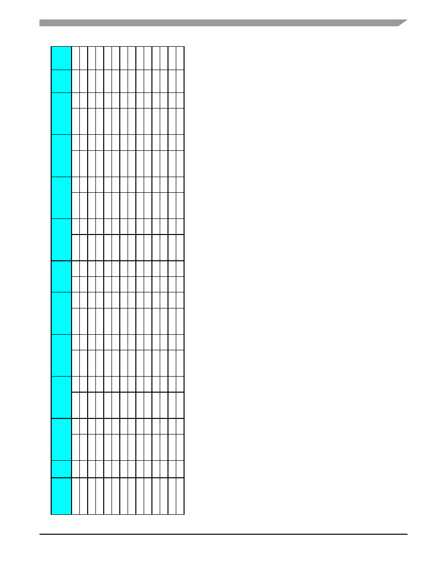
i.MX31/i.MX31L A
d
v
a
nce
In
f
o
rmat
ion
, Re
v
. 1.4
Fre
e
scale Semico
nductor
55
Preli
m
i
nar
y
Si
gn
al
D
e
sc
r
ip
t
io
ns
NGND2
≠
≠
≠
≠
≠
≠
≠
≠
≠
≠
≠
≠
≠
≠
≠
≠
≠
≠
≠
≠
NA
NGND3
≠
≠
≠
≠
≠
≠
≠
≠
≠
≠
≠
≠
≠
≠
≠
≠
≠
≠
≠
≠
NA
NGND4
≠
≠
≠
≠
≠
≠
≠
≠
≠
≠
≠
≠
≠
≠
≠
≠
≠
≠
≠
≠
NA
NGND5
≠
≠
≠
≠
≠
≠
≠
≠
≠
≠
≠
≠
≠
≠
≠
≠
≠
≠
≠
≠
NA
NGND6
≠
≠
≠
≠
≠
≠
≠
≠
≠
≠
≠
≠
≠
≠
≠
≠
≠
≠
≠
≠
NA
NGND7
≠
≠
≠
≠
≠
≠
≠
≠
≠
≠
≠
≠
≠
≠
≠
≠
≠
≠
≠
≠
NA
NGND8
≠
≠
≠
≠
≠
≠
≠
≠
≠
≠
≠
≠
≠
≠
≠
≠
≠
≠
≠
≠
NA
NGND9
≠
≠
≠
≠
≠
≠
≠
≠
≠
≠
≠
≠
≠
≠
≠
≠
≠
≠
≠
≠
NA
NGND10
≠
≠
≠
≠
≠
≠
≠
≠
≠
≠
≠
≠
≠
≠
≠
≠
≠
≠
≠
≠
NA
NGND21
≠
≠
≠
≠
≠
≠
≠
≠
≠
≠
≠
≠
≠
≠
≠
≠
≠
≠
≠
≠
NA
NGND22
≠
≠
≠
≠
≠
≠
≠
≠
≠
≠
≠
≠
≠
≠
≠
≠
≠
≠
≠
≠
NA
QVCC
≠
≠
≠
≠
≠
≠
≠
≠
≠
≠
≠
≠
≠
≠
≠
≠
≠
≠
≠
≠
NA
QVCC1
≠
≠
≠
≠
≠
≠
≠
≠
≠
≠
≠
≠
≠
≠
≠
≠
≠
≠
≠
≠
NA
QVCC4
≠
≠
≠
≠
≠
≠
≠
≠
≠
≠
≠
≠
≠
≠
≠
≠
≠
≠
≠
≠
NA
Table 6. Pad Settings (continued)
Pin Name
Pad
Slew Rate
Loopback
Drive Strength
Enable (Max)
Drive Strength
Enable0 (High/
Normal)
Pull Value
Pull/
Keep
Select
Pull/
Keep Enable
Open
Drain
Schmitt Trigger
Supply
Group
Value
After
Reset
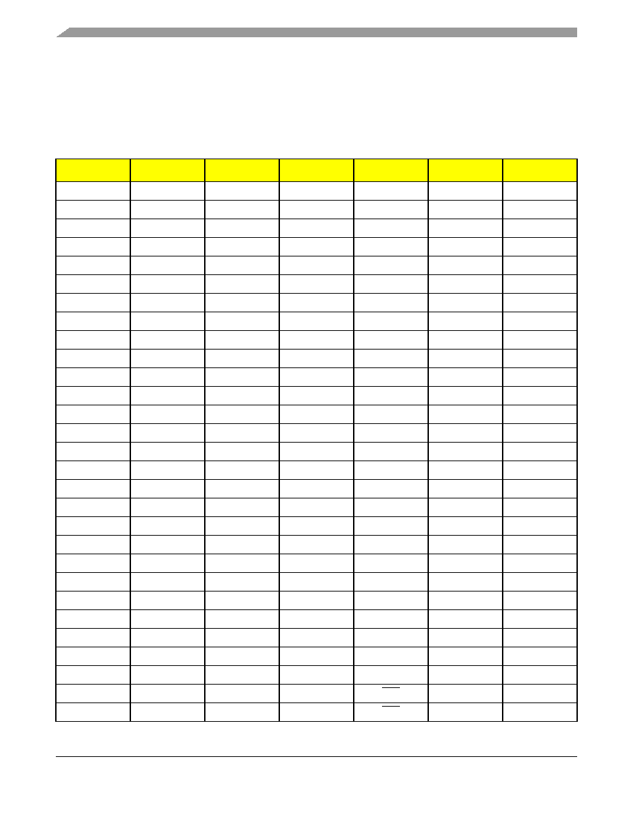
i.MX31/i.MX31L Advance Information, Rev. 1.4
56
Freescale Semiconductor
Preliminary
Signal Descriptions
3.1.3
EMI Pins Multiplexing
This section discusses the multiplexing of EMI signals. The EMI signals' multiplexing is done inside the
EMI.
Table 7
lists the i.MX31 and i.MX31L pin names, pad types, and the memory devices' equivalent pin
names.
Table 7. EMI Multiplexing
Pin Name
Pad Type
WEIM
SDRAM
PCMCIA
DDR
NFC
A0
regular
A0
MA0
A0
MA0
≠
A1
regular
A1
MA1
A1
MA1
≠
A2
regular
A2
MA2
A2
MA2
≠
A3
regular
A3
MA3
A3
MA3
≠
A4
regular
A4
MA4
A4
MA4
≠
A5
regular
A5
MA5
A5
MA5
≠
A6
regular
A6
MA6
A6
MA6
≠
A7
regular
A7
MA7
A7
MA7
≠
A8
regular
A8
MA8
A8
MA8
≠
A9
regular
A9
MA9
A9
MA9
≠
A10
regular
A10
≠
A10
≠
≠
MA10
regular
≠
MA10
≠
MA10
≠
A11
regular
A11
MA11
A11
MA11
≠
A12
regular
A12
MA12
A12
MA12
≠
A13
regular
A13
MA13
A13
MA13
≠
A14
regular
A14
≠
A14
≠
≠
A15
regular
A15
≠
A15
≠
≠
A16
regular
A16
≠
A16
≠
≠
A17
regular
A17
≠
A17
≠
≠
A18
regular
A18
≠
A18
≠
≠
A19
regular
A19
≠
A19
≠
≠
A20
regular
A20
≠
A20
≠
≠
A21
regular
A21
≠
A21
≠
≠
A22
regular
A22
≠
A22
≠
≠
A23
regular
A23
≠
A23
≠
≠
A24
regular
A24
≠
A24
≠
≠
A25
regular
A25
≠
A25
≠
≠
SDBA1
regular
SDBA1
≠
CE1
≠
≠
SDBA0
regular
SDBA0
≠
CE2
≠
≠
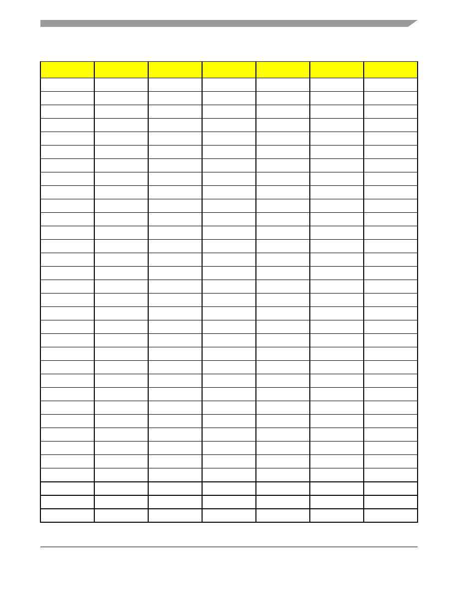
Signal Descriptions
i.MX31/i.MX31L Advance Information, Rev. 1.4
Freescale Semiconductor
57
Preliminary
SD0
ddr
≠
SD0
≠
≠
≠
SD1
ddr
≠
SD1
≠
≠
≠
SD2
ddr
≠
SD2
≠
≠
≠
SD3
ddr
≠
SD3
≠
≠
≠
SD4
ddr
≠
SD4
≠
≠
≠
SD5
ddr
≠
SD5
≠
≠
≠
SD6
ddr
≠
SD6
≠
≠
≠
SD7
ddr
≠
SD7
≠
≠
≠
SD8
ddr
≠
SD8
≠
≠
≠
SD9
ddr
≠
SD9
≠
≠
≠
SD10
ddr
≠
SD10
≠
≠
≠
SD11
ddr
≠
SD11
≠
≠
≠
SD12
ddr
≠
SD12
≠
≠
≠
SD13
ddr
≠
SD13
≠
≠
≠
SD14
ddr
≠
SD14
≠
≠
≠
SD15
ddr
≠
SD15
≠
≠
≠
SD16
ddr
≠
SD16
≠
≠
≠
SD17
ddr
≠
SD17
≠
≠
≠
SD18
ddr
≠
SD18
≠
≠
≠
SD19
ddr
≠
SD19
≠
≠
≠
SD20
ddr
≠
SD20
≠
≠
≠
SD21
ddr
≠
SD21
≠
≠
≠
SD22
ddr
≠
SD22
≠
≠
≠
SD23
ddr
≠
SD23
≠
≠
≠
SD24
ddr
≠
SD24
≠
≠
≠
SD25
ddr
≠
SD25
≠
≠
≠
SD26
ddr
≠
SD26
≠
≠
≠
SD27
ddr
≠
SD27
≠
≠
≠
SD28
ddr
≠
SD28
≠
≠
≠
SD29
ddr
≠
SD29
≠
≠
≠
SD30
ddr
≠
SD30
≠
≠
≠
SD31
ddr
≠
SD31
≠
≠
≠
DQM0
ddr
≠
DQM0
≠
≠
≠
Table 7. EMI Multiplexing (continued)
Pin Name
Pad Type
WEIM
SDRAM
PCMCIA
DDR
NFC
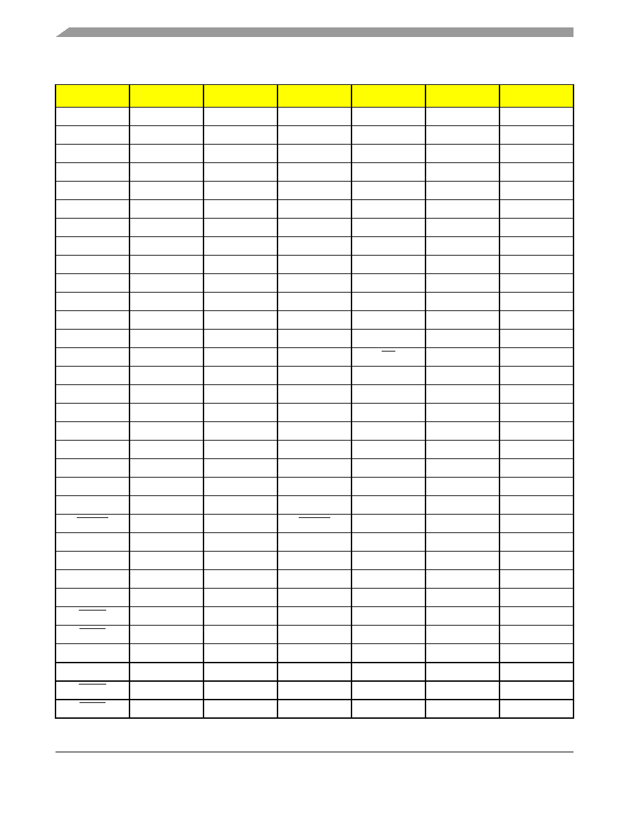
i.MX31/i.MX31L Advance Information, Rev. 1.4
58
Freescale Semiconductor
Preliminary
Signal Descriptions
DQM1
ddr
≠
DQM1
≠
≠
≠
DQM2
ddr
≠
DQM2
≠
≠
≠
DQM3
ddr
≠
DQM3
≠
≠
≠
EB0
regular
EB0
≠
REG
≠
≠
EB1
regular
EB1
≠
IORD
≠
≠
OE
regular
OE
≠
IOWR
≠
≠
CS0
regular
CS0
≠
≠
≠
≠
CS1
regular
CS1
≠
≠
≠
≠
CS2
regular
CS2
CSD0
≠
≠
≠
CS3
regular
CS3
CSD1
≠
≠
≠
CS4
regular
CS4
≠
≠
≠
≠
CS5
regular
CS5
≠
≠
≠
≠
ECB
regular
ECB
≠
≠
≠
≠
LBA
regular
LBA
≠
OE
≠
≠
BCLK
regular
BCLK
≠
≠
≠
≠
RW
regular
RW
≠
WE
≠
≠
RAS
regular
≠
RAS
≠
≠
≠
CAS
regular
≠
CAS
≠
≠
≠
SDWE
regular
≠
SDWE
≠
≠
≠
SDCKE0
regular
≠
SDCKE0
≠
≠
≠
SDCKE1
regular
≠
SDCKE1
≠
≠
≠
SDCLK
ddr
≠
SDCLK
≠
≠
≠
SDCLK
ddr
≠
SDCLK
≠
≠
≠
SDQS0
ddr
≠
≠
≠
SDQS0
≠
SDQS1
ddr
≠
≠
≠
SDQS1
≠
SDQS2
ddr
≠
≠
≠
SDQS2
≠
SDQS3
ddr
≠
≠
≠
SDQS3
≠
NFWE
regular
≠
≠
≠
≠
WE
NFRE
regular
≠
≠
≠
≠
RE
NFALE
regular
≠
≠
≠
≠
ALE
NFCLE
regular
≠
≠
≠
≠
CLE
NFWP
regular
≠
≠
≠
≠
WP
NFCE
regular
≠
≠
≠
≠
CE
Table 7. EMI Multiplexing (continued)
Pin Name
Pad Type
WEIM
SDRAM
PCMCIA
DDR
NFC
Signal Descriptions
i.MX31/i.MX31L Advance Information, Rev. 1.4
Freescale Semiconductor
59
Preliminary
NFRB
regular
≠
≠
≠
≠
R/B
D15
regular
D15
≠
D15
≠
D15
D14
regular
D14
≠
D14
≠
D14
D13
regular
D13
≠
D13
≠
D13
D12
regular
D12
≠
D12
≠
D12
D11
regular
D11
≠
D11
≠
D11
D10
regular
D10
≠
D10
≠
D10
D9
regular
D9
≠
D9
≠
D9
D8
regular
D8
≠
D8
≠
D8
D7
regular
D7
≠
D7
≠
D7
D6
regular
D6
≠
D6
≠
D6
D5
regular
D5
≠
D5
≠
D5
D4
regular
D4
≠
D4
≠
D4
D3
regular
D3
≠
D3
≠
D3
D2
regular
D2
≠
D2
≠
D2
D1
regular
D1
≠
D1
≠
D1
D0
regular
D0
≠
D0
≠
D0
PC_CD1
regular
≠
≠
CD1
≠
≠
PC_CD2
regular
≠
≠
CD2
≠
≠
PC_WAIT
regular
≠
≠
WAIT
≠
≠
PC_READY
regular
≠
≠
READY
≠
≠
PC_PWRON
regular
≠
≠
PC_PWRON
≠
≠
PC_VS1
regular
≠
≠
VS1
≠
≠
PC_VS2
regular
≠
≠
VS2
≠
≠
PC_BVD1
regular
≠
≠
BVD1
≠
≠
PC_BVD2
regular
≠
≠
BVD2
≠
≠
PC_RST
regular
≠
≠
RST
≠
≠
IOIS16
regular
≠
≠
IOIS16/WP
≠
≠
PC_RW
regular
≠
≠
RW
≠
≠
PC_POE
regular
≠
≠
POE
≠
≠
M_REQUEST
regular
≠
≠
≠
≠
≠
M_GRANT
regular
≠
≠
≠
≠
≠
Table 7. EMI Multiplexing (continued)
Pin Name
Pad Type
WEIM
SDRAM
PCMCIA
DDR
NFC

i.MX31/i.MX31L Advance Information, Rev. 1.4
60
Freescale Semiconductor
Preliminary
Electrical Characteristics
4
Electrical Characteristics
This section provides the chip-level and module-level electrical characteristics for the i.MX31 and
i.MX31L:
∑
Section 4.1, "i.MX31 and i.MX31L Chip-Level Conditions
"
on page 60
--
Section 4.1.1, "Power Specifications
"
on page 63
∑
Section 4.2, "Supply Power-Up Requirements and Restrictions
"
on page 66
∑
Section 4.3, "Module-Level Electrical Specifications
"
on page 66
--
Section 4.3.1, "I/O Pad (PADIO) Electrical Specifications
"
on page 66
--
Section 4.3.3, "Clock Amplifier Module (CAMP) Electrical Characteristics
"
on page 70
--
Section 4.3.4, "1-Wire Electrical Specifications
"
on page 70
--
Section 4.3.5, "ATA Electrical Specifications (ATA Bus, Bus Buffers)
"
on page 72
--
Section 4.3.6, "AUDMUX Electrical Specifications
"
on page 80
--
Section 4.3.7, "CSPI Electrical Specifications
"
on page 80
--
Section 4.3.8, "DPLL Electrical Specifications
"
on page 82
--
Section 4.3.9, "EMI Electrical Specifications
"
on page 83
≠
Section 4.3.9.1, "NAND Flash Controller Interface (NFC)
"
on page 83
≠
Section 4.3.9.2, "Wireless External Interface Module (WEIM)
"
on page 88
≠
Section 4.3.9.3, "SDRAM (DDR and SDR) Memory Controller
"
on page 93
--
Section 4.3.11, "FIR Electrical Specifications
"
on page 101
--
Section 4.3.12, "Fusebox Electrical Specifications
"
on page 101
--
Section 4.3.13, "I2C Electrical Specifications
"
on page 102
--
Section 4.3.14, "IPU--Sensor Interfaces
"
on page 106
--
Section 4.3.15, "IPU--Display Interfaces
"
on page 106
--
Section 4.3.16, "Memory Stick Host Controller (MSHC)
"
on page 131
--
Section 4.3.17, "Personal Computer Memory Card International Association (PCMCIA)
"
on
page 133
--
Section 4.3.18, "PWM Electrical Specifications
"
on page 135
--
Section 4.3.19, "SDHC Electrical Specifications
"
on page 137
--
Section 4.3.20, "SIM Electrical Specifications
"
on page 138
--
Section 4.3.21, "SJC Electrical Specifications
"
on page 141
--
Section 4.3.22, "SSI Electrical Specifications
"
on page 143
--
Section 4.3.23, "USB Electrical Specifications
"
on page 151
4.1
i.MX31 and i.MX31L Chip-Level Conditions
This section provides the chip-level electrical characteristics for the IC. See
Table 8
for a quick reference
to the individual tables and sections.
Electrical Characteristics
i.MX31/i.MX31L Advance Information, Rev. 1.4
Freescale Semiconductor
61
Preliminary
Table 9
provides the DC recommended operating conditions.
NOTE
The use of the terms OVDD and OVSS in this section refers to VDD/VSS
Power rails of I/O pads, which are supplied by the nearest noisy (V
DDIOL/H
and V
DD_DDR
) supply pads, and are in the range of 1.75 to 3.1 V.
Table 8. i.MX31/i.MX31L Chip-Level Conditions
For these characteristics, ...
Topic appears ...
Table 9, "DC Recommended Operating Conditions"
on page 61
Table 10, "Voltage versus Core Frequency"
on page 62
Table 11, "Interface Frequency"
on page 62
Table 12, "DC Absolute Maximum Operating Conditions"
on page 63
Section 4.1.1, "Power Specifications"
on page 63
Table 9. DC Recommended Operating Conditions
ID
Parameter
Symbol
Min
Max
Units
1
Core Supply Voltage
1,
2
(QVCC, QVCC1, QVCC4)
1
Measured at supply pins, including peripherals, ARM, and L2 cache supplies (QVCC, QVCC1, QVCC4, respectively).
2
Min voltage listed is for the lower frequency. See
Table 10
for correlation of voltage range and associated frequencies.
V
DD
1.22
1.65
3
3
Core voltage supply is considered "Overdrive" for 1.45≠1.65 V range. Duty cycles in core overdrive--whether switching or
not--must be limited to a cumulative duration of 1.25 years or less (25% duty cycle for a 5-year rated part) to sustain a
maximum core VDD operating voltage of 1.65 V without significant device degradation.
V
2
State Retention (SR) Operating Voltage
4
4
The SR voltage (Quiet supplies QVCC, QVCC1, QVCC4), is applied after IC is put in SR mode. NOTE: Applying low voltage
point is dependent on noisy (NVCC) supplies being less than or equal to 1.95 V.
V
SR
0.95
≠
V
3
I/O Supply Voltage
NVCC1, NVCC3, NVCC4-10
V
DDIOL
1.75
1.9
V
4
I/O Supply Voltage
NVCC1, NVCC3, NVCC4-10
V
DDIOH
2.7
5
5
The range--1.9 V to 2.7 V--is a valid voltage range; however, the voltage ranges given in this table align to more common
industry voltage ranges.
3.1
6,7,8
V
5
Supply Voltage (DDR Output Drive Supply)
NVCC2, NVCC21, NVCC22
V
DD_DDR
1.75
1.95
V
6
PLL/FPM supplies: FVCC, MVCC, SVCC, UVCC
9
V
PLL
1.3
1.6
V
7
Fusebox read Supply Voltage on the VDD_FUSE pin
V
FUSE
1.65
1.95
V
8
Fusebox Program Supply Voltage on the VDD_FUSE pin
10
V
FUSE_PGM
3.0
3.3
V
9
Operating Ambient Temperature
T
A
0
70
o
C
i.MX31/i.MX31L Advance Information, Rev. 1.4
62
Freescale Semiconductor
Preliminary
Electrical Characteristics
Table 10
gives details of the applied voltages to the i.MX31/i.MX31L Core Supply I/O versus the
frequencies of the ARM11 core.
Table 11
provides information for interface frequency limits. For more details about clocks characteristics,
see
Section 4.3.8, "DPLL Electrical Specifications
"
on page 82
.
Table 12
provides the DC absolute maximum operating conditions.
CAUTION
Stresses beyond those listed under
"DC Absolute Maximum Operating
Conditions,"
(
Table 12
) may cause permanent damage to the device. These
are stress ratings only. Functional operation of the device at these or any
other conditions beyond those indicated under "recommended operating
conditions" is not implied. Exposure to absolute-maximum-rated conditions
for extended periods may affect device reliability.
6
Recommended maximum OVDD operating voltage is 3.1 V for GPIO in either slow or fast mode. Switching duty cycles must
be limited to a cumulative duration of 1 year or less (20% duty cycle for a 5yr rated part) to sustain a MAX OVDD operating
voltage of 3.3V without significant device degradation. A switching cycle is defined as the period of time that the pad is powered
to OVDD and actively switching. Switching cycles exceeding this limit may affect device performance or cause permanent
damage to the device.
7
The performance at 1.8 V of GPIO devices that are operated at 3.3 V over an extended period of time (for example. 2 years or
longer at a 20% duty cycle) is not guaranteed. Reliability degradation may render the device too slow or inoperable.
8
Overshoot and undershoot conditions (transitions above OVDD and below OVSS) on switching pads must be held below 0.6 V,
and the duration of the overshoot/undershoot must not exceed 10% of the system clock cycle. Overshoot/undershoot must be
controlled through printed circuit board layout, transmission line impedance matching, signal line termination, or other methods.
Non-compliance to this specification may affect device reliability or cause permanent damage to the device.
9
For normal operating conditions, PLLs' and core supplies must maintain the following relation: PLL
Core ≠ 100 mV. In other
words, for a 1.6 V core supply, PLL supplies must be set to 1.5 V or higher.
10
Providing a voltage that is lower than specified does not prevent the fuses from being blown if attempting to program a fuse.
Table 10. Voltage versus Core Frequency
ID
Core
Symbol
Min (V)
Max (V)
Frequency (MHz)
1
ARM11 (V
DD
)
f
ARM
1.22
1
1
As measured at the ball. Recommended settings for PMIC (Power Management IC) is 1.275 V.
1.65
1, 2
2
All overdrive/25% duty-cycles restrictions apply, as specified in
Table 9
.
0≠400
2
f
ARM
1.55
3
3
As measured at the ball. Recommended voltage settings for PMIC is 1.6 V.
1.65
3
401≠532
Table 11. Interface Frequency
ID
Parameter
Symbol
Min
Typ
Max
Units
1
JTAG TCK Frequency
f
JTAG
DC
5
10
MHz
2
CKIL Frequency
f
CKIL
32
32.768
38.4
kHz
3
CKIH Frequency
f
CKIH
10
26
100
MHz
Electrical Characteristics
i.MX31/i.MX31L Advance Information, Rev. 1.4
Freescale Semiconductor
63
Preliminary
4.1.1
Power Specifications
Table 13
shows the power consumption for the i.MX31 and i.MX31L.
Table 12. DC Absolute Maximum Operating Conditions
Ref. Num
Parameter
Symbol
Min
Max
Units
1
Supply Voltage
V
DDmax
-0.5
1.65
V
2
Supply Voltage (Level Shift I/O)
V
DDIOmax
-0.5
3.3
V
3
Input Voltage Range
V
Imax
-0.5
V
DDIOH
+0.3
V
4
Storage Temperature
T
storage
-40
125
o
C
5
Absolute Maximum HBM (Human Body Model) ESD stress
voltage.
V
esd
≠
±
2500
V
6
Absolute Maximum offset voltage allowed in run mode
between core supplies.
V
coers_offset
1
1
The offset is any difference between all core voltages for supply pads--QVCC, QVCC1, and QVCC4.
≠
+15
mV

i.MX31/i.MX31L Advance Information, Rev. 1.4
64
Freescale Semiconductor
Preliminary
Electrical Characteristics
Table 13. Power Consumption (Typical Values)
Mode
Conditions
Peripheral
Current
1
ARM
Current
2
PLL
Current
Total Power
State Retention ∑ Core VDD (QVCC) = 0.95 V
∑ ARM supply QVCC1 = QVCC = 0.95 V
∑ ARM in well bias
∑ L2 caches are power gated (QVCC4 = 0 V)
∑ All PLLs are Off
∑ FPM is off
∑ 32 kHz Input on
∑ CKIH input is off
∑ CAMP is off
∑ TCK input is off
∑ All the modules are off
∑ No external resistive loads
∑ RNGA oscillator is off
∑ T
A
= 25∫C
200
µA
150
µA
40
µA
0.4 mW
Doze
∑ All Vdds = 1.2 V (QVCC=QVCC1= QVCC4 = 1.2 V)
∑ ARM in wait for interrupt mode
∑ ARM is in well bias
∑ MAX is stopped
∑ L2 cache is stopped but powered
∑ MCU PLL is on (532 MHz)
∑ USB PLL and SPLL are off
∑ FPM is on
∑ CKIH input is off
∑ CAMP is off
∑ 32 kHz Input on
∑ All the modules are off (by programming CGR[2:0]
registers)
∑ RNGA oscillator is off
∑ No external resistive loads
∑ T
A
= 25∫C
7 mA
1.0 mA
3 mA for
each
PLL
13.0 mW
Electrical Characteristics
i.MX31/i.MX31L Advance Information, Rev. 1.4
Freescale Semiconductor
65
Preliminary
4.2
Supply Power-Up Requirements and Restrictions
Any i.MX31/i.MX31L board design must comply with the power-up sequence guideline, as described in
this section, to guarantee proper power-up of the device. Any deviation from this sequence may result in
any or all of the following situations:
∑
Cause excessive current.
∑
Prevent the device from booting.
∑
Cause irreversible damage to the i.MX31/i.MX31L (worst-case scenario).
The Power On Reset (POR) pin must be kept asserted (low) throughout the power up sequence. Power up
logic must guarantee that all power sources must be on prior to the release (de-assertion) of POR.
Figure 2
depicts the power supply power up sequence. (Power management logic should guarantee 90% supply
before transitional to the next state.) The sequence is as follows:
1. Quiet supplies--QVCC, QVCC1, QVCC4 (peripherals, ARM, L2 cache)
2. NVCC1 and IOQVDD--for assuring reset signals are propagating into core
WAIT (all clocks
gated off)
∑ All Vdds = 1.2 V (QVCC=QVCC1=QVCC4 = 1.2 V)
∑ ARM in wait for interrupt mode
∑ MAX is active
∑ L2 cache is stopped but powered
∑ MCU PLL is on (532 MHz)
∑ USB PLL and SPLL are off
∑ FPM is on
∑ CKIH input is off
∑ CAMP is off
∑ 32 kHz Input on
∑ All the modules are off (by programming CGR[2:0]
registers)
∑ RNGA oscillator is off
∑ No external resistive loads
∑ T
A
= 25∫C
7 mA
3 mA
3 mA for
each
PLL
15.0 mW
Deep Sleep
∑ Core VDD (QVCC) = 0.95 V
∑ ARM (QVCC1) & L2 caches (QVCC4) are power gate
∑ All PLLs are off
∑ FPM is off
∑ 32 kHz Input on
∑ CKIH input is off
∑ CAMP is off
∑ TCK input is off
∑ All the modules are off
∑ No external resistive loads
∑ RNGA oscillator is off
∑ T
A
= 25∫C
200
µA
0
µA
40
µA
0.22 mW
1
QVCC supply.
2
QVCC1 supply.
Table 13. Power Consumption (Typical Values) (continued)
Mode
Conditions
Peripheral
Current
1
ARM
Current
2
PLL
Current
Total Power
i.MX31/i.MX31L Advance Information, Rev. 1.4
66
Freescale Semiconductor
Preliminary
Electrical Characteristics
3. Powering up of the remainder of noisy and PLL supplies, which can be done simultaneously. The
order within the noisy supplies must be maintained, as follows:
a) Remainder of noisy supplies (all except for the NVCC2, 21,22, and NVCC1 supplies)
b) NVCC2, NVCC21, NVCC22.
4. FUSE_VDD--the last supply to be powered up
Figure 2. Power-Up Sequence
4.3
Module-Level Electrical Specifications
This section contains the i.MX31 and i.MX31L electrical information including timing specifications,
arranged in alphabetical order by module name.
4.3.1
I/O Pad (PADIO) Electrical Specifications
This section specifies the AC/DC characterization of functional I/O pads of the i.MX31. There are two
main types of pads: regular and DDR. In this document, the "Regular" type is referred to as GPIO.
4.3.1.1
DC Electrical Characteristics
The i.MX31/i.MX31L pad I/O operating characteristics appear in
Table 14
for GPIO pads and
Table 15
for DDR (Double Data Rate) pads.
QVCC, QVCC1, QVCC4
NVCC1,
IOQVDD
Remainder of Noisy Supplies--
V
DDIOL/H
NVCC2,
NVCC21, 22
FUSE_VDD
Hold POR Asserted
Release POR
PLL's
Supplies
Electrical Characteristics
i.MX31/i.MX31L Advance Information, Rev. 1.4
Freescale Semiconductor
67
Preliminary
Table 14. GPIO Pads DC Electrical Parameters
Parameter
Symbol
Test Conditions
Min
Typ
Max
Units
High-level output voltage
V
OH
I
OH
= ≠1 mA
OVDD
≠0.15
1
1
Power rail for output driver 1.75 - 3.1 V.
≠
≠
V
I
OH
= spec'ed Drive
0.8*OVDD
≠
≠
V
Low-level output voltage
V
OL
I
OL
= 1 mA
≠
≠
0.15
VV
I
OL
= spec'ed Drive
≠
≠
0.2*OVDD
High-level output current, slow slew rate
2
2
Tested per I/O pad.
I
OH_S
V
OH
=0.8*OVDD
Std Drive
High Drive
Max Drive
≠2
≠4
≠8
≠
≠
mA
High-level output current, fast slew rate
2
I
OH_F
V
OH
=0.8*OVDD
Std Drive
High Drive
Max Drive
≠4
≠6
≠8
≠
≠
mA
Low-level output current, slow slew rate
2
I
OL_S
V
OL
=0.2*OVDD
Std Drive
High Drive
Max Drive
2
4
8
≠
≠
mA
Low-level output current, fast slew rate
2
I
OL_F
V
OL
=0.2*OVDD
Std Drive
High Drive
Max Drive
4
6
8
≠
≠
mA
High-Level DC input voltage
3
3
V
IH
, V
IL
,V
T+
and V
T-
for the pads in supply groups NVCC3-NVCC10 are referenced to OVDD.
V
IH
≠
0.7*OVDD
≠
OVDD
V
Low-Level DC input voltage
3
V
IL
≠
0
≠
0.3*VDD
V
Input Hysteresis
V
HYS
≠
0.25
≠
≠
V
Schmitt trigger VT+
1, 4
4
Hysteresis of 250 mV is guaranteed over all operating conditions when hysteresis is enabled.
V
T
+
≠
0.5*VDD
≠
≠
V
Schmitt trigger VT-
V
T
-
≠
≠
≠
0.5*VDD
V
Pull-up resistor (100 K
PU)
R
PU
≠
70
100
268
K
Pull-down resistor (100 K
PD)
R
PD
≠
61
100
343
Input current (no PU/PD)
5
5
Typ condition: typ model, 1.875 V and 25∞C. Max condition: bcs model, 3.3 V and 105∞C.
I
IN
V
I
= 0
V
I
= OVDD
≠
0.33
250
100
nA
Input current (100 K
PU)
I
IN
V
I
= 0
V
I
= OVDD
≠
≠
25
0.1
µA
µA
Input current (100 K
PD)
I
IN
V
I
= 0
V
I
= OVDD
≠
≠
0.25
28
µA
µA
Tri-state Hi-Z input current
I
Z
V
I
= OVDD or 0
≠
≠
2
µA
i.MX31/i.MX31L Advance Information, Rev. 1.4
68
Freescale Semiconductor
Preliminary
Electrical Characteristics
4.3.2
AC Electrical Characteristics
Figure 3
depicts the load circuit for output pads.
Figure 4
depicts the output pad transition time waveform.
The range of operating conditions appears in
Table 16
for slow general I/O,
Table 17
for fast general I/O,
and
Table 18
for DDR I/O (unless otherwise noted).
Figure 3. Load Circuit for Output Pad
Table 15. DDR (Double Data Rate) I/O Pads DC Electrical Parameters
Parameter
Symbol
Test Conditions
Min
Typ
Max
Units
High-level output voltage
1
1
Max operating voltage for DDR pads with all drive strengths is 1.95 V.
V
OH
I
OH
= ≠1 mA
OVDD ≠0.12
≠
≠
V
I
OH
= spec'ed Drive
0.8*OVDD
≠
≠
V
Low-level output voltage
V
OL
I
OL
= 1 mA
≠
≠
0.08
V
I
OL
= spec'ed Drive
≠
≠
0.2*OVDD
V
High-level output current
2
2
Tested per I/O pad.
I
OH
V
OH
=0.8*OVDD
Std Drive
High Drive
Max Drive
DDR Drive
≠3.6
≠7.2
≠10.8
≠14.4
≠
≠
mA
Low-level output current
2
I
OL
V
OL
=0.2*OVDD
Std Drive
High Drive
Max Drive
DDR Drive
3.6
7.2
10.8
14.4
≠
≠
mA
High-Level DC input voltage of CMOS receiver
V
IH
≠
0.7*OVDD
OVDD OVDD+0.3
V
Low-Level DC input voltage of CMOS receiver
V
IL
≠
≠0.3
0
0.3*OVDD
V
Low-level input current
3
3
Input current conditions: Typical condition: typ model, 1.875 V and 25∞C. Max condition: bcs model, 3.3 V and 105∞C
I
IL
V
I
= 0
≠
≠
900
nA
High-level input current
I
IH
V
I
= OVDD
≠
≠
140
nA
Tri-state Hi-Z current
I
Z
V
I
= OVDD or 0
≠
≠
2
µA
Test Point
From Output
Under Test
CL
CL includes package, probe and jig capacitance
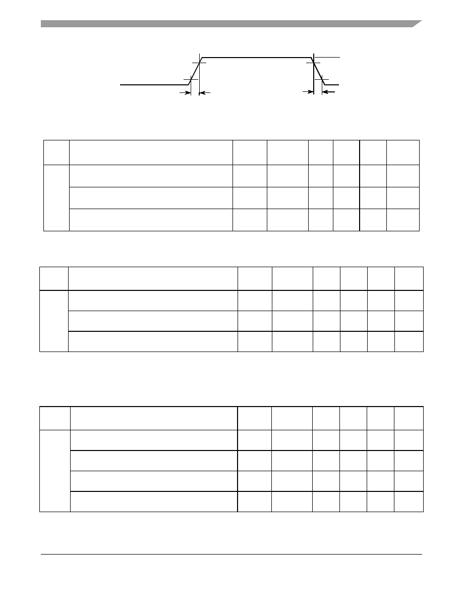
Electrical Characteristics
i.MX31/i.MX31L Advance Information, Rev. 1.4
Freescale Semiconductor
69
Preliminary
Figure 4. Output Pad Transition Time Waveform
Table 16. AC Electrical Characteristics of Slow
1
General I/O Pads
1
Fast/slow characteristic is selected per GPIO I/O pad (where available) by "slew rate" control. See
Table 6
.
ID
Parameter
Symbol
Test
Condition
Min
Typ
Max
Units
PA1
Output Pad Transition Times (Max Drive)
tpr
25 pF
50 pF
0.92
1.5
1.95
2.98
3.17
4.75
ns
Output Pad Transition Times (High Drive)
tpr
25 pF
50 pF
1.52
2.75
4.81
8.42
ns
Output Pad Transition Times (Std Drive)
tpr
25 pF
50 pF
2.79
5.39
8.56
16.43
ns
Table 17. AC Electrical Characteristics of Fast
1
General I/O Pads
2
1
Fast/slow characteristic is selected per GPIO I/O pad (where available) by "slew rate" control. See
Table 6
.
2
Recommended max operating voltage for GPIO in fast mode with all drive strengths is 1.95 V. Absolute maximum is described
in
Table 9
.
ID
Parameter
Symbol
Test
Condition
Min
Typ
Max
Units
PA1
Output Pad Transition Times (Max Drive)
tpr
25 pF
50 pF
0.68
1.34
1.33
2.6
2.07
4.06
ns
Output Pad Transition Times (High Drive)
tpr
25 pF
50 pF
.91
1.79
1.77
3.47
2.74
5.41
ns
Output Pad Transition Times (Std Drive)
tpr
25 pF
50 pF
1.36
2.68
2.64
5.19
4.12
8.11
ns
Table 18. AC Electrical Characteristics of DDR I/O Pads
1
1
Absolute max operating voltage for DDR pads with all drive strengths is 1.95 V.
ID
Parameter
Symbol
Test
Condition
Min
Typ
Max
Units
PA1
Output Pad Transition Times (DDR Drive)
tpr
25 pF
50 pF
0.51
0.97
0.82
1.58
1.28
2.46
ns
Output Pad Transition Times (Max Drive)
tpr
25 pF
50 pF
0.67
1.29
1.08
2.1
1.69
3.27
ns
Output Pad Transition Times (High Drive)
tpr
25 pF
35 pF
.99
1.93
1.61
3.13
2.51
4.89
ns
Output Pad Transition Times (Std Drive)
tpr
25 pF
50 pF
1.96
3.82
3.19
6.24
4.99
9.73
ns
0V
OVDD
20%
80%
80%
20%
PA1
PA1
Output (at pad)
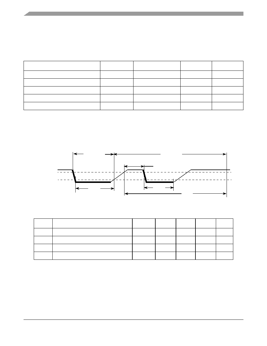
i.MX31/i.MX31L Advance Information, Rev. 1.4
70
Freescale Semiconductor
Preliminary
Electrical Characteristics
4.3.3
Clock Amplifier Module (CAMP) Electrical Characteristics
This section outlines the Clock Amplifier Module (CAMP) specific electrical characteristics.
Table 19
shows clock amplifier electrical characteristics.
4.3.4
1-Wire Electrical Specifications
Figure 5
depicts the RPP timing, and
Table 20
lists the RPP timing parameters.
Figure 5. Reset and Presence Pulses (RPP) Timing Diagram
Figure 6
depicts Write 0 Sequence timing, and
Table 21
lists the timing parameters.
Table 19. Clock Amplifier Electrical Characteristics
Parameter
Min
Typ
Max
Units
Input Frequency
8.0
≠
34.0
MHz
VIL (for square input)
0
≠
0.3
V
VIH (for square input)
(VDD
1
- 0.25)
1
VDD is the supply voltage of CAMP
≠
3
V
Sinusoidal Input Amplitude
0.4
2
2
This value of the sinusoidal input will be measured through characterization.
≠
VDD
Vp-p
Duty Cycle
45
50
55
%
Table 20. RPP Sequence Delay Comparisons Timing Parameters
ID
Parameters
Symbol
Min
Typ
Max
Units
OW1
Reset Time Low
t
RSTL
480
511
≠
µs
OW2
Presence Detect High
t
PDH
15
≠
60
µs
OW3
Presence Detect Low
t
PDL
60
≠
240
µs
OW4
Reset Time High
t
RSTH
480
512
≠
µs
1-Wire bus
DS2502 Tx
"Presence Pulse"
(BATT_LINE)
OWIRE Tx
"Reset Pulse"
OW1
OW2
OW3
OW4
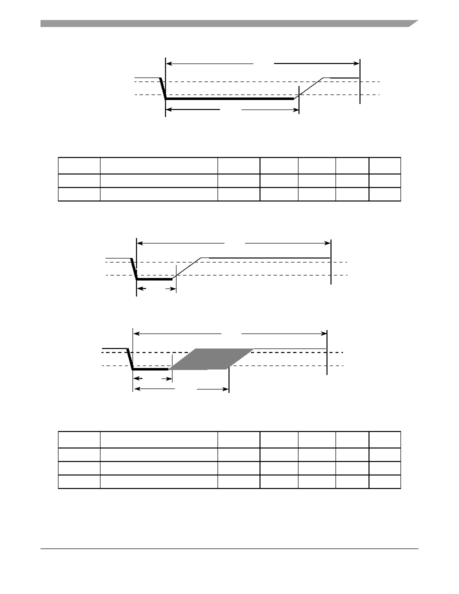
Electrical Characteristics
i.MX31/i.MX31L Advance Information, Rev. 1.4
Freescale Semiconductor
71
Preliminary
Figure 6. Write 0 Sequence Timing Diagram
Figure 7
depicts Write 1 Sequence timing,
Figure 8
depicts the Read Sequence timing, and
Table 22
lists
the timing parameters.
Figure 7. Write 1 Sequence Timing Diagram
Figure 8. Read Sequence Timing Diagram
Table 21. WR0 Sequence Timing Parameters
ID
Parameter
Symbol
Min
Typ
Max
Units
OW5
Write 0 Low Time
t
WR0_low
60
100
120
µs
OW6
Transmission Time Slot
t
SLOT
OW5
117
120
µs
Table 22. WR1 /RD Timing Parameters
ID
Parameter
Symbol
Min
Typ
Max
Units
OW7
Write 1 / Read Low Time
t
LOW1
1
5
15
µs
OW8
Transmission Time Slot
t
SLOT
60
117
120
µs
OW9
Release Time
t
RELEASE
15
≠
45
µs
OW5
OW6
1-Wire bus
(BATT_LINE)
OW7
OW8
1-Wire bus
(BATT_LINE)
OW7
OW8
OW9
1-Wire bus
(BATT_LINE)
i.MX31/i.MX31L Advance Information, Rev. 1.4
72
Freescale Semiconductor
Preliminary
Electrical Characteristics
4.3.5
ATA Electrical Specifications (ATA Bus, Bus Buffers)
This section discusses ATA electricals and explains how to make sure the ATA interface meets timing. To
meet electrical spec on the ATA bus, several requirements must be met. For a detailed description, refer
to the ATA specification.
This electrical spec must be met for the pads used on the ATA I/Os if no bus buffers and bus transceivers
are used.
Alternative is to use bus buffers. This is the only way to operate the ATA interface if 3.3 Volt or 5.0 Volt
compatibility on the ATA bus is wanted, and no 3.3 Volt or 5.0 Volt tolerant pads on the device are
available.
The use of bus buffers introduces delay on the bus and introduces skew between signal lines. These factors
make it difficult to operate the bus at the highest speed (UDMA-5) when bus buffers are used. If fast
UDMA mode operation is needed, this may not be compatible with bus buffers.
Another area of attention is the slew rate limit imposed by the ATA specification on the ATA bus.
According to this limit, any signal driven on the bus should have a slew rate between 0.4 and 1.2 V/ns with
a 40 pF load. Not many vendors of bus buffers specify slew rate of the outgoing signals.
When bus buffers are used, the ata_data bus buffer is special. This is a bidirectional bus buffer, so a
direction control signal is needed. This direction control signal is ata_buffer_en. When its high, the bus
should drive from host to device. When its low, the bus should drive from device to host. Steering of the
signal is such that contention on the host and device tri-state busses is always avoided.
4.3.5.1
Timing Parameters
In the timing equations, some timing parameters are used. These parameters depend on the implementation
of the ATA interface on silicon, the bus buffer used, the cable delay and cable skew.
Table 23
shows ATA
timing parameters.
Table 23. ATA Timing Parameters
Name
Description
Value/
Contributing Factor
1
T
Bus clock period (ipg_clk_ata)
peripheral clock
frequency
ti_ds
Set-up time ata_data to ata_iordy edge (UDMA-in only)
11 ns
ti_dh
hold time ata_iordy edge to ata_data (UDMA-in only)
6 ns
tco
propagation delay bus clock L-to-H to
ata_cs0, ata_cs1, ata_da2, ata_da1, ata_da0, ata_dior, ata_diow, ata_dmack,
ata_data, ata_buffer_en
15 ns
tsu
set-up time ata_data to bus clock L-to-H
19 ns
tsui
set-up time ata_iordy to bus clock H-to-L
9 ns
thi
hold time ata_iordy to bus clock H to L
5 ns
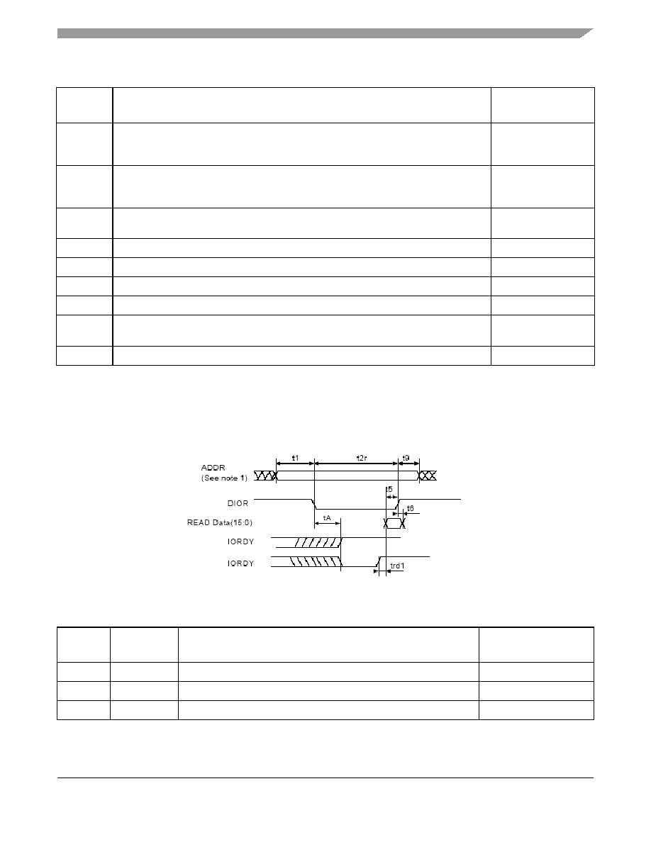
Electrical Characteristics
i.MX31/i.MX31L Advance Information, Rev. 1.4
Freescale Semiconductor
73
Preliminary
4.3.5.2
PIO Mode Timing
Figure 9
shows timing for PIO read, and
Table 24
lists the timing parameters for PIO read.
Figure 9. PIO Read Timing Diagram
tskew1
Max difference in propagation delay bus clock L-to-H to any of following signals
ata_cs0, ata_cs1, ata_da2, ata_da1, ata_da0, ata_dior, ata_diow, ata_dmack,
ata_data (write), ata_buffer_en
7 ns
tskew2
Max difference in buffer propagation delay for any of following signals
ata_cs0, ata_cs1, ata_da2, ata_da1, ata_da0, ata_dior, ata_diow, ata_dmack,
ata_data (write), ata_buffer_en
transceiver
tskew3
Max difference in buffer propagation delay for any of following signals ata_iordy, ata_data
(read)
transceiver
tbuf
Max buffer propagation delay
transceiver
tcable1
cable propagation delay for ata_data
cable
tcable2
cable propagation delay for control signals ata_dior, ata_diow, ata_iordy, ata_dmack
cable
tskew4
Max difference in cable propagation delay between ata_iordy and ata_data (read)
cable
tskew5
Max difference in cable propagation delay between (ata_dior, ata_diow, ata_dmack)
and ata_cs0, ata_cs1, ata_da2, ata_da1, ata_da0, ata_data(write)
cable
tskew6
Max difference in cable propagation delay without accounting for ground bounce
cable
1
Values provided where applicable.
Table 24. PIO Read Timing Parameters
ATA
Parameter
Parameter
from
Figure 9
Value
Controlling
Variable
t1
t1
t1 (min) = time_1 * T - (tskew1 + tskew2 + tskew5)
time_1
t2
t2r
t2 min) = time_2r * T - (tskew1 + tskew2 + tskew5)
time_2r
t9
t9
t9 (min) = time_9 * T - (tskew1 + tskew2 + tskew6)
time_3
Table 23. ATA Timing Parameters (continued)
Name
Description
Value/
Contributing Factor
1
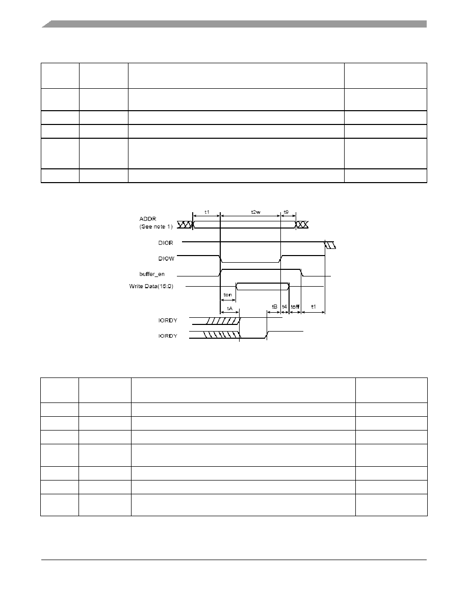
i.MX31/i.MX31L Advance Information, Rev. 1.4
74
Freescale Semiconductor
Preliminary
Electrical Characteristics
Figure 10
shows timing for PIO write, and
Table 25
lists the timing parameters for PIO write.
Figure 10. Multiword DMA (MDMA) Timing
t5
t5
t5 (min) = tco + tsu + tbuf + tbuf + tcable1 + tcable2
If not met, increase
time_2.
t6
t6
0
≠
tA
tA
tA (min) = (1.5 + time_ax) * T - (tco + tsui + tcable2 + tcable2 + 2*tbuf)
time_ax
trd
trd1
trd1 (max) = (-trd) + (tskew3 + tskew4)
trd1 (min) = (time_pio_rdx - 0.5)*T - (tsu + thi)
(time_pio_rdx - 0.5) * T > tsu + thi + tskew3 + tskew4
time_pio_rdx
t0
≠
t0 (min) = (time_1 + time_2 + time_9) * T
time_1, time_2r, time_9
Table 25. PIO Write Timing Parameters
ATA
Parameter
Parameter
from
Figure 10
Value
Controlling
Variable
t1
t1
t1 (min) = time_1 * T - (tskew1 + tskew2 + tskew5)
time_1
t2
t2w
t2 (min) = time_2w * T - (tskew1 + tskew2 + tskew5)
time_2w
t9
t9
t9 (min) = time_9 * T - (tskew1 + tskew2 + tskew6)
time_9
t3
≠
t3 (min) = (time_2w - time_on)* T - (tskew1 + tskew2 +tskew5)
If not met, increase
time_2w.
t4
t4
t4 (min) = time_4 * T - tskew1
time_4
tA
tA
tA = (1.5 + time_ax) * T - (tco + tsui + tcable2 + tcable2 + 2*tbuf)
time_ax
t0
≠
t0(min) = (time_1 + time_2 + time_9) * T
time_1, time_2r,
time_9
Table 24. PIO Read Timing Parameters (continued)
ATA
Parameter
Parameter
from
Figure 9
Value
Controlling
Variable
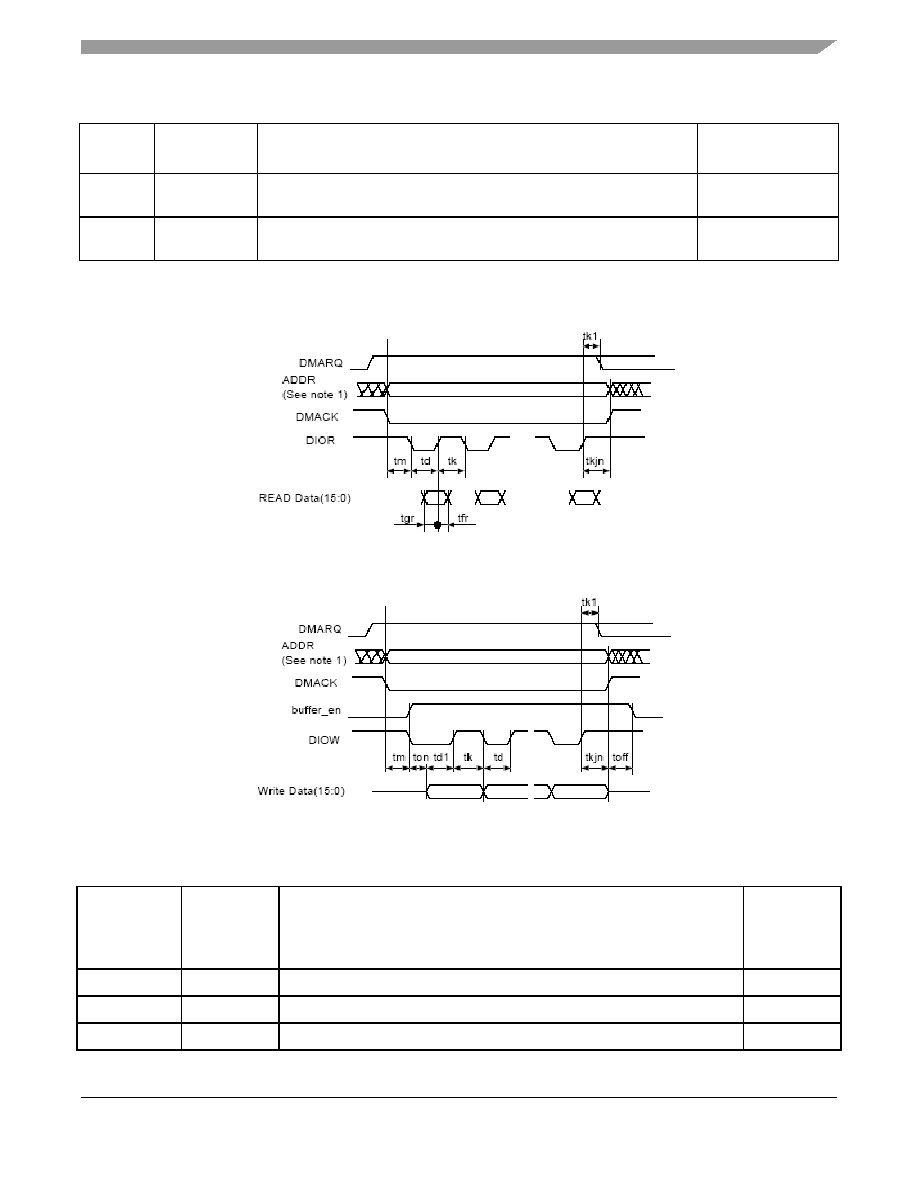
Electrical Characteristics
i.MX31/i.MX31L Advance Information, Rev. 1.4
Freescale Semiconductor
75
Preliminary
Figure 11
shows timing for MDMA read,
Figure 12
shows timing for MDMA write, and
Table 26
lists the
timing parameters for MDMA read and write.
Figure 11. MDMA Read Timing Diagram
Figure 12. MDMA Write Timing Diagram
≠
≠
Avoid bus contention when switching buffer on by making ton long
enough.
≠
≠
≠
Avoid bus contention when switching buffer off by making toff long
enough.
≠
Table 26. MDMA Read and Write Timing Parameters
ATA Parameter
Parameter
from
Figure 11
,
Figure 12
Value
Controlling
Variable
tm, ti
tm
tm (min) = ti (min) = time_m * T - (tskew1 + tskew2 + tskew5)
time_m
td
td, td1
td1.(min) = td (min) = time_d * T - (tskew1 + tskew2 + tskew6)
time_d
tk
tk
tk.(min) = time_k * T - (tskew1 + tskew2 + tskew6)
time_k
Table 25. PIO Write Timing Parameters (continued)
ATA
Parameter
Parameter
from
Figure 10
Value
Controlling
Variable
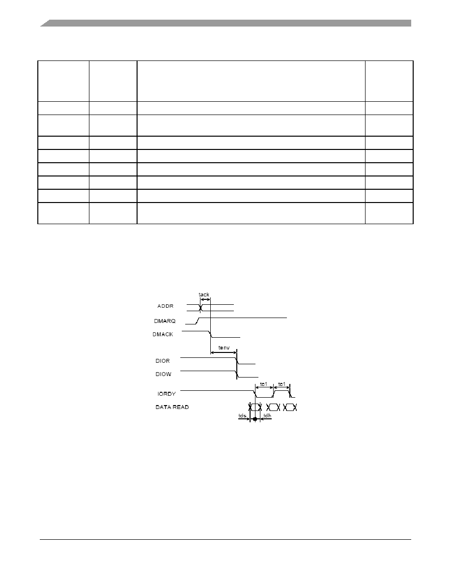
i.MX31/i.MX31L Advance Information, Rev. 1.4
76
Freescale Semiconductor
Preliminary
Electrical Characteristics
4.3.5.3
UDMA In Timing
Figure 13
shows timing when the UDMA in transfer starts,
Figure 14
shows timing when the UDMA in
host terminates transfer,
Figure 15
shows timing when the UDMA in device terminates transfer, and
Table 27
lists the timing parameters for UDMA in burst.
Figure 13. UDMA In Transfer Starts Timing Diagram
t0
≠
t0 (min) = (time_d + time_k) * T
time_d, time_k
tg(read)
tgr
tgr (min-read) = tco + tsu + tbuf + tbuf + tcable1 + tcable2
tgr.(min-drive) = td - te(drive)
time_d
tf(read)
tfr
tfr (min-drive) = 0
≠
tg(write)
≠
tg (min-write) = time_d * T - (tskew1 + tskew2 + tskew5)
time_d
tf(write)
≠
tf (min-write) = time_k * T - (tskew1 + tskew2 + tskew6)
time_k
tL
≠
tL (max) = (time_d + time_k-2)*T - (tsu + tco + 2*tbuf + 2*tcable2)
time_d, time_k
tn, tj
tkjn
tn= tj= tkjn = (max(time_k,. time_jn) * T - (tskew1 + tskew2 + tskew6)
time_jn
≠
ton
toff
ton = time_on * T - tskew1
toff = time_off * T - tskew1
≠
Table 26. MDMA Read and Write Timing Parameters (continued)
ATA Parameter
Parameter
from
Figure 11
,
Figure 12
Value
Controlling
Variable
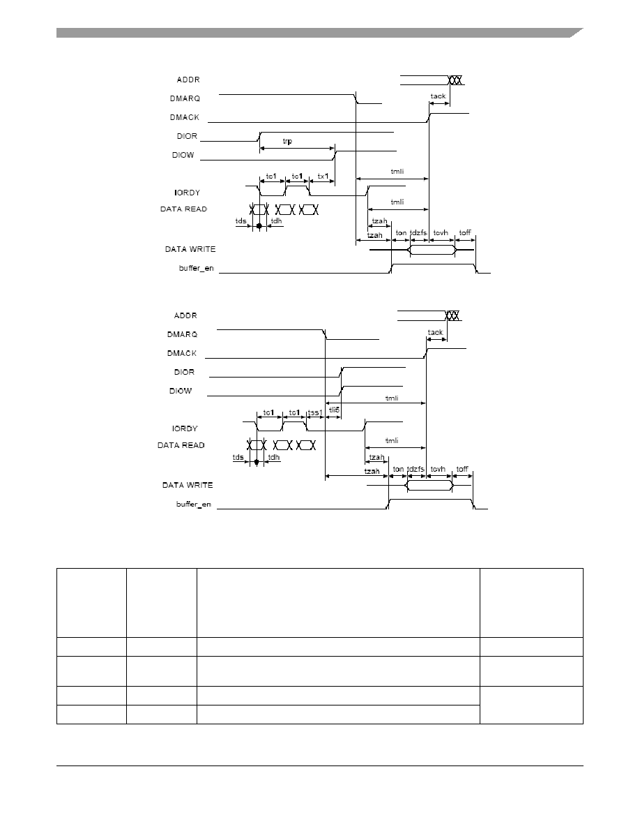
Electrical Characteristics
i.MX31/i.MX31L Advance Information, Rev. 1.4
Freescale Semiconductor
77
Preliminary
Figure 14. UDMA In Host Terminates Transfer Timing Diagram
Figure 15. UDMA In Device Terminates Transfer Timing Diagram
Table 27. UDMA In Burst Timing Parameters
ATA
Parameter
Parameter
from
Figure 13
,
Figure 14
,
Figure 15
Description
Controlling Variable
tack
tack
tack (min) = (time_ack * T) - (tskew1 + tskew2)
time_ack
tenv
tenv
tenv (min) = (time_env * T) - (tskew1 + tskew2)
tenv (max) = (time_env * T) + (tskew1 + tskew2)
time_env
tds
tds1
tds - (tskew3) - ti_ds > 0
tskew3, ti_ds, ti_dh
should be low enough
tdh
tdh1
tdh - (tskew3) -ti_dh > 0
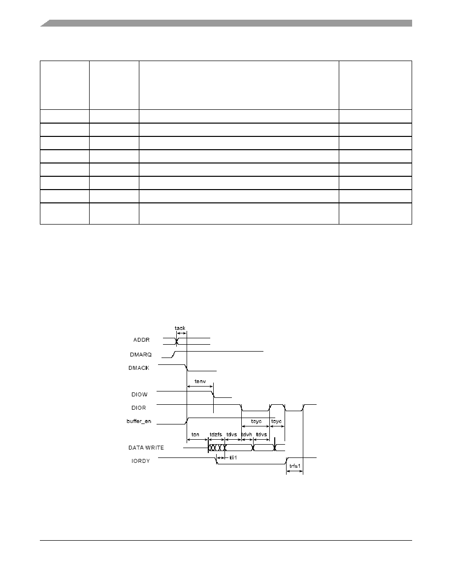
i.MX31/i.MX31L Advance Information, Rev. 1.4
78
Freescale Semiconductor
Preliminary
Electrical Characteristics
4.3.5.4 UDMA Out Timing
Figure 16
shows timing when the UDMA out transfer starts,
Figure 17
shows timing when the UDMA out
host terminates transfer,
Figure 18
shows timing when the UDMA out device terminates transfer, and
Table 28
lists the timing parameters for UDMA out burst.
Figure 16. UDMA Out Transfer Starts Timing Diagram
tcyc
tc1
(tcyc - tskew) > T
T big enough
trp
trp
trp (min) = time_rp * T - (tskew1 + tskew2 + tskew6)
time_rp
≠
tx1
1
(time_rp * T) - (tco + tsu + 3T + 2 *tbuf + 2*tcable2) > trfs (drive)
time_rp
tmli
tmli1
tmli1 (min) = (time_mlix + 0.4) * T
time_mlix
tzah
tzah
tzah (min) = (time_zah + 0.4) * T
time_zah
tdzfs
tdzfs
tdzfs = (time_dzfs * T) - (tskew1 + tskew2)
time_dzfs
tcvh
tcvh
tcvh = (time_cvh *T) - (tskew1 + tskew2)
time_cvh
≠
ton
toff
ton = time_on * T - tskew1
toff = time_off * T - tskew1
≠
1
There is a special timing requirement in the ATA host that requires the internal DIOW to go only high 3 clocks after the last
active edge on the DSTROBE signal. The equation given on this line tries to capture this constraint.
2. Make ton and toff big enough to avoid bus contention
Table 27. UDMA In Burst Timing Parameters (continued)
ATA
Parameter
Parameter
from
Figure 13
,
Figure 14
,
Figure 15
Description
Controlling Variable
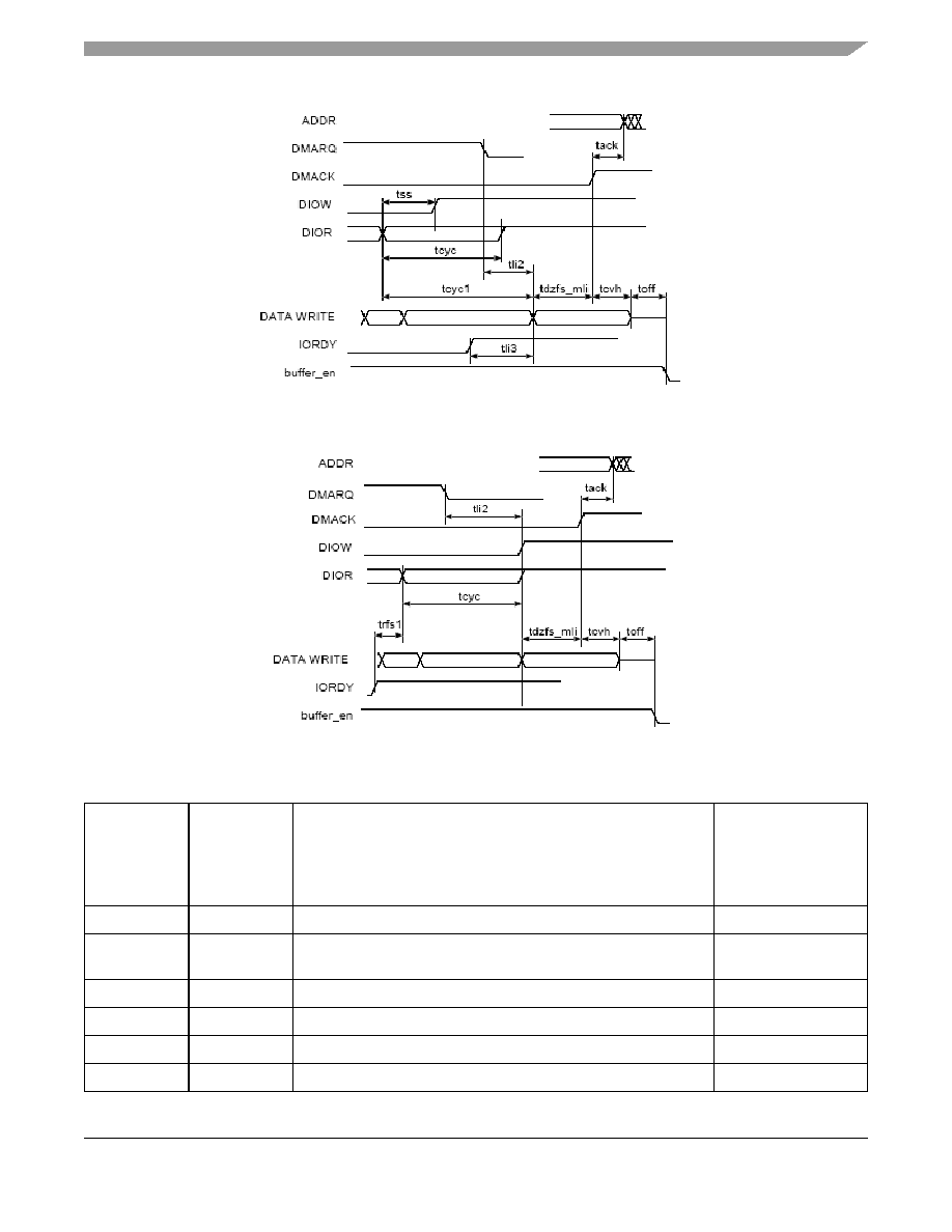
Electrical Characteristics
i.MX31/i.MX31L Advance Information, Rev. 1.4
Freescale Semiconductor
79
Preliminary
Figure 17. UDMA Out Host Terminates Transfer Timing Diagram
Figure 18. UDMA Out Device Terminates Transfer Timing Diagram
Table 28. UDMA Out Burst Timing Parameters
ATA
Parameter
Parameter
from
Figure 16
,
Figure 17
,
Figure 18
Value
Controlling
Variable
tack
tack
tack (min) = (time_ack * T) - (tskew1 + tskew2)
time_ack
tenv
tenv
tenv (min) = (time_env * T) - (tskew1 + tskew2)
tenv (max) = (time_env * T) + (tskew1 + tskew2)
time_env
tdvs
tdvs
tdvs = (time_dvs * T) - (tskew1 + tskew2)
time_dvs
tdvh
tdvh
tdvs = (time_dvh * T) - (tskew1 + tskew2)
time_dvh
tcyc
tcyc
tcyc = time_cyc * T - (tskew1 + tskew2)
time_cyc
t2cyc
≠
t2cyc = time_cyc * 2 * T
time_cyc
i.MX31/i.MX31L Advance Information, Rev. 1.4
80
Freescale Semiconductor
Preliminary
Electrical Characteristics
4.3.6
AUDMUX Electrical Specifications
The AUDMUX provides a programmable interconnect logic for voice, audio and data routing between
internal serial interfaces (SSI) and external serial interfaces (audio and voice codecs). The AC timing of
AUDMUX external pins is hence governed by the SSI module. Please refer to their respective electrical
specifications.
4.3.7
CSPI Electrical Specifications
This section describes the electrical information of the CSPI.
4.3.7.1
CSPI Timing
Figure 19
and
Figure 20
depict the master mode and slave mode timings of CSPI, and
Table 29
lists the
timing parameters.
trfs1
trfs
trfs = 1.6 * T + tsui + tco + tbuf + tbuf
≠
≠
tdzfs
tdzfs = time_dzfs * T - (tskew1)
time_dzfs
tss
tss
tss = time_ss * T - (tskew1 + tskew2)
time_ss
tmli
tdzfs_mli
tdzfs_mli =max (time_dzfs, time_mli) * T - (tskew1 + tskew2)
≠
tli
tli1
tli1 > 0
≠
tli
tli2
tli2 > 0
≠
tli
tli3
tli3 > 0
≠
tcvh
tcvh
tcvh = (time_cvh *T) - (tskew1 + tskew2)
time_cvh
≠
ton
toff
ton = time_on * T - tskew1
toff = time_off * T - tskew1
≠
Table 28. UDMA Out Burst Timing Parameters (continued)
ATA
Parameter
Parameter
from
Figure 16
,
Figure 17
,
Figure 18
Value
Controlling
Variable
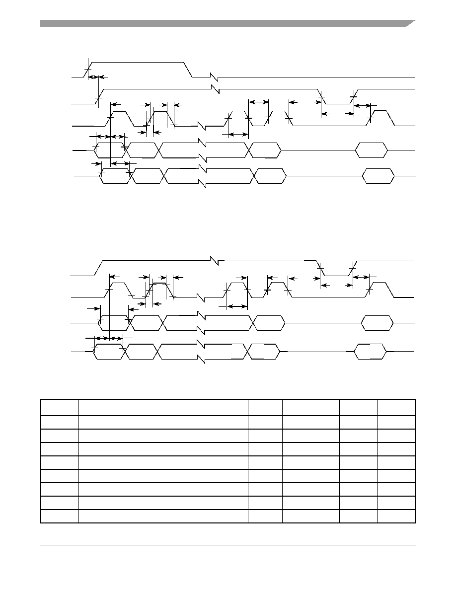
Electrical Characteristics
i.MX31/i.MX31L Advance Information, Rev. 1.4
Freescale Semiconductor
81
Preliminary
Figure 19. CSPI Master Mode Timing Diagram
NOTE
CSPI1_DRYN is connected to CSPI1_CS_1, CSPI2_DRYN is connected to
DAM2_T_CLK
Figure 20. CSPI Slave Mode Timing Diagram
Table 29. CSPI Interface Timing Parameters
ID
Parameter
Symbol
Min
Max
Units
CS1
CSPIx_CLK Cycle Time
t
clk
60
≠
ns
CS2
CSPIx_CLK High or Low Time
t
SW
30
≠
ns
CS3
CSPIx_CLK Rise or Fall
t
RISE/FALL
≠
7.6
ns
CS4
CSPIx_CS_x pulse width
t
CSLH
25
≠
ns
CS5
CSPIx_CS_x Lead Time (CS setup time)
t
SCS
25
≠
ns
CS6
CSPIx_CS_x Lag Time (CS hold time)
t
HCS
25
≠
ns
CS7
CSPIx_DO Setup Time
t
Smosi
5
≠
ns
CS8
CSPIx_DO Hold Time
t
Hmosi
5
≠
ns
CS1
CS7
CS8
CS2
CS2
CS4
CS6
CS5
CS9
CS10
CSPIx_CLK
CSPIx_CS_x
CSPIx_DO
CSPIx_DI
CSPIx_DRYN
CS11
CS3
CS3
CS7
CS8
CS2
CS2
CS4
CS6
CS9
CS10
CSPIx_CLK
CSPIx_CS_x
CSPIx_DI
CSPIx_DO
CS1
CS3
CS3
CS5
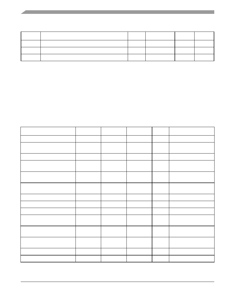
i.MX31/i.MX31L Advance Information, Rev. 1.4
82
Freescale Semiconductor
Preliminary
Electrical Characteristics
4.3.8
DPLL Electrical Specifications
The three PLL's of the MX31/MX31L (MCU, USB, and Serial PLL) are all based on same DPLL design.
The characteristics provided herein apply to all of them, except where noted explicitly. The PLL
characteristics are provided based on measurements done for both sources--external clock source (CKIH),
and FPM (Frequency Pre-Multiplier) source.
4.3.8.1
Electrical Specifications
Table 30
lists the DPLL specification.
CS9
CSPIx_DI Setup Time
t
Smiso
5
≠
ns
CS10
CSPIx_DI Hold Time
t
Hmiso
5
≠
ns
CS11
CSPIx_DRYN Setup Time
t
SDRY
5
≠
ns
Table 30. DPLL Specifications
Parameter
Min
Typ
Max
Unit
Comments
CKIH reference frequency
10
-
100
MHz
≠
CKIL referencer frequency (FPM
enable mode)
32; 32.768,
38.4
≠
MHz
≠
Predivision factor
1
≠
16
≠
PLL reference frequency range
after Predivider
10
≠
35
MHz
≠
Maximum allowed reference clock
phase noise.
10
≠
±
100
µs
≠
Frequency lock time
(FOL mode or non-integer MF)
≠
≠
398
µs
Cycles of divided reference
clock.
Phase lock time
≠
≠
100
µs
In addition to the frequency
PLL Power supply voltage
1.4
≠
1.6
V
≠
Single PLL current consumption
≠
≠
4.4
mA
≠
Maximum allowed PLL supply
voltage ripple
≠
≠
25
mV
F
modulation
< 50 kHz
Maximum allowed PLL supply
voltage ripple
≠
≠
20
mV
F
modulation
< 300 kHz
Maximum allowed PLL supply
voltage ripple
≠
≠
25
mV
F
modulation
< 300 kHz
PLL output clock phase jitter
≠
≠
5.2
ns
Measured on CKO pin
PLL output clock phase jitter
≠
≠
420
ns
Measured on CKO pin
Table 29. CSPI Interface Timing Parameters (continued)
ID
Parameter
Symbol
Min
Max
Units
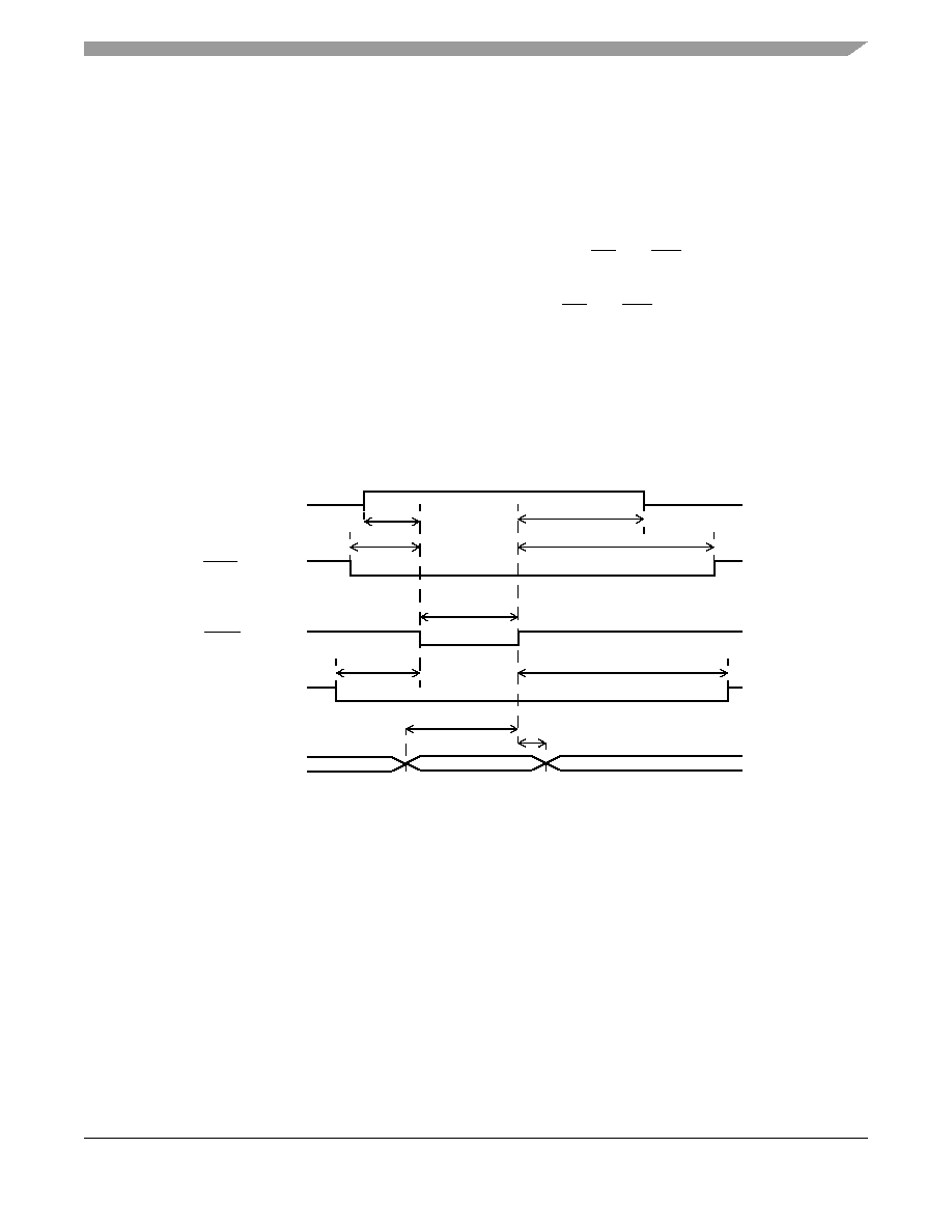
Electrical Characteristics
i.MX31/i.MX31L Advance Information, Rev. 1.4
Freescale Semiconductor
83
Preliminary
4.3.9
EMI Electrical Specifications
This section provides electrical parametrics and timings for EMI module.
4.3.9.1
NAND Flash Controller Interface (NFC)
There are two modes of operations for the NFC--default and ONE_CYCLE.
Normal NFC mode--using two flash clock cycles for one access of RE and WE. AC parameters
calculation for this mode assume the flash clock cycle frequency is 22.5 MHz (as an example).
One-Cycle NFC mode--using one flash cycle for one access of RE and WE. AC parameters calculation
for this mode assume the flash clock cycle frequency that is 33.5 MHz (as an example).
4.3.9.1.1
Normal NFC Mode (Default)
The flash clock maximum frequency goes up to 50 MHz.
Figure 21
,
Figure 22
,
Figure 23
, and
Figure 24
depict the relative timing requirements among different signals of the NFC at module level, for normal
mode, and
Table 31
lists the timing parameters.
Figure 21. Command Latch Cycle Timing DIagram
NFCLE
NFCE
NFWE
NFALE
NFIO[7:0]
Command
NF9
NF8
NF1
NF2
NF5
NF3
NF4
NF6
NF7
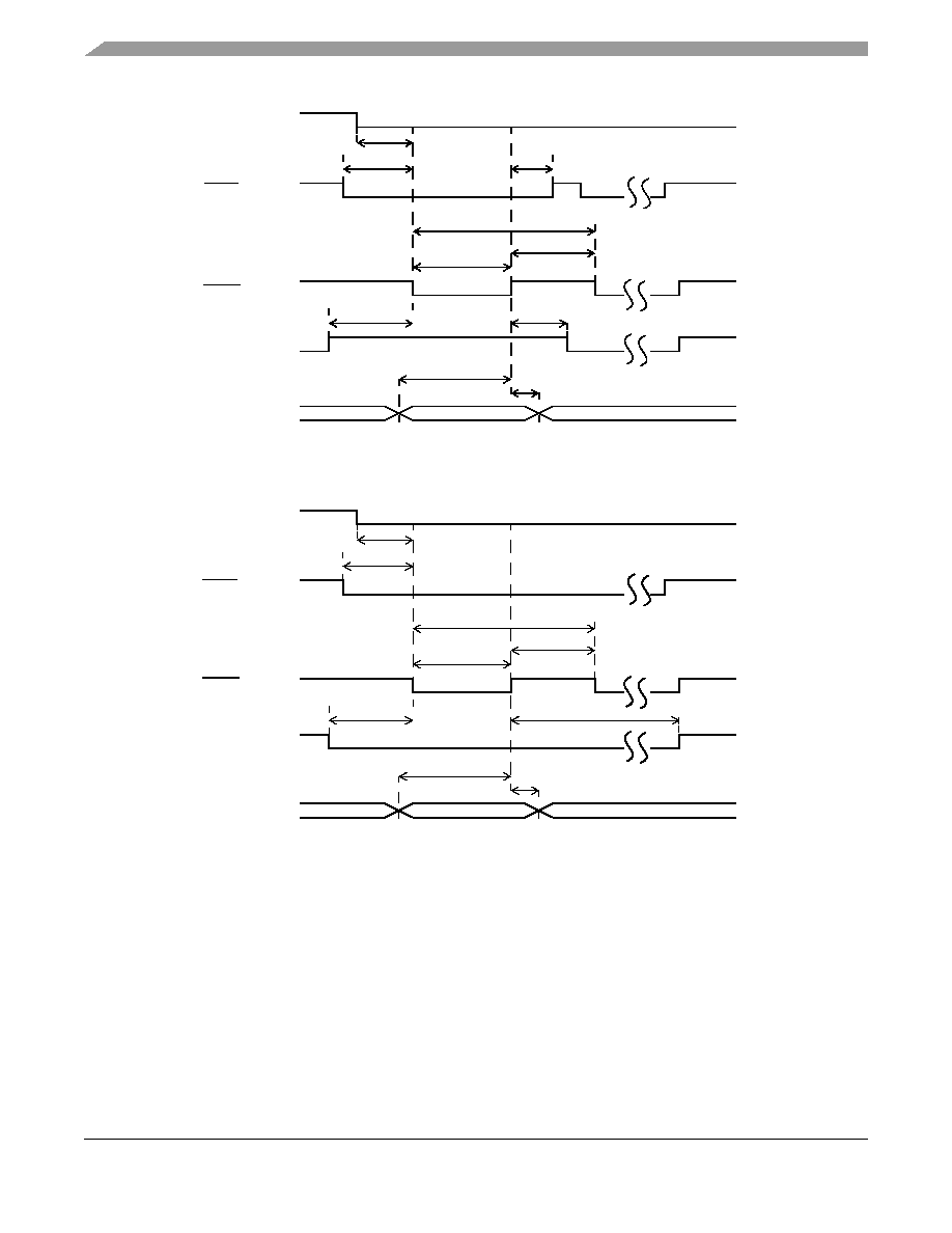
i.MX31/i.MX31L Advance Information, Rev. 1.4
84
Freescale Semiconductor
Preliminary
Electrical Characteristics
Figure 22. Address Latch Cycle Timing DIagram
Figure 23. Write Data Latch Cycle Timing DIagram
NFCLE
NFCE
NFWE
NFALE
NFIO[7:0]
Address
NF9
NF8
NF1
NF5
NF3
NF4
NF6
NF11
NF10
NF7
NFCLE
NFCE
NFWE
NFALE
NFIO[15:0]
Data to NF
NF9
NF8
NF1
NF5
NF3
NF6
NF11
NF10
NF7
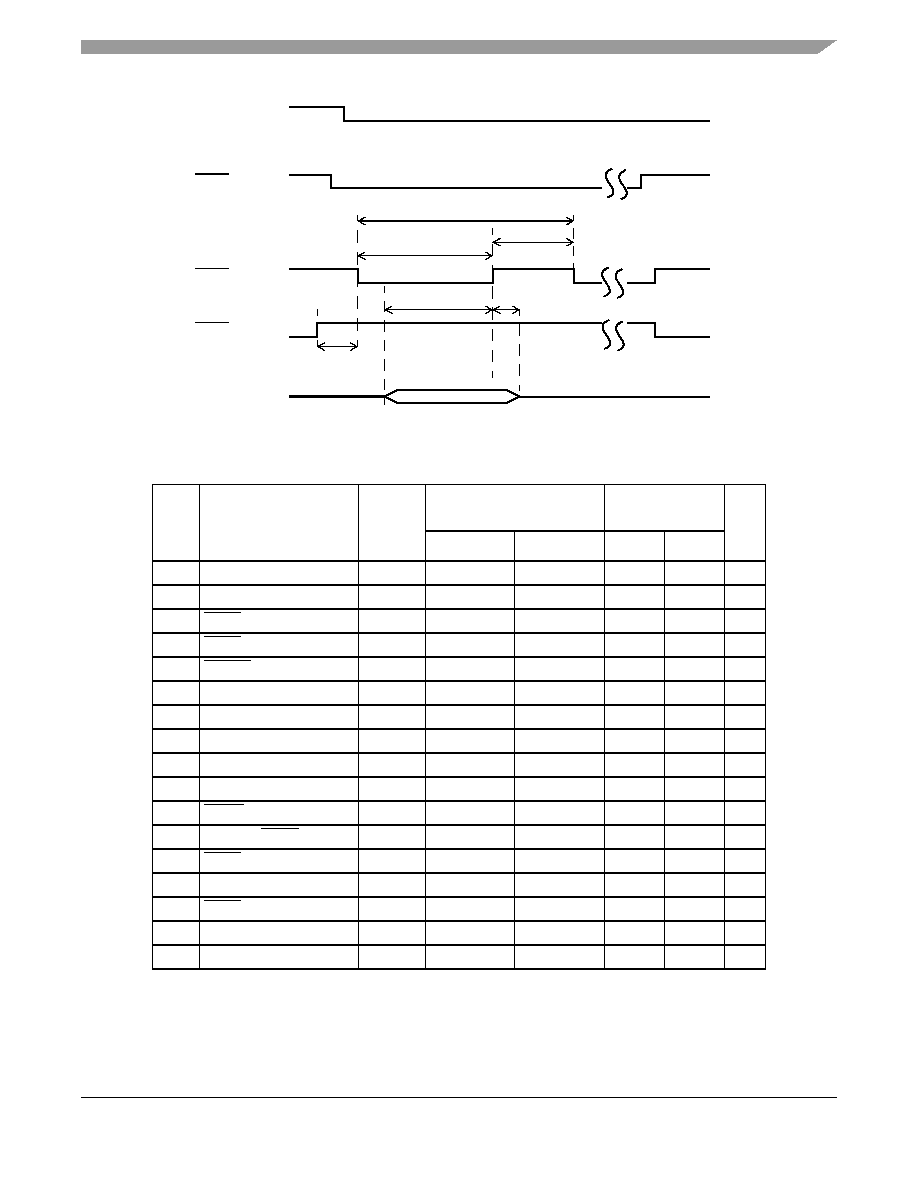
Electrical Characteristics
i.MX31/i.MX31L Advance Information, Rev. 1.4
Freescale Semiconductor
85
Preliminary
Figure 24. Read Data Latch Cycle Timing DIagram
NOTE
High is defined as 80% of signal value and low is defined as 20% of signal
value.
Table 31. NFC Target Timing Parameters
ID
Parameter
Symbol
Relationship to NFC clock
Period (T)
Unit
Min
Max
Min
Max
NF1
NFCLE Setup Time
tCLS
T
≠
45
≠
ns
NF2
NFCLE Hold Time
tCLH
T
≠
45
≠
ns
NF3
NFCE Setup Time
tCS
T
≠
90
≠
ns
NF4
NFCE Hold Time
tCH
T
≠
45
≠
ns
NF5
NF_WP Pulse Width
tWP
T
≠
45
≠
ns
NF6
NFALE Setup Time
tALS
T
≠
45
≠
ns
NF7
NFALE Hold Time
tALH
T
≠
45
≠
ns
NF8
Data Setup Time
tDS
T
≠
90
≠
ns
NF9
Data Hold Time
tDH
T
≠
45
≠
ns
NF10 Write Cycle Time
tWC
2T
≠
90
≠
ns
NF11 NFWE Hold Time
tWH
T
≠
45
≠
ns
NF12 Ready to NFRE Low
tRR
6T
≠
270
≠
ns
NF13 NFRE Pulse Width
tRP
1.5T
≠
67.5
≠
ns
NF14 READ Cycle Time
tRC
2T
≠
90
≠
ns
NF15 NFRE High Hold Time
tREH
0.5T
≠
22.5
≠
ns
NF16 Data Setup on READ
tDSR
≠
≠
15
≠
ns
NF17 Data Hold on READ
tDHR
≠
≠
5
≠
ns
NFCLE
NFCE
NFRE
NFRB
NFIO[15:0]
Data from NF
NF13
NF15
NF14
NF17
NF12
NF16
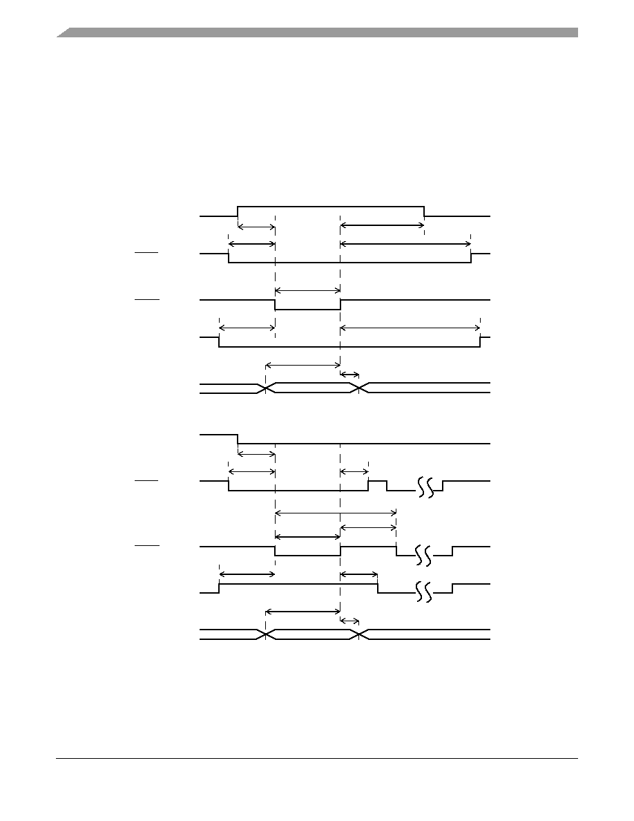
i.MX31/i.MX31L Advance Information, Rev. 1.4
86
Freescale Semiconductor
Preliminary
Electrical Characteristics
NOTE
Timing for HCLK is 133 MHz and internal LCLK (flash clock) is 22.5 MHz
(45 ns). All timings are listed according to this LCLK frequency (multiples
of LCLK phases) except NF16, which is not LCLK related.
4.3.9.1.2
One-Cycle NFC Mode
Figure 25
,
Figure 26
,
Figure 27
, and
Figure 28
depict the relative timing requirements among different
signals of the NFC at module level for one-cycle mode, and
Table 32
lists the timing parameters.
Figure 25. Command Latch Cycle Timing DIagram--One Flash Clock Cycle
Figure 26. Address Latch Cycle Timing DIagram--One Flash Clock Cycle
NFCLE
NFCE
NFWE
NFALE
NFIO[7:0]
command
NF9_one
NF8_one
NF1_one
NF2_one
NF5_one
NF3_one
NF4_one
NF6_one
NF7_one
NFCLE
NFCE
NFWE
NFALE
NFIO[7:0]
Address
NF9_one
NF8_one
NF1_one
NF5_one
NF3_one
NF4_one
NF6_one
NF11_one
NF10_one
NF7_one
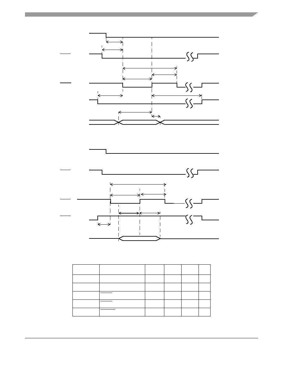
Electrical Characteristics
i.MX31/i.MX31L Advance Information, Rev. 1.4
Freescale Semiconductor
87
Preliminary
Figure 27. Write Data Latch Cycle Timing DIagram--One Flash Clock Cycle
Figure 28. Read Data Latch Cycle Timing DIagram--One Flash Clock Cycle
Table 32. NFC Target Timing Parameters--One Flash Clock Cycle
ID
Parameter
Symbol
Min
Max
Unit
NF1_one
NFCLE Setup Time
tCLS
30
≠
ns
NF2_one
NFCLE Hold Time
tCLH
30
≠
ns
NF3_one
NFCE Setup Time
tCS
60
≠
ns
NF4_one
NFCE Hold Time
tCH
45
≠
ns
NF5_one
NF_WP Pulse Width
tWP
15
≠
ns
NFCLE
NFCE
NFWE
NFALE
NFIO[15:0]
Data to NF
NF9_one
NF8_one
NF1_one
NF5_one
NF3_one
NF6_one
NF11_one
NF10_one
NF7_one
NFCLE
NFCE
NFRE
NFRB
NFIO[15:0]
Data from NF
NF13_one
NF15_one
NF14_one
NF12_one
NF16_one
NF17_one
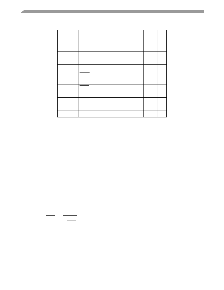
i.MX31/i.MX31L Advance Information, Rev. 1.4
88
Freescale Semiconductor
Preliminary
Electrical Characteristics
NOTE
High is defined as 80% of signal value and low is defined as 20% of signal
value.
NOTE
Timing for HCLK is 133 MHz and internal LCLK (flash clock) is 33.25 MHz
(30 ns). All timings are listed according to this LCLK frequency.
4.3.9.2
Wireless External Interface Module (WEIM)
All WEIM output control signals may be asserted and deasserted by internal clock related to BCLK rising
edge or falling edge according to corresponding assertion/negation control fields. Address always begins
related to BCLK falling edge but may be ended both on rising and falling edge in muxed mode according
to control register configuration. Output data begins related to BCLK rising edge except in muxed mode
where both rising and falling edge may be used according to control register configuration. Input data,
ECB and DTACK all captured according to BCLK rising edge time.
Figure 29
depicts the timing of the
WEIM module, and
Table 33
lists the timing parameters.
NOTE
ECB and DTACK signals mentioned in this section can be connected to one
input pad--ECB, although the WEIM design has those two signals as
individual inputs. In this case, this PAD will be connected to the 2 WEIM
inputs.
NF6_one
NFALE Setup Time
tALS
30
≠
ns
NF7_one
NFALE Hold Time
tALH
30
≠
ns
NF8_one
Data Setup Time
tDS
15
≠
ns
NF9_one
Data Hold Time
tDH
15
≠
ns
NF10_one
Write Cycle Time
tWC
30
≠
ns
NF11_one
NFWE Hold Time
tWH
15
≠
ns
NF12_one
Ready to NFRE Low
tRR
180
≠
ns
NF13_one
NFRE Pulse Width
tRP
15
≠
ns
NF14_one
READ Cycle Time
tRC
30
≠
ns
NF15_one
NFRE High Hold Time
tREH
15
≠
ns
NF16_one
Data Setup on READ
tDSR
12
≠
ns
NF17_one
Data Hold on READ
tDHR
5
≠
ns
Table 32. NFC Target Timing Parameters--One Flash Clock Cycle (continued)
ID
Parameter
Symbol
Min
Max
Unit
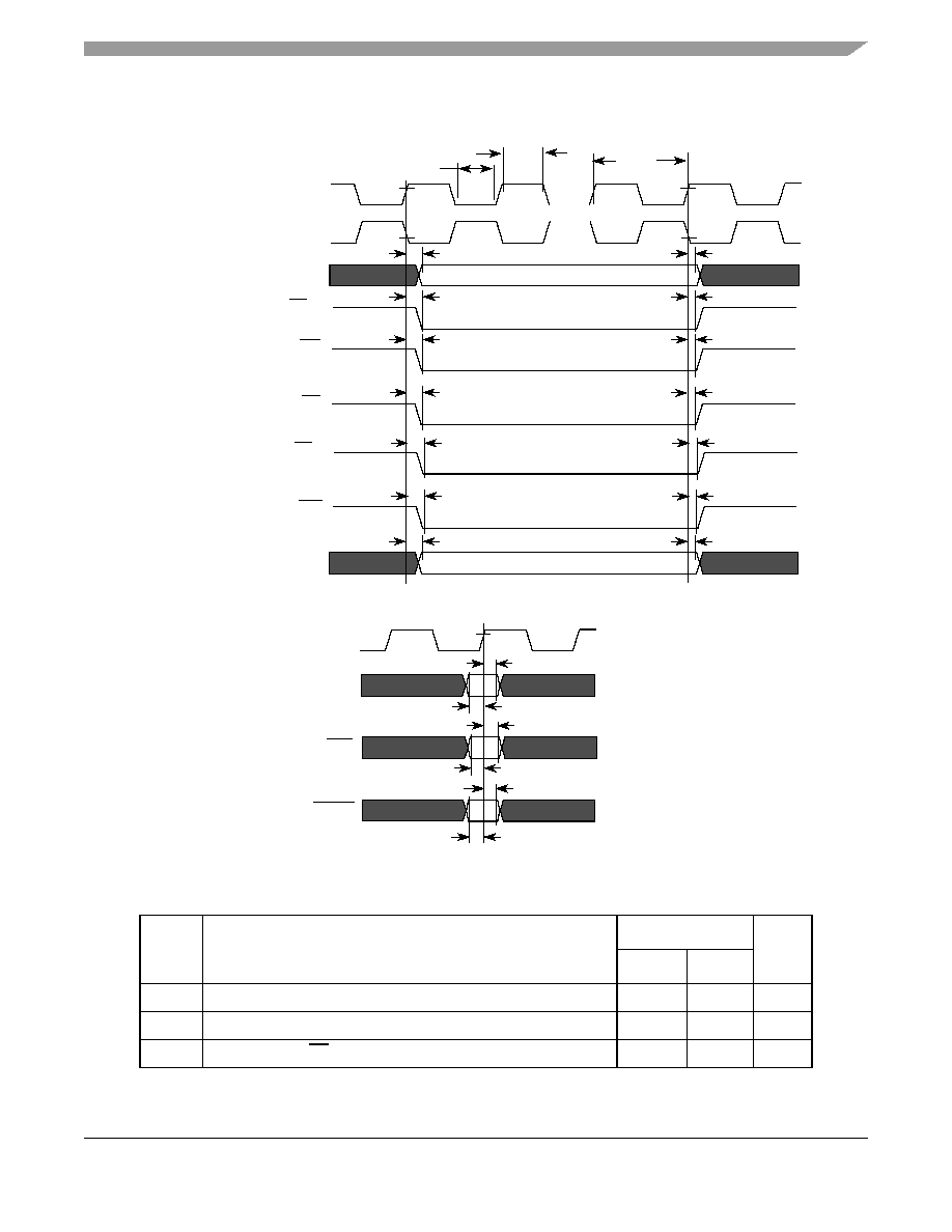
Electrical Characteristics
i.MX31/i.MX31L Advance Information, Rev. 1.4
Freescale Semiconductor
89
Preliminary
,
Figure 29. WEIM Bus Timing Diagram
Table 33. WEIM Bus Timing Parameters
ID
Parameter
1.8 V
Unit
Min
Max
WE1
Clock fall to address valid
≠2
7
ns
WE2
Clock rise/fall to address invalid
≠2
7
ns
WE3
Clock rise/fall to CS[x] valid
≠3
3
ns
WE1
WE2
WE3
WE4
WE5 WE6
WE7
WE8
WE9
WE10
WE11
WE12
WE13 WE14
WE16
WE15
WE18
WE17
WE20
WE19
WE21
WE22
WE23
BCLK (for rising edge timing)
BCLK (for falling edge timing)
Address
CS[x]
RW
OE
EB[x]
LBA
Output Data
BCLK (for rising edge timing)
Input Data
WEIM Outputs Timing
WEIM Inputs timing
ECB
DTACK
...
...
i.MX31/i.MX31L Advance Information, Rev. 1.4
90
Freescale Semiconductor
Preliminary
Electrical Characteristics
NOTE
High is defined as 80% of signal value and low is defined as 20% of signal value.
WE4
Clock rise/fall to CS[x] invalid
≠3
3
ns
WE5
Clock rise/fall to RW Valid
≠3
3
ns
WE6
Clock rise/fall to RW Invalid
≠3
3
ns
WE7
Clock rise/fall to OE Valid
≠3
3
ns
WE8
Clock rise/fall to OE Invalid
≠3
3
ns
WE9
Clock rise/fall to EB[x] Valid
≠3
3
ns
WE10
Clock rise/fall to EB[x] Invalid
≠3
3
ns
WE11
Clock rise/fall to LBA Valid
≠3
3
ns
WE12
Clock rise/fall to LBA Invalid
≠3
3
ns
WE13
Clock rise/fall to Output Data Valid
≠3.5
10
ns
WE14
Clock rise to Output Data Invalid
≠3.5
10
ns
WE15
Input Data Valid to Clock rise, FCE=0
≠2
10
ns
WE16
Cloc/k rise to Input Data Invalid, FCE=0
≠7
0
ns
WE15
Input Data Valid to Clock rise, FCE=1
≠2
10
ns
WE16
Clock rise to Input Data Invalid, FCE=1
≠7
0
ns
WE17
ECB setup time, FCE=0
≠2
10
ns
WE18
ECB hold time, FCE=0
≠7
0
ns
WE17
ECB setup time, FCE=1
≠2
10
ns
WE18
ECB hold time, FCE=1
≠7
0
ns
WE19
DTACK setup time
1
≠
≠
ns
WE20
DTACK hold time
0
4
ns
WE20
DTACK hold time (Level sensitive mode, EW=1
implies wsc < 111111)
6
12
ns
WE21
BCLK High Level Width
2, 3
≠
Tcycle/
2-3
ns
WE22
BCLK Low Level Width
2, 3
≠
Tcycle/
2-3
ns
WE23
BCLK Cycle time
2
≠
1
Not required.
2
BCLK parameters are being measured from the 50% VDD.
3
The actual cycle time is derived from the AHB bus clock frequency.
Table 33. WEIM Bus Timing Parameters (continued)
ID
Parameter
1.8 V
Unit
Min
Max
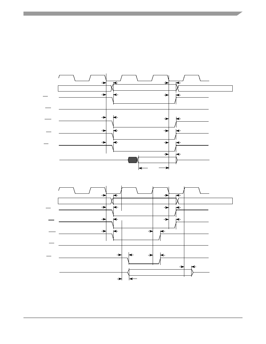
Electrical Characteristics
i.MX31/i.MX31L Advance Information, Rev. 1.4
Freescale Semiconductor
91
Preliminary
NOTE
Test conditions: pad voltage, 1.75 V-1.95 V; pad capacitance, 25 pF.
Recommended drive strength for all controls, address, and BCLK is Max drive.
Figure 30
,
Figure 31
,
Figure 32
,
Figure 33
,
Figure 34
, and
Figure 35
depict some examples of
basic WEIM accesses to external memory devices with the timing parameters mentioned in
Table 33
for specific control parameter settings.
Figure 30. Asynchronous Memory Timing Diagram for Read Access--WSC=1
Figure 31. Asynchronous Memory Timing Diagram for Write Access--
WSC=1, EBWA=1, EBWN=1, LBN=1
Last Valid Address
V1
V1
BCLK
ADDR
DATA
RW
LBA
OE
EB[y]
CS[x]
Next Address
WE1
WE2
WE3
WE4
WE7
WE8
WE10
WE9
WE11
WE12
WE15
WE16
Last Valid Address
V1
V1
BCLK
ADDR
DATA
RW
LBA
OE
EB[y]
CS[x]
Next Address
WE1
WE2
WE3
WE4
WE5
WE6
WE9
WE10
WE11
WE12
WE13
WE14
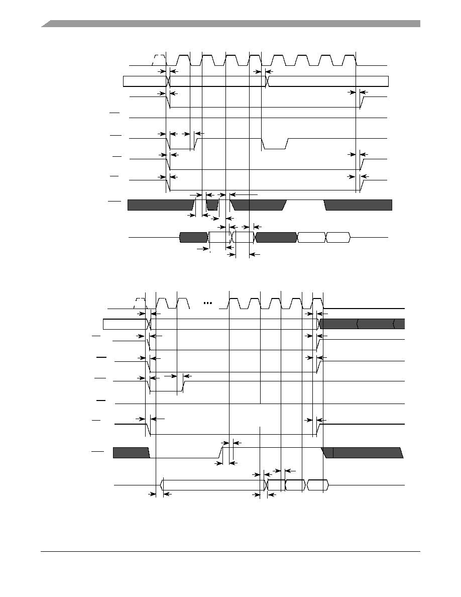
i.MX31/i.MX31L Advance Information, Rev. 1.4
92
Freescale Semiconductor
Preliminary
Electrical Characteristics
Figure 32. Synchronous Memory Timing Diagram for Two Non-Sequential Read Accesses--
WSC=2, SYNC=1, DOL=0
Figure 33. Synchronous Memory TIming Diagram for Burst Write Access--
BCS=1, WSC=4, SYNC=1, DOL=0, PSR=1
Last Valid Addr
Address V1
Address V2
V1
V1+2
V2
V2+2
BCLK
ADDR
ECB
DATA
Halfword
Halfword
CS[x]
RW
LBA
OE
EB[y]
Halfword
Halfword
WE1
WE2
WE4
WE7
WE8
WE9
WE10
WE11
WE12
WE15
WE15
WE16
WE16
WE17
WE17
WE18
WE18
WE3
Last Valid Addr
BCLK
ADDR
DATA
CS[x]
RW
LBA
OE
EB[y]
ECB
Address V1
V1
V1+4
V1+12
V1+8
WE9
WE1
WE2
WE3
WE4
WE5
WE6
WE10
WE11
WE13
WE13
WE14
WE14
WE17
WE18
WE12
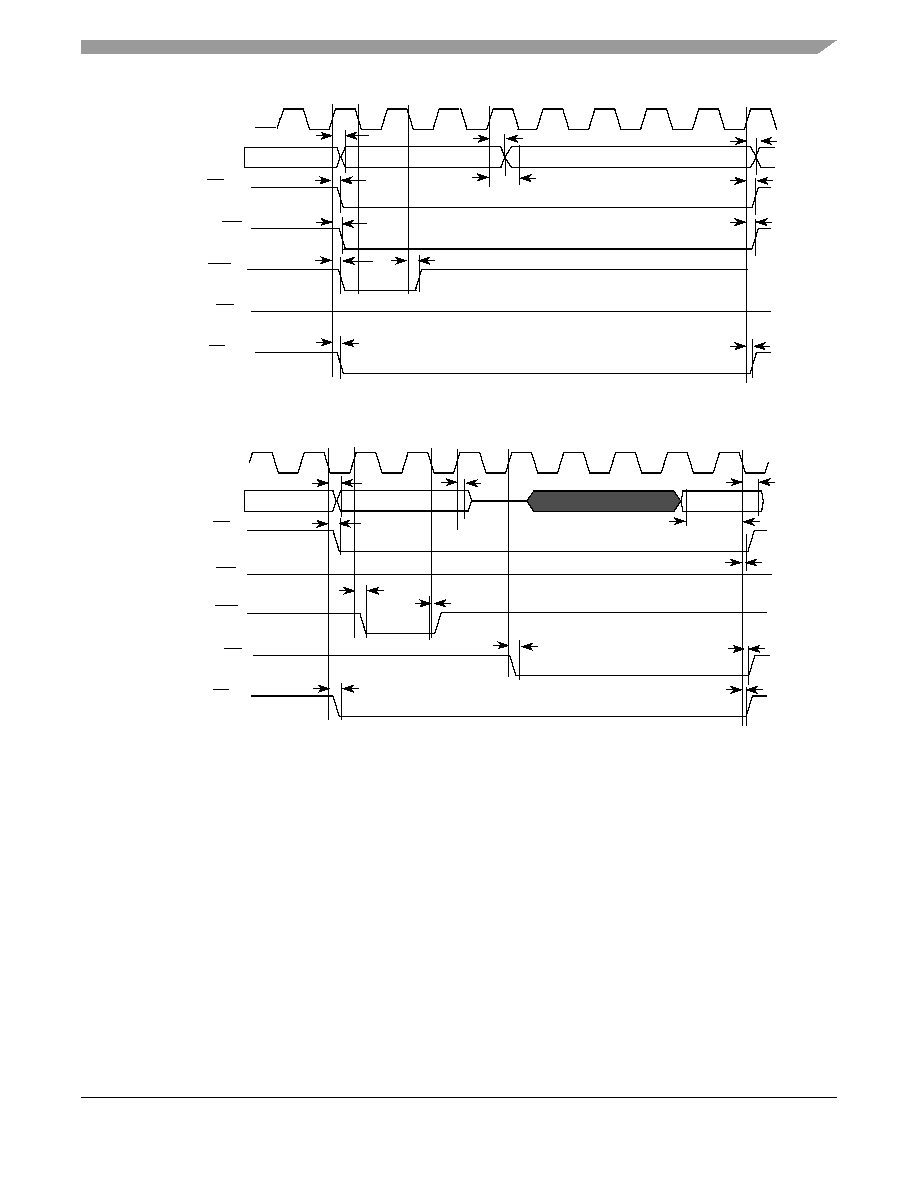
Electrical Characteristics
i.MX31/i.MX31L Advance Information, Rev. 1.4
Freescale Semiconductor
93
Preliminary
Figure 34. Muxed A/D Mode Timing Diagram for Asynchronous Write Access--
WSC=7, LBA=1, LBN=1, LAH=1
Figure 35. Muxed A/D Mode Timing Diagram for Asynchronous Read Access--
WSC=7, LBA=1, LBN=1, LAH=1, OEA=7
4.3.9.3
SDRAM (DDR and SDR) Memory Controller
Figure 36
,
Figure 37
,
Figure 38
,
Figure 39
,
Figure 40
, and
Figure 41
depict the timings pertaining to the
SDRAMC module, which interfaces Mobile DDR or SDR SDRAM.
Table 34
,
Table 35
,
Table 36
,
Table 37
,
Table 38
, and
Table 39
list the timing parameters.
Write
BCLK
ADDR/
RW
LBA
OE
EB[y]
CS[x]
Address V1
Write Data
Last Valid Addr
M_DATA
WE1
WE2
WE3
WE4
WE6
WE5
WE9
WE10
WE11
WE12
WE13
WE14
BCLK
ADDR/
RW
LBA
OE
EB[y]
CS[x]
Address V1
Read Data
Last Valid Addr
M_DATA
WE2
WE3
WE4
WE11
WE12
WE7
WE8
WE9
WE10
WE15
WE16
WE1
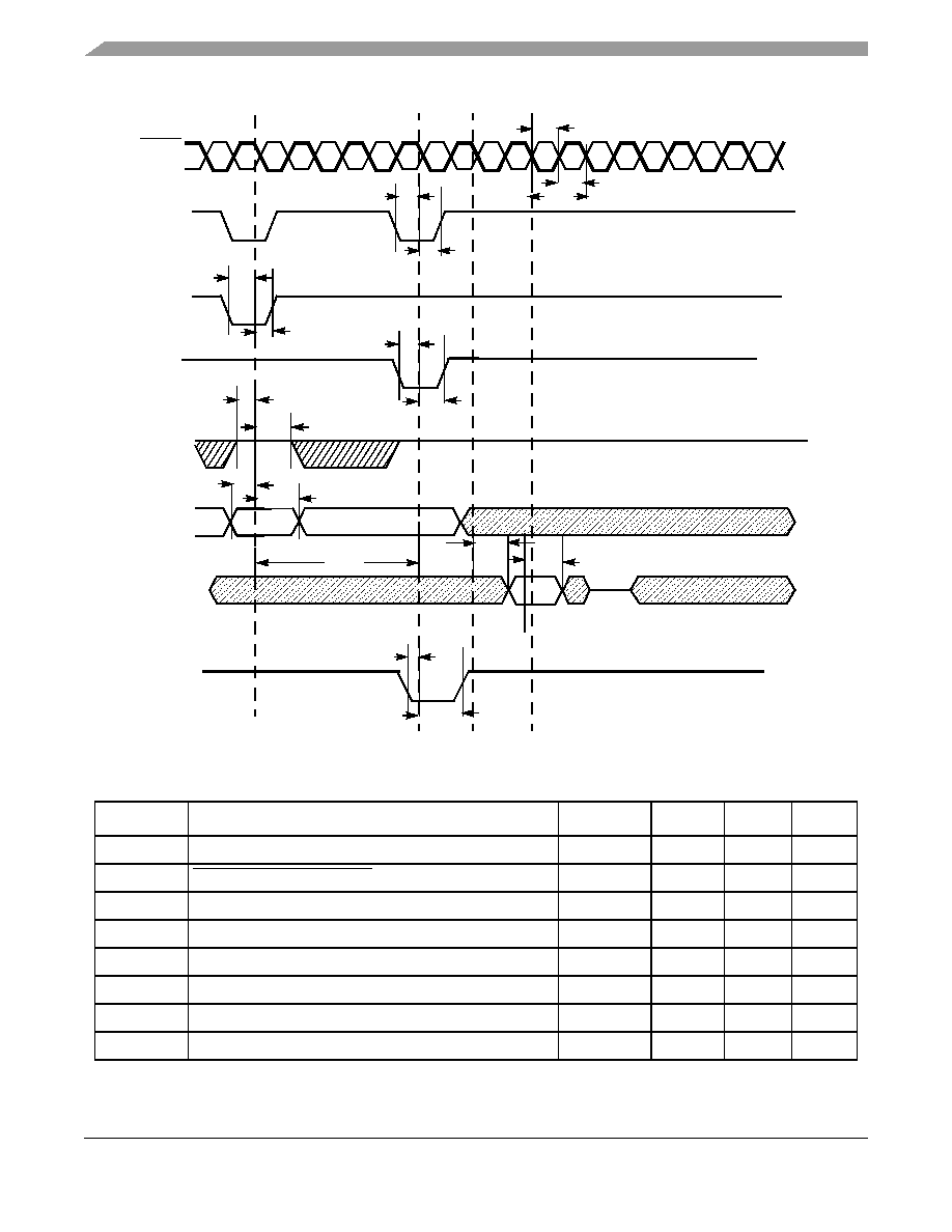
i.MX31/i.MX31L Advance Information, Rev. 1.4
94
Freescale Semiconductor
Preliminary
Electrical Characteristics
Figure 36. SDRAM Read Cycle Timing Diagram
Table 34. DDR/SDR SDRAM Read Cycle Timing Parameters
ID
Parameter
Symbol
Min
Max
Unit
SD1
SDRAM clock high-level width
tCH
3.4
4.1
ns
SD2
SDRAM clock low-level width
tCL
3.4
4.1
ns
SD3
SDRAM clock cycle time
tCK
7.5
≠
ns
SD4
CS, RAS, CAS, WE, DQM, CKE setup time
tCMS
2.0
≠
ns
SD5
CS, RAS, CAS, WE, DQM, CKE hold time
tCMH
1.8
≠
ns
SD6
Address output delay time
tAS
2.0
≠
ns
SD7
Address output hold time
tAH
1.8
≠
ns
SD8
SDRAM access time
tAC
≠
6.47
ns
SDCLK
WE
ADDR
DQ
DQM
ROW/BA
COL/BA
Data
CS
CAS
RAS
Note: CKE is high during the read/write cycle.
SD4
SD1
SD3
SD2
SD4
SD4
SD4
SD4
SD5
SD5
SD5
SD5
SD5
SD6
SD7
SD10
SD8
SD9
SDCLK

Electrical Characteristics
i.MX31/i.MX31L Advance Information, Rev. 1.4
Freescale Semiconductor
95
Preliminary
NOTE
SDR SDRAM CLK parameters are being measured from the 50%
point≠that is, high is defined as 50% of signal value and low is defined as
50% of signal value. SD1 + SD2 does not exceed 7.5 ns for 133 MHz.
NOTE
The timing parameters similar to the ones used in the regular SDRAM data
sheet. All output signals are driven by the ESDCTL at the negative edge of
SDCLK and the parameters are measured at maximum memory frequency.
SD9
Data out hold time
1
tOH
1.5
≠
ns
SD10
Active to read/write command period
tRC
10
≠
clock
1
Timing parameters are relevant only to SDR SDRAM. For the specific DDR SDRAM data related timing parameters, see
Table 38
and
Table 39
.
Table 34. DDR/SDR SDRAM Read Cycle Timing Parameters (continued)
ID
Parameter
Symbol
Min
Max
Unit
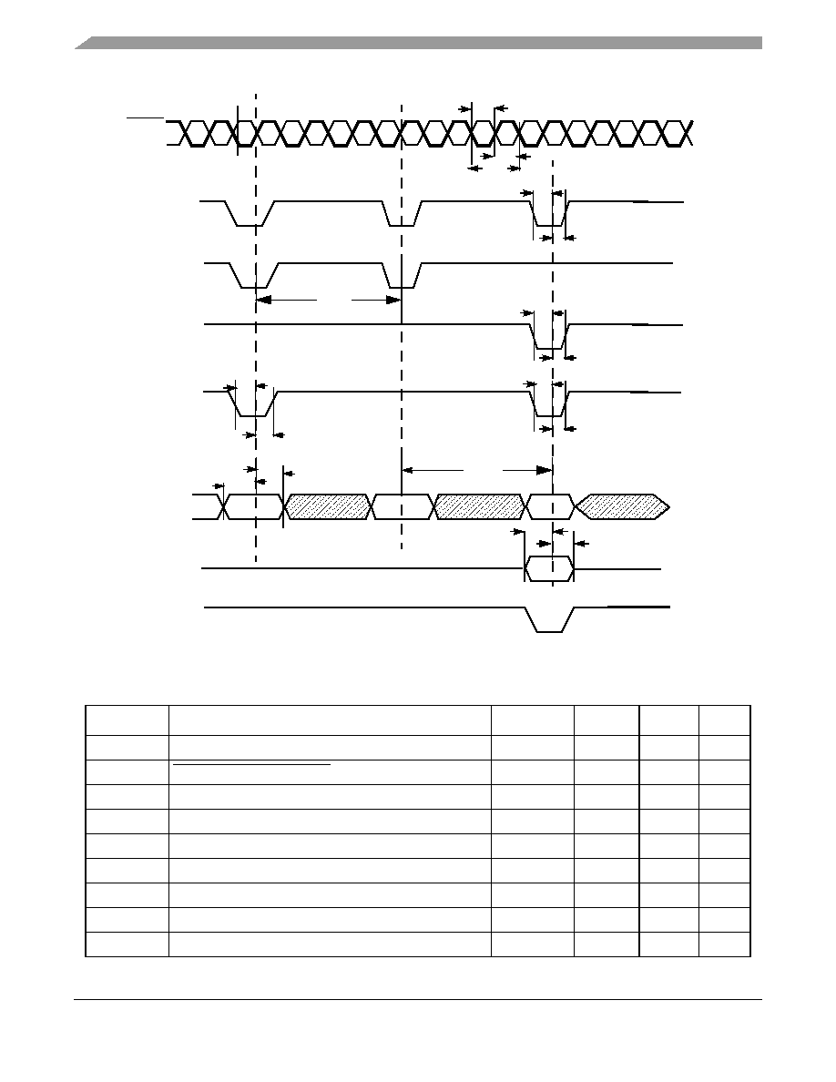
i.MX31/i.MX31L Advance Information, Rev. 1.4
96
Freescale Semiconductor
Preliminary
Electrical Characteristics
Figure 37. SDR SDRAM Write Cycle Timing Diagram
Table 35. SDR SDRAM Write Timing Parameters
ID
Parameter
Symbol
Min
Max
Unit
SD1
SDRAM clock high-level width
tCH
3.4
4.1
ns
SD2
SDRAM clock low-level width
tCL
3.4
4.1
ns
SD3
SDRAM clock cycle time
tCK
7.5
≠
ns
SD4
CS, RAS, CAS, WE, DQM, CKE setup time
tCMS
2.0
≠
ns
SD5
CS, RAS, CAS, WE, DQM, CKE hold time
tCMH
1.8
≠
ns
SD6
Address setup time
tAS
2.0
≠
ns
SD7
Address hold time
tAH
1.8
≠
ns
SD11
Precharge cycle period
1
tRP
1
4
clock
SD12
Active to read/write command delay
1
tRCD
1
8
clock
CS
CAS
WE
RAS
ADDR
DQ
DQM
BA
ROW / BA
COL/BA
DATA
SD4
SD4
SD4
SD4
SD5
SD5
SD5
SD5
SD7
SD6
SD12
SD13
SD14
SD11
SDCLK
SD1
SD3
SD2
SDCLK
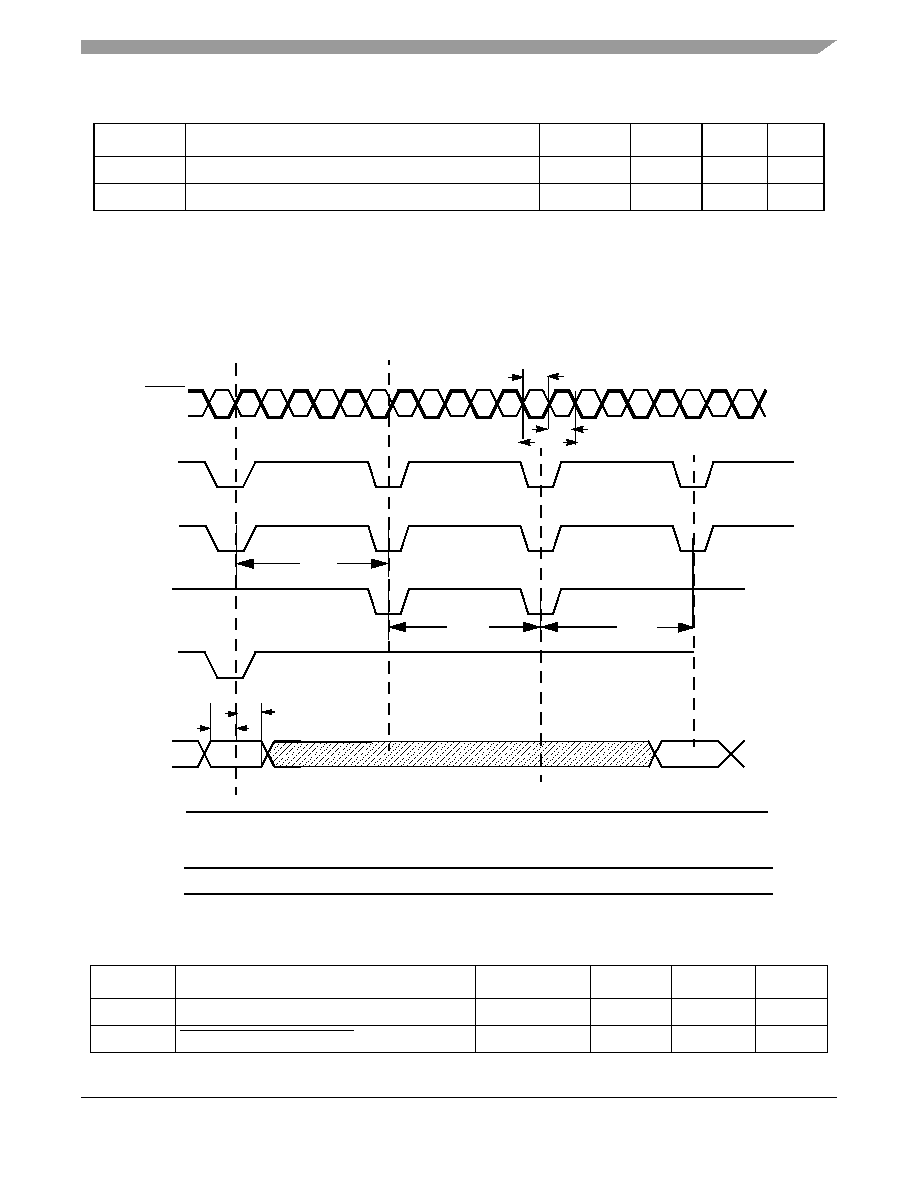
Electrical Characteristics
i.MX31/i.MX31L Advance Information, Rev. 1.4
Freescale Semiconductor
97
Preliminary
NOTE
SDR SDRAM CLK parameters are being measured from the 50%
point--that is, high is defined as 50% of signal value and low is defined as
50% of signal value.
Figure 38. SDRAM Refresh Timing Diagram
SD13
Data setup time
tDS
2.0
≠
ns
SD14
Data hold time
tDH
1.3
≠
ns
1
SD11 and SD12 are determined by SDRAM controller register settings.
Table 36. SDRAM Refresh Timing Parameters
ID
Parameter
Symbol
Min
Max
Unit
SD1
SDRAM clock high-level width
tCH
3.4
4.1
ns
SD2
SDRAM clock low-level width tCL
3.4
4.1
ns
Table 35. SDR SDRAM Write Timing Parameters (continued)
ID
Parameter
Symbol
Min
Max
Unit
CS
CAS
WE
RAS
ADDR
DQ
DQM
BA
ROW/BA
SD6
SD7
SD11
SD10
SD10
SDCLK
SD1
SD2
SDCLK
SD3
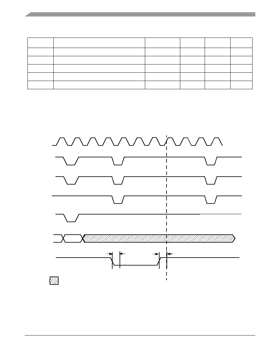
i.MX31/i.MX31L Advance Information, Rev. 1.4
98
Freescale Semiconductor
Preliminary
Electrical Characteristics
NOTE
SDR SDRAM CLK parameters are being measured from the 50%
point--that is, high is defined as 50% of signal value and low is defined as
50% of signal value.
Figure 39. SDRAM Self-Refresh Cycle Timing Diagram
NOTE
The clock will continue to run unless both CKEs are low. Then the clock will
be stopped in low state.
SD3
SDRAM clock cycle time
tCK
7.5
≠
ns
SD6
Address setup time
tAS
1.8
≠
ns
SD7
Address hold time
tAH
1.8
≠
ns
SD10
Precharge cycle period
1
tRP
1
4
clock
SD11
Auto precharge command period
1
tRC
2
20
clock
1
SD10 and SD11 are determined by SDRAM controller register settings.
Table 36. SDRAM Refresh Timing Parameters (continued)
ID
Parameter
Symbol
Min
Max
Unit
SDCLK
CS
CAS
RAS
ADDR
BA
WE
CKE
Don't care
SD16
SD16
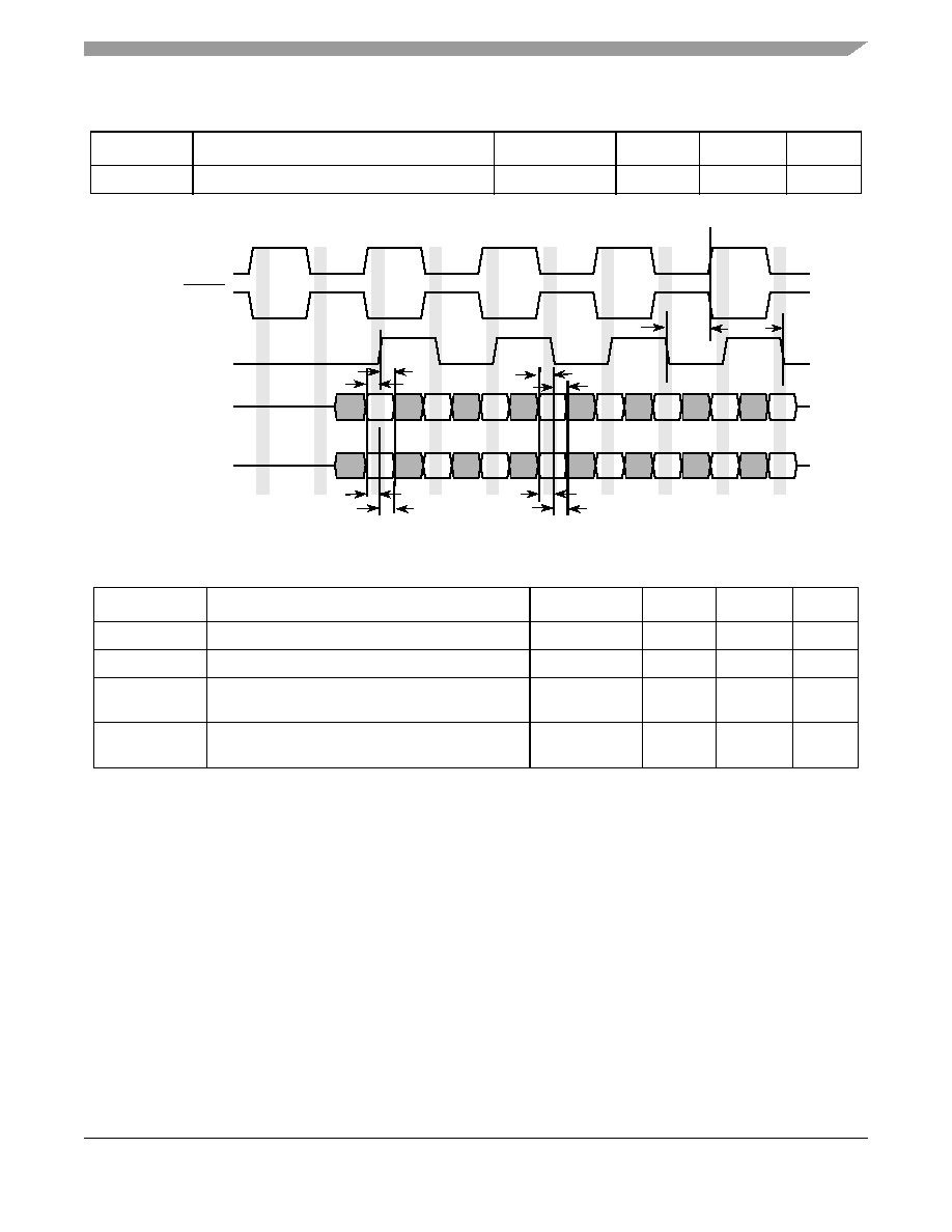
Electrical Characteristics
i.MX31/i.MX31L Advance Information, Rev. 1.4
Freescale Semiconductor
99
Preliminary
Figure 40. Mobile DDR SDRAM Write Cycle Timing Diagram
NOTE
SDRAM CLK and DQS related parameters are being measured from the
50% point--that is, high is defined as 50% of signal value and low is defined
as 50% of signal value.
Table 37. SDRAM Self-Refresh Cycle Timing Parameters
ID
Parameter
Symbol
Min
Max
Unit
SD16
CKE output delay time
tCKS
1.8
≠
ns
Table 38. Mobile DDR SDRAM Write Cycle Timing Parameters
ID
Parameter
Symbol
Min
Max
Unit
SD17
DQ & DQM setup time to DQS
tDS
1.2
≠
ns
SD18
DQ & DQM hold time to DQS
tDH
1.2
≠
ns
SD19
Write cycle DQS falling edge to SDCLK output
delay time.
tDSS
1.8
≠
ns
SD20
Write cycle DQS falling edge to SDCLK output hold
time.
tDSH
1.8
≠
ns
SDCLK
SDCLK
DQS (output)
DQ (output)
DQM (output)
Data
Data
Data
Data
Data
Data
Data
Data
DM
DM
DM
DM
DM
DM
DM
DM
SD17
SD17
SD17
SD17
SD18
SD18
SD18
SD18
SD19
SD20
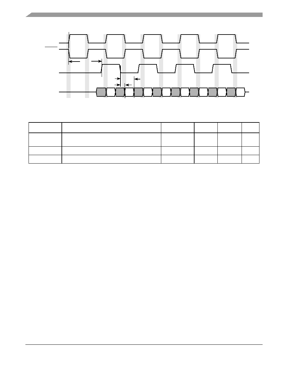
i.MX31/i.MX31L Advance Information, Rev. 1.4
100
Freescale Semiconductor
Preliminary
Electrical Characteristics
Figure 41. Mobile DDR SDRAM DQ versus DQS and SDCLK Read Cycle Timing Diagram
NOTE
SDRAM CLK and DQS related parameters are being measured from the
50% point--that is, high is defined as 50% of signal value and low is defined
as 50% of signal value.
4.3.10
ETM Electrical Specifications
ETM is an ARM protocol. There are no inherent restrictions on operating frequency, other than ASIC pad
technology and TPA limitations. ASIC designers must provide a TRACECLK as symmetrical as possible,
and with set-up and hold times as large as possible. TPA designers must conversely be able to support a
TRACECLK as asymmetrical as possible, and require set up and hold times as short as possible. The
timing specifications in this section are given as a guide for a TPA that supports TRACECLK frequencies
up to around 100 MHz.
NOTE
Actual processor clock frequencies vary according to application
requirements and the silicon process technologies used. The maximum
operating clock frequencies attained by ARM devices increases over time as
a result.
If a designer adheres to the timing described here, he or she can use any ARM-approved TPA.
Figure 42
depicts the TRACECLK timings of ETM, and
Table 40
lists the timing parameters.
Table 39. Mobile DDR SDRAM Read Cycle Timing Parameters
ID
Parameter
Symbol
Min
Max
Unit
SD21
DQS - DQ Skew (defines the Data valid window in
read cycles related to DQS).
tDQSQ
≠
.85
ns
SD22
DQS DQ HOLD time from DQS
tQH
2.3
≠
ns
SD23
DQS output access time from SDCLK posedge
tDQSCK
≠
6.7
ns
SDCLK
SDCLK
DQS (input)
DQ (input)
Data
Data
Data
Data
Data
Data
Data
Data
SD23
SD21
SD22
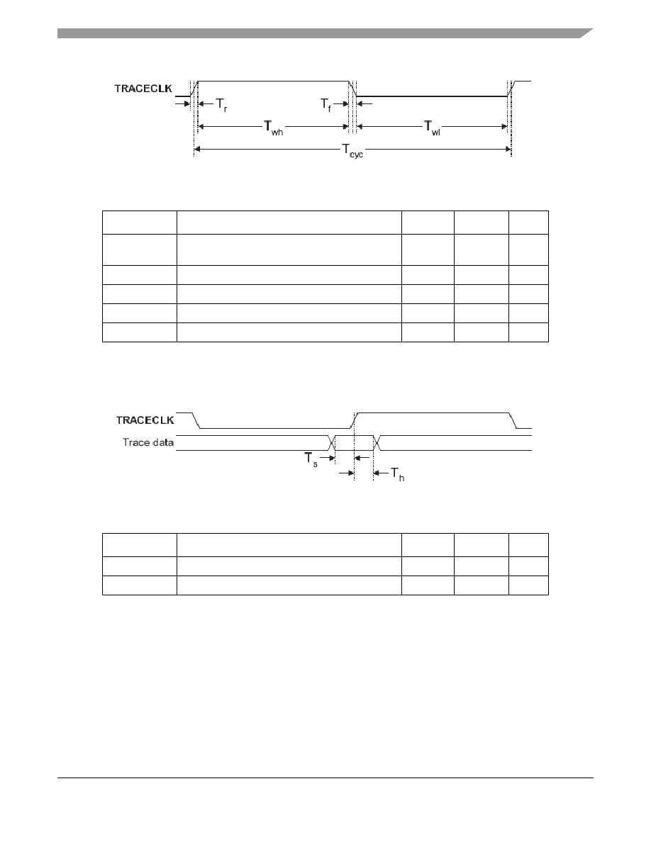
Electrical Characteristics
i.MX31/i.MX31L Advance Information, Rev. 1.4
Freescale Semiconductor
101
Preliminary
Figure 42. ETM TRACECLK Timing Diagram
Figure 43
depicts the setup and hold requirements of the trace data pins with respect to TRACECLK, and
Table 41
lists the timing parameters.
Figure 43. Trace Data Timing Diagram
4.3.10.1
Half-Rate Clocking Mode
When half-rate clocking is used, the trace data signals are sampled by the TPA on both the rising and falling
edges of TRACECLK, where TRACECLK is half the frequency of the clock shown in
Figure 43
.
4.3.11
FIR Electrical Specifications
FIR implements asynchronous infrared protocols (FIR, MIR) that are defined by IrDA
Æ
(Infrared Data
Association). Refer to http://www.IrDA.org for details on FIR and MIR protocols.
Table 40. ETM TRACECLK Timing Parameters
ID
Parameter
Min
Max
Unit
T
cyc
Clock period
Frequency
dependent
≠
ns
T
wl
Low pulse width
2
≠
ns
T
wh
High pulse width
2
≠
ns
T
r
Clock and data rise time
≠
3
ns
T
f
Clock and data fall time
≠
3
ns
Table 41. ETM Trace Data Timing Parameters
ID
Parameter
Min
Max
Unit
T
s
Data setup
2
≠
ns
T
h
Data hold
1
≠
ns
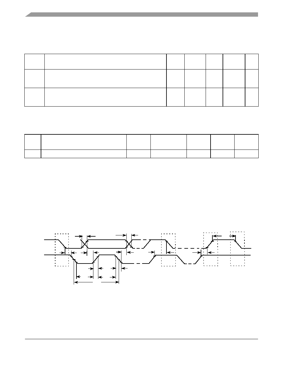
i.MX31/i.MX31L Advance Information, Rev. 1.4
102
Freescale Semiconductor
Preliminary
Electrical Characteristics
4.3.12
Fusebox Electrical Specifications
4.3.13
I2C Electrical Specifications
This section describes the electrical information of the I2C Module.
4.3.13.1
I2C Module Timing
Figure 44
depicts the timing of I2C module.
Table 44
lists the I2C module timing parameters where the
I/O supply is 2.7 V. 1
Figure 44. I2C Bus Timing Diagram
Table 42. Fusebox Supply Current Parameters
Ref.
Num
Description
Symbol Minimum Typical Maximum Units
1
eFuse Program Current.
1
Current to program one eFuse bit
efuse_pgm = 3.0V
1
The current I
program
is during program time (t
program
).
I
program
≠
35
60
mA
2
eFuse Read Current
2
Current to read an 8-bit eFuse word
vdd_fusebox = 1.875V
2
The current I
read
is present for approximately 50nS of the read access to the 8 bit word
I
read
≠
5
8
mA
Table 43. Fusebox Timing Characteristics
Ref.
Num
Description
Symbol
Minimum
Typical
Maximum
Units
1
Program time for eFuse
1
1
The program length is defined by the value defined in the epm_pgm_length[2:0] bits of the IIM module. The value to program
is based on a 32 kHz clock source (4 * 1/32 kHz = 125 µs)
t
program
125
≠
≠
µs
IC10
IC11
IC9
IC2
IC8
IC4
IC7
IC3
IC6
IC10
IC5
IC11
START
STOP
START
START
I2DAT
I2CLK
IC1
Electrical Characteristics
i.MX31/i.MX31L Advance Information, Rev. 1.4
Freescale Semiconductor
103
Preliminary
4.3.14
IPU--Sensor Interfaces
4.3.14.1
Supported Sensors
Table 45
lists the supported camera sensors by vendor and model.
Table 44. I2C Module Timing Parameters--I2C Pin I/O Supply=2.7 V
ID
Parameter
Standard Mode
Fast Mode
Unit
Min
Max
Min
Max
IC1
I2CLK cycle time
10
≠
2.5
≠
µs
IC2
Hold time (repeated) START condition
4.0
≠
0.6
≠
µs
IC3
Set-up time for STOP condition
4.0
≠
0.6
≠
µs
IC4
Data hold time
0
1
1
A device must internally provide a hold time of at least 300 ns for I2DAT signal in order to bridge the undefined region of the
falling edge of I2CLK.
3.45
2
2
The maximum hold time has to be met only if the device does not stretch the LOW period (ID IC6) of the I2CLK signal.
0
1
0.9
2
µs
IC5
HIGH Period of I2CLK Clock
4.0
≠
0.6
≠
µs
IC6
LOW Period of the I2CLK Clock
4.7
≠
1.3
≠
µs
IC7
Set-up time for a repeated START condition
4.7
≠
0.6
≠
µs
IC8
Data set-up time
250
≠
100
3
3
A Fast-mode I2C-bus device can be used in a standard-mode I2C-bus system, but the requirement of set-up time (ID IC7) of
250 ns must then be met. This will automatically be the case if the device does not stretch the LOW period of the I2CLK signal.
If such a device does stretch the LOW period of the I2CLK signal, it must output the next data bit to the I2DAT line max_rise_time
(ID No IC10) + data_setup_time (ID No IC8) = 1000 + 250 = 1250 ns (according to the Standard-mode I2C-bus specification)
before the I2CLK line is released.
≠
ns
IC9
Bus free time between a STOP and START condition
4.7
≠
1.3
≠
µs
IC10
Rise time of both I2DAT and I2CLK signals
≠
1000
20+0.1C
b
4
4
C
b
= total capacitance of one bus line in pF.
300
ns
IC11
Fall time of both I2DAT and I2CLK signals
≠
300
20+0.1C
b
4
300
ns
IC12
Capacitive load for each bus line (C
b
)
≠
400
≠
400
pF
Table 45. Supported Camera Sensors
Vendor
Model
Conexant
CX11646, CX20490, CX20450
Agilant
HDCP-2010, ADCS-1021, ADCS-1021
Toshiba
TC90A70
ICMedia
ICM202A, ICM102
iMagic
IM8801
Transchip
TC5600, TC5600J, TC5640, TC5700, TC6000
i.MX31/i.MX31L Advance Information, Rev. 1.4
104
Freescale Semiconductor
Preliminary
Electrical Characteristics
4.3.14.2
Functional Description
There are three timing modes supported by the IPU.
4.3.14.2.1
Pseudo BT.656 Video Mode
Smart camera sensors, which include imaging processing, usually support video mode transfer. They use
an embedded timing syntax to replace the SENSB_VSYNC and SENSB_HSYNC signals. The timing
syntax is defined by the BT.656 standard.
This operation mode follows the recommendations of ITU BT.656 specifications. The only control signal
used is SENSB_PIX_CLK. Start-of-frame and active-line signals are embedded in the data stream. An
active line starts with a SAV code and ends with a EAV code. In some cases, digital blanking is inserted in
between EAV and SAV code. The CSI decodes and filters out the timing-coding from the data stream, thus
recovering SENSB_VSYNC and SENSB_HSYNC signals for internal use.
4.3.14.2.2
Gated Clock Mode
The SENSB_VSYNC, SENSB_HSYNC, and SENSB_PIX_CLK signals are used in this mode. See
Figure 45
.
Fujitsu
MB86S02A
Micron
MI-SOC-0133
Matsushita
MN39980
STMicro
W6411, W6500, W6501, W6600, W6552, STV0974
OmniVision
OV7620, OV6630
Sharp
LZ0P3714 (CCD)
Motorola
MC30300 (Python), SCM20014, SCM20114, SCM22114, SCM20027
National Semiconductor
LM9618
Table 45. Supported Camera Sensors (continued)
Vendor
Model
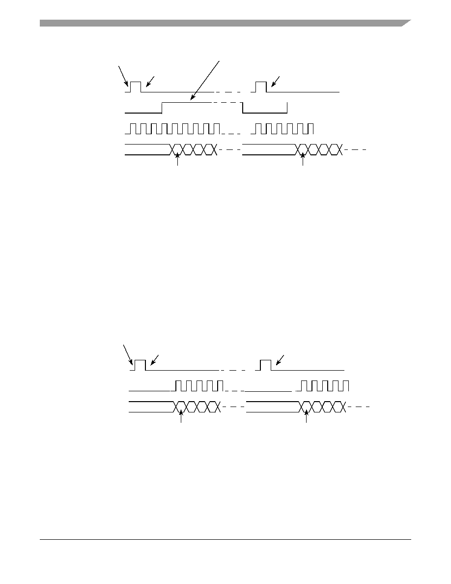
Electrical Characteristics
i.MX31/i.MX31L Advance Information, Rev. 1.4
Freescale Semiconductor
105
Preliminary
Figure 45. Gated Clock Mode Timing Diagram
A frame starts with a rising edge on SENSB_VSYNC (all the timings correspond to straight polarity of the
corresponding signals). Then SENSB_HSYNC goes to high and hold for the entire line. Pixel clock is valid
as long as SENSB_HSYNC is high. Data is latched at the rising edge of the valid pixel clocks.
SENSB_HSYNC goes to low at the end of line. Pixel clocks then become invalid and the CSI stops
receiving data from the stream. For next line the SENSB_HSYNC timing repeats. For next frame the
SENSB_VSYNC timing repeats.
4.3.14.2.3
Non-Gated Clock Mode
The timing is the same as the gated-clock mode (described in
Section 4.3.14.2.2, "Gated Clock Mode
"
on
page 104
), except for the SENSB_HSYNC signal, which is not used. See
Figure 46
. All incoming pixel
clocks are valid and will cause data to be latched into the input FIFO. The SENSB_PIX_CLK signal is
inactive (states low) until valid data is going to be transmitted over the bus.
Figure 46. Non-Gated Clock Mode Timing Diagram
The timing described in
Figure 46
is that of a Motorola sensor. Some other sensors may have a slightly
different timing. The CSI can be programmed to support rising/falling-edge triggered SENSB_VSYNC;
active-high/low SENSB_HSYNC; and rising/falling-edge triggered SENSB_PIX_CLK.
SENSB_VSYNC
SENSB_HSYNC
SENSB_PIX_CLK
SENSB_DATA[9:0]
invalid
1st byte
n+1th frame
invalid
1st byte
nth frame
Active Line
Start of Frame
SENSB_VSYNC
SENSB_PIX_CLK
SENSB_DATA[7:0]
invalid
1st byte
n+1th frame
invalid
1st byte
nth frame
Start of Frame
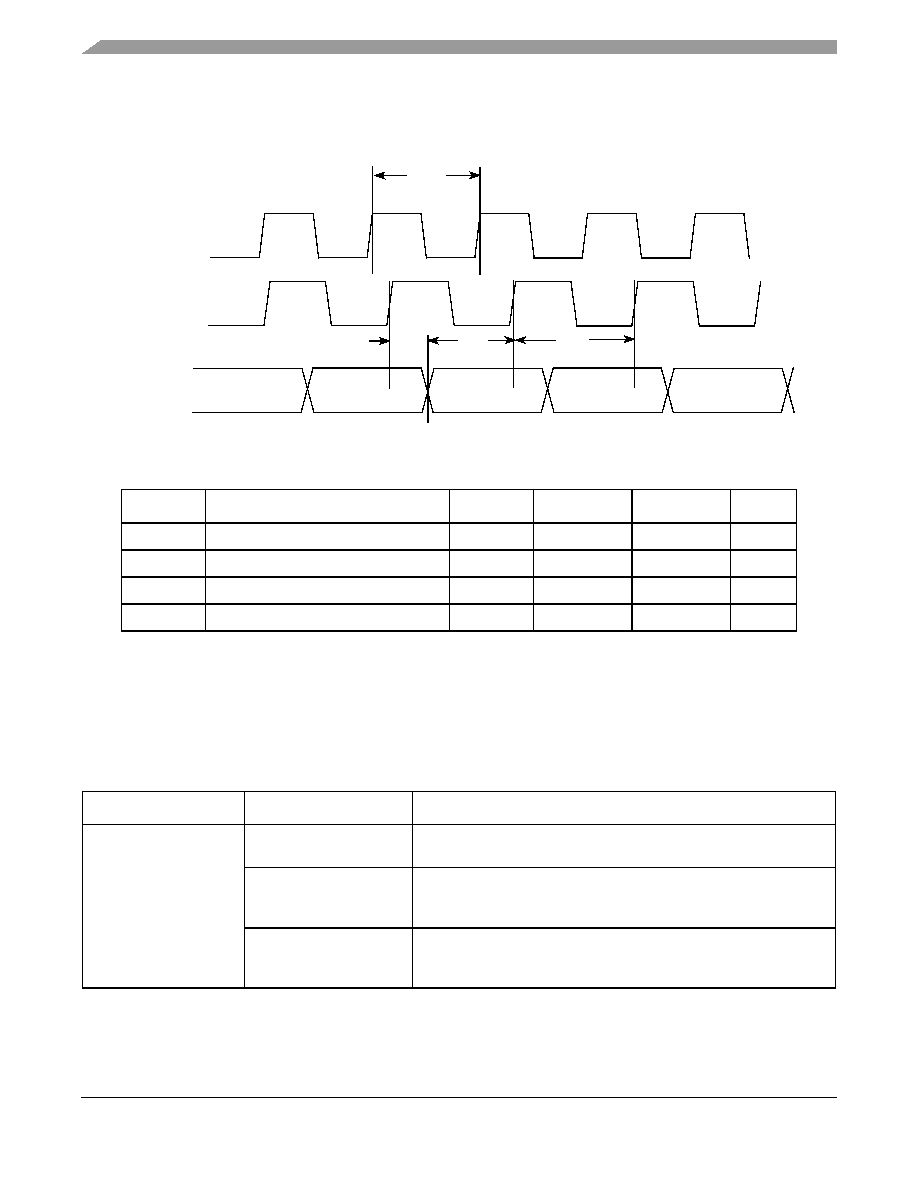
i.MX31/i.MX31L Advance Information, Rev. 1.4
106
Freescale Semiconductor
Preliminary
Electrical Characteristics
4.3.14.3
Electrical Characteristics
Figure 47
depicts the sensor interface timing, and
Table 46
lists the timing parameters.
Figure 47. Sensor Interface Timing Diagram
4.3.15
IPU
--
Display Interfaces
4.3.15.1
Supported Displays
Table 47
lists the supported displays by type, vendor, and model.
Table 46. Sensor Interface Timing Parameters
ID
Parameter
Symbol
Min.
Max.
Units
IP1
Sensor input clock frequency
Fmck
0.01
133
MHz
IP2
Data and control setup time
Tsu
5
≠
ns
IP3
Data and control holdup time
Thd
3
≠
ns
IP4
Sensor output (pixel) clock frequency
Fpck
0.01
133
MHz
Table 47. Supported Displays
Type
Vendor
Model
TFT displays
(memory-less)
Sharp (HR-TFT Super
Mobile LCD family)
LQ035Q7 DB02, LM019LC1Sxx
Samsung (QSIF and
QVGA TFT modules for
mobile phones)
LTS180S1-HF1, LTS180S3-HF1, LTS350Q1-PE1,
LTS350Q1-PD1, LTS220Q1-HE1
Toshiba (LTM series)
LTM022P806, LTM04C380K,
LTM018A02A, LTM020P332, LTM021P337, LTM019P334,
LTM022A783, LTM022A05ZZ
SENSB_MCLK
IP3
SENSB_DATA,
SENSB_VSYNC,
IP2
1/IP1
1/IP4
SENSB_PIX_CLK
(Sensor Input)
(Sensor Output)
SENSB_HSYNC
Electrical Characteristics
i.MX31/i.MX31L Advance Information, Rev. 1.4
Freescale Semiconductor
107
Preliminary
4.3.15.2
Synchronous Interfaces
4.3.15.2.1
Interface to Active Matrix TFT LCD Panels, Functional Description
Figure 48
depicts the LCD interface timing for a generic active matrix color TFT panel. In this figure
signals are shown with negative polarity. The sequence of events for active matrix interface timing is:
∑
DISPB_D3_CLK latches data into the panel on its negative edge (when positive polarity is
selected). In active mode, DISPB_D3_CLK runs continuously. This signal frequency could be
from 5 to 10 MHz depending on the panel type.
∑
DISPB_D3_HSYNC causes the panel to start a new line.
∑
DISPB_D3_VSYNC causes the panel to start a new frame. It always encompasses at least one
HSYNC pulse.
∑
DISPB_D3_DRDY acts like an output enable signal to the CRT display. This output enables the
data to be shifted onto the display. When disabled, the data is invalid and the trace is off.
Display controllers
Epson
S1D15xxx series, S1D19xxx series, S1D13713, S1D13715
Solomon Systech
SSD1301 (OLED), SSD1828 (LDCD)
Hitachi
HD66766, HD66772
ATI
W2300
Smart display modules
Epson
L1F10043 T, L1F10044 T, L1F10045 T, L2D22002, L2D20014,
L2F50032, L2D25001 T
Hitachi
120 160 65K/4096 C-STN (#3284 LTD-1398-2) based on HD 66766
controller
Densitron Europe LTD
All displays with MPU 80/68K series interface and serial peripheral
interface
Sharp
LM019LC1Sxx
Sony
ACX506AKM
Digital video encoders
(for TV)
Analog Devices
ADV7174/7179
Crystal (Cirrus Logic)
CS49xx series
Focus
FS453/4
Table 47. Supported Displays (continued)
Type
Vendor
Model
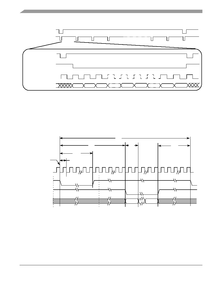
i.MX31/i.MX31L Advance Information, Rev. 1.4
108
Freescale Semiconductor
Preliminary
Electrical Characteristics
Figure 48. Interface Timing Diagram for TFT (Active Matrix) Panels
4.3.15.2.2
Interface to Active Matrix TFT LCD Panels, Electrical Characteristics
Figure 49
depicts the horizontal timing (timing of one line), including both the horizontal sync pulse and
the data. All figure parameters shown are programmable. The timing images correspond to inverse polarity
of the DISPB_D3_CLK signal and active-low polarity of the DISPB_D3_HSYNC, DISPB_D3_VSYNC
and DISPB_D3_DRDY signals.
Figure 49. TFT Panels Timing Diagram--Horizontal Sync Pulse
Figure 50
depicts the vertical timing (timing of one frame). All figure parameters shown are
programmable.
DISPB_D3_CLK
1
2
3
m
m-1
DISPB_D3_HSYNC
DISPB_D3_VSYNC
DISPB_D3_HSYNC
LINE 1
LINE 2
LINE 3
LINE 4
LINE n-1
LINE n
DISPB_D3_DRDY
DISPB_D3_DATA
DISPB_D3_HSYNC
DISPB_D3_DRDY
DISPB_D3_DATA
DISPB_D3_CLK
IP7
IP9
IP10
IP8
Start of line
IP5
IP6
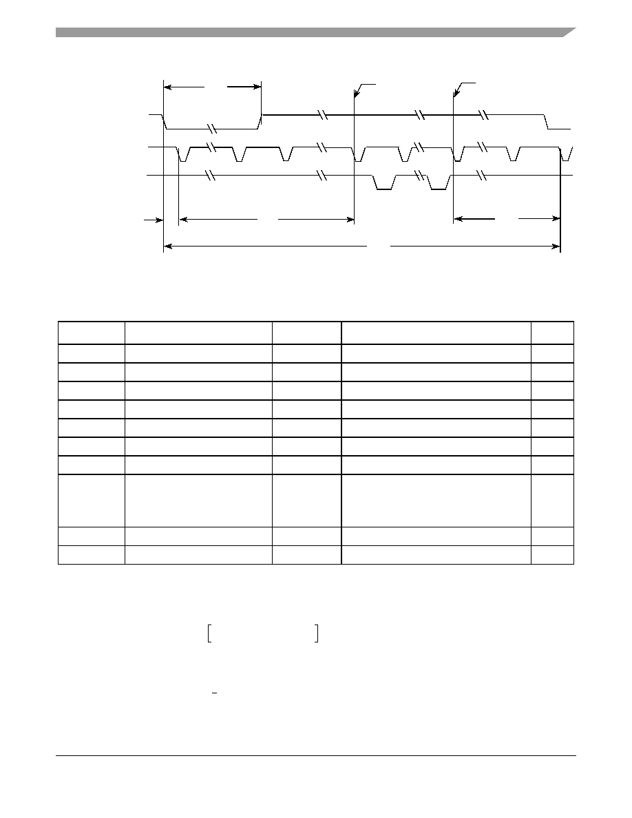
Electrical Characteristics
i.MX31/i.MX31L Advance Information, Rev. 1.4
Freescale Semiconductor
109
Preliminary
Figure 50. TFT Panels Timing Diagram--Vertical Sync Pulse
Table 48
shows timing parameters of signals presented in
Figure 49
and
Figure 50
.
Table 48. Synchronous Display Interface Timing Parameters--Pixel Level
ID
Parameter
Symbol
Value
Units
IP5
Display interface clock period
Tdicp
(
1
)
1
Display interface clock period immediate value.
Display interface clock period average value.
ns
IP6
Display pixel clock period
Tdpcp
(DISP3_IF_CLK_CNT_D+1) * Tdicp
ns
IP7
Screen width
Tsw
(SCREEN_WIDTH+1) * Tdpcp
ns
IP8
HSYNC width
Thsw
(H_SYNC_WIDTH+1) * Tdpcp
ns
IP9
Horizontal blank interval 1
Thbi1
BGXP * Tdpcp
ns
IP10
Horizontal blank interval 2
Thbi2
(SCREEN_WIDTH - BGXP - FW) * Tdpcp
ns
IP12
Screen height
Tsh
(SCREEN_HEIGHT+1) * Tsw
ns
IP13
VSYNC width
Tvsw
if V_SYNC_WIDTH_L = 0 than
(V_SYNC_WIDTH+1) * Tdpcp
else
(V_SYNC_WIDTH+1) * Tsw
ns
IP14
Vertical blank interval 1
Tvbi1
BGYP * Tsw
ns
IP15
Vertical blank interval 2
Tvbi2
(SCREEN_HEIGHT - BGYP - FH) * Tsw
ns
IP14
DISPB_D3_VSYNC
DISPB_D3_HSYNC
DISPB_D3_DRDY
Start of frame
End of frame
IP12
IP15
IP13
IP11
Tdicp
THSP_CLK
DISP3_IF_CLK_PER_WR
HSP_CLK_PERIOD
------------------------------------------------------------------
for integer
DISP3_IF_CLK_PER_WR
HSP_CLK_PERIOD
------------------------------------------------------------------
,
THSP_CLK floor
DISP3_IF_CLK_PER_WR
HSP_CLK_PERIOD
------------------------------------------------------------------
0.5 0.5
±
+
for fractional
DISP3_IF_CLK_PER_WR
HSP_CLK_PERIOD
------------------------------------------------------------------
,
=
Tdicp
THSP_CLK
DISP3_IF_CLK_PER_WR
HSP_CLK_PERIOD
------------------------------------------------------------------
=
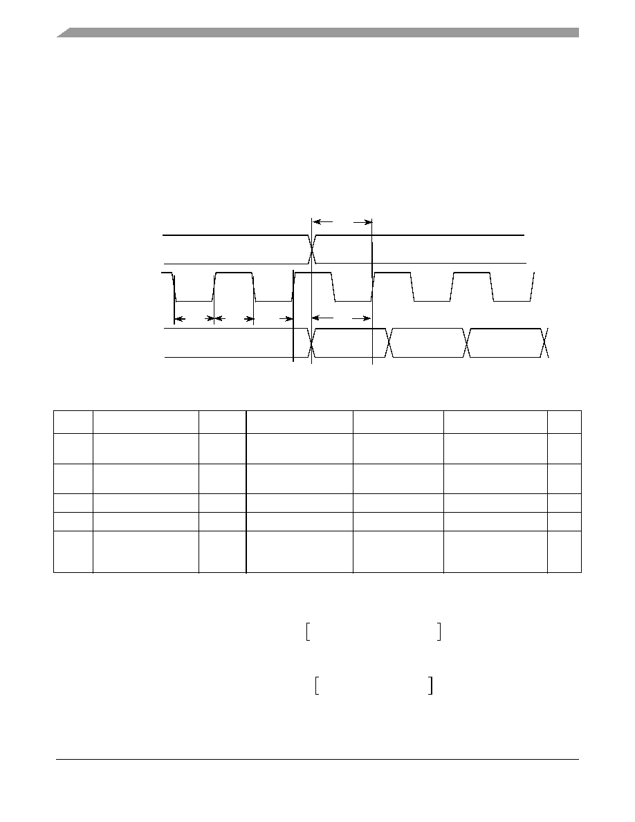
i.MX31/i.MX31L Advance Information, Rev. 1.4
110
Freescale Semiconductor
Preliminary
Electrical Characteristics
The SCREEN_WIDTH, SCREEN_HEIGHT, H_SYNC_WIDTH, V_SYNC_WIDTH, BGXP, BGYP and
V_SYNC_WIDTH_L parameters are programmed via the SDC_HOR_CONF, SDC_VER_CONF,
SDC_BG_POS Registers. The FW and FH parameters are programmed for the corresponding DMA
channel. The DISP3_IF_CLK_PER_WR, HSP_CLK_PERIOD and DISP3_IF_CLK_CNT_D parameters
are programmed via the DI_DISP3_TIME_CONF, DI_HSP_CLK_PER and DI_DISP_ACC_CC
Registers.
Figure 51
depicts the synchronous display interface timing for access level, and
Table 49
lists the timing
parameters. The DISP3_IF_CLK_DOWN_WR and DISP3_IF_CLK_UP_WR parameters are set via the
DI_DISP3_TIME_CONF Register.
Figure 51. Synchronous Display Interface Timing Diagram--Access Level
Table 49. Synchronous Display Interface Timing Parameters--Access Level
ID
Parameter
Symbol
Min
Typ
1
1
The exact conditions have not been finalized, but will likely match the current customer requirement for their specific display.
These conditions may be chip specific.
Max
Units
IP16
Display interface clock
low time
Tckl
Tdicd-Tdicu-1.5
Tdicd
2
-Tdicu
3
2
Display interface clock down time
3
Display interface clock up time
where CEIL(X) rounds the elements of X to the nearest integers towards infinity.
Tdicd-Tdicu+1.5
ns
IP17
Display interface clock
high time
Tckh
Tdicp-Tdicd+Tdicu-1.5
Tdicp-Tdicd+Tdicu
Tdicp-Tdicd+Tdicu+1.5
ns
IP18
Data setup time
Tdsu
Tdicd-3.5
Tdicu
≠
ns
IP19
Data holdup time
Tdhd
Tdicp-Tdicd-3.5
Tdicp-Tdicu
ns
IP20
Control signals setup
time to display interface
clock
Tcsu
Tdicd-3.5
Tdicu
ns
IP19
DISPB_D3_CLK
DISPB_DATA
IP18
IP20
DISPB_D3_VSYNC
IP17
IP16
DISPB_D3_DRDY
DISPB_D3_HSYNC
other controls
Tdicd
1
2
---
THSP_CLK ceil
2 DISP3_IF_CLK_DOWN_WR
HSP_CLK_PERIOD
---------------------------------------------------------------------------------
=
Tdicu
1
2
---
THSP_CLK ceil
2 DISP3_IF_CLK_UP_WR
HSP_CLK_PERIOD
----------------------------------------------------------------------
=
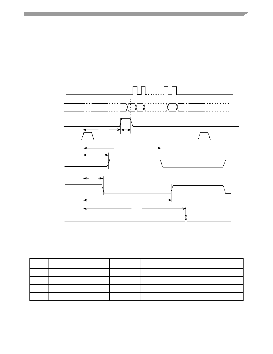
Electrical Characteristics
i.MX31/i.MX31L Advance Information, Rev. 1.4
Freescale Semiconductor
111
Preliminary
4.3.15.3
Interface to Sharp HR-TFT Panels
Figure 52
depicts the Sharp HR-TFT panel interface timing, and
Table 50
lists the timing parameters. The
CLS_RISE_DELAY, CLS_FALL_DELAY, PS_FALL_DELAY, PS_RISE_DELAY,
REV_TOGGLE_DELAY parameters are defined in the SDC_SHARP_CONF_1 and
SDC_SHARP_CONF_2 registers. For other Sharp interface timing characteristics, refer to
Section 4.3.15.2.2, "Interface to Active Matrix TFT LCD Panels, Electrical Characteristics" on page 108.
The timing images correspond to straight polarity of the Sharp signals.
Figure 52. Sharp HR-TFT Panel Interface Timing Diagram--Pixel Level
Table 50. Sharp Synchronous Display Interface Timing Parameters--Pixel Level
ID
Parameter
Symbol
Value
Units
IP21
SPL rise time
Tsplr
(BGXP - 1) * Tdpcp
ns
IP22
CLS rise time
Tclsr
CLS_RISE_DELAY * Tdpcp
ns
IP23
CLS fall time
Tclsf
CLS_FALL_DELAY * Tdpcp
ns
IP24
CLS rise and PS fall time
Tpsf
PS_FALL_DELAY * Tdpcp
ns
D1
D2
DISPB_D3_CLK
DISPB_D3_DATA
DISPB_D3_SPL
DISPB_D3_HSYNC
DISPB_D3_CLS
DISPB_D3_PS
DISPB_D3_REV
1 DISPB_D3_CLK period
IP26
D320
Horizontal timing
IP22
IP23
IP25
IP21
IP24
Example is drawn with FW+1=320 pixel/line, FH+1=240 lines.
SPL pulse width is fixed and aligned to the first data of the line.
REV toggles every HSYNC period.

i.MX31/i.MX31L Advance Information, Rev. 1.4
112
Freescale Semiconductor
Preliminary
Electrical Characteristics
4.3.15.4
Synchronous Interface to Dual-Port Smart Displays
Functionality and electrical characteristics of the synchronous interface to dual-port smart displays are
identical to parameters of the synchronous interface. See
Section 4.3.15.2.2, "Interface to Active Matrix
TFT LCD Panels, Electrical Characteristics
"
on page 108
.
4.3.15.4.1
Interface to a TV Encoder,
Functional Description
The interface has an 8-bit data bus, transferring a single 8-bit value (Y/U/V) in each cycle. The bits
D7≠D0 of the value are mapped to bits LD17≠LD10 of the data bus, respectively.
Figure 53
depicts the
interface timing,
∑
The frequency of the clock DISPB_D3_CLK is 27 MHz (within 10%).
∑
The DISPB_D3_HSYNC, DISPB_D3_VSYNC and DISPB_D3_DRDY signals are active low.
∑
The transition to the next row is marked by the negative edge of the DISPB_D3_HSYNC signal. It
remains low for a single clock cycle.
∑
The transition to the next field/frame is marked by the negative edge of the DISPB_D3_VSYNC
signal. It remains low for at least one clock cycle.
-- At a transition to an odd field (of the next frame), the negative edges of DISPB_D3_VSYNC
and DISPB_D3_HSYNC coincide.
-- At a transition to an even field (of the same frame), they do not coincide.
∑
The active intervals--during which data is transferred--are marked by the DISPB_D3_HSYNC
signal being high.
IP25
PS rise time
Tpsr
PS_RISE_DELAY * Tdpcp
ns
IP26
REV toggle time
Trev
REV_TOGGLE_DELAY * Tdpcp
ns
Table 50. Sharp Synchronous Display Interface Timing Parameters--Pixel Level (continued)
ID
Parameter
Symbol
Value
Units
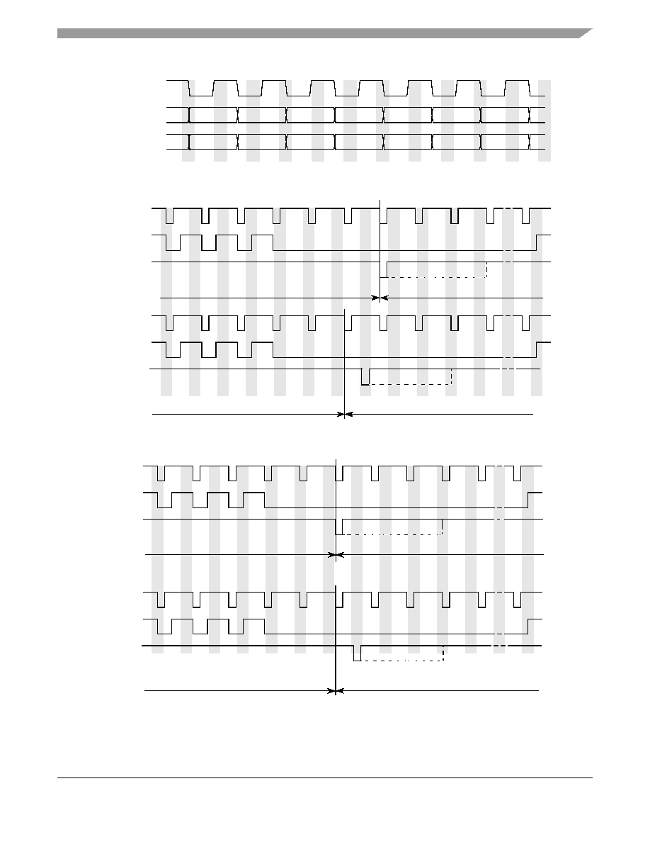
Electrical Characteristics
i.MX31/i.MX31L Advance Information, Rev. 1.4
Freescale Semiconductor
113
Preliminary
Figure 53. TV Encoder Interface Timing Diagram
DISPB_D3_CLK
DISPB_D3_HSYNC
DISPB_DATA
DISPB_D3_VSYNC
Cb
Y
Cr
Cb
Y
Cr
Y
Pixel Data Timing
Line and Field Timing - NTSC
Even Field
Odd Field
Odd Field
Even Field
624
621
311
308
Line and Field Timing - PAL
DISPB_D3_HSYNC
DISPB_D3_DRDY
DISPB_D3_VSYNC
DISPB_D3_HSYNC
DISPB_D3_DRDY
DISPB_D3_VSYNC
Even Field
Odd Field
Odd Field
Even Field
1
523
262
261
DISPB_D3_DRDY
DISPB_D3_HSYNC
DISPB_D3_DRDY
DISPB_D3_VSYNC
DISPB_D3_HSYNC
DISPB_D3_VSYNC
524
525
2
3
4
10
263
264
265
266
267
268
269
273
622
623
625
1
2
23
309
310
312
313
314
336
5
6
3
4
316
315
DISPB_D3_DRDY

i.MX31/i.MX31L Advance Information, Rev. 1.4
114
Freescale Semiconductor
Preliminary
Electrical Characteristics
4.3.15.4.2
Interface to a TV Encoder,
Electrical Characteristics
The timing characteristics of the TV encoder interface are identical to the synchronous display
characteristics. See
Section 4.3.15.2.2, "Interface to Active Matrix TFT LCD Panels, Electrical
Characteristics
"
on page 108
.
4.3.15.5
Asynchronous Interfaces
4.3.15.5.1
Parallel Interfaces,
Functional Description
The IPU supports the following asynchronous parallel interfaces:
∑
System 80 interface
-- Type 1 (sampling with the chip select signal) with and without byte enable signals.
-- Type 2 (sampling with the read and write signals) with and without byte enable signals.
∑
System 68k interface
-- Type 1 (sampling with the chip select signal) with or without byte enable signals.
-- Type 2 (sampling with the read and write signals) with or without byte enable signals.
For each of four system interfaces, there are three burst modes:
1. Burst mode without a separate clock. The burst length is defined by the corresponding parameters
of the IDMAC (when data is transferred from the system memory) of by the HBURST signal (when
the MCU directly accesses the display via the slave AHB bus). For system 80 and system 68k type
1 interfaces, data is sampled by the CS signal and other control signals changes only when transfer
direction is changed during the burst. For type 2 interfaces, data is sampled by the WR/RD signals
(system 80) or by the ENABLE signal (system 68k) and the CS signal stays active during the whole
burst.
2. Burst mode with the separate clock DISPB_BCLK. In this mode, data is sampled with the
DISPB_BCLK clock. The CS signal stays active during whole burst transfer. Other controls are
changed simultaneously with data when the bus state (read, write or wait) is altered. The CS
signals and other controls move to non-active state after burst has been completed.
3. Single access mode. In this mode, slave AHB and DMA burst are broken to single accesses. The
data is sampled with CS or other controls according the interface type as described above. All
controls (including CS) become non-active for one display interface clock after each access. This
mode corresponds to the ATI single access mode.
Both system 80 and system 68k interfaces are supported for all described modes as depicted in
Figure 54
,
Figure 55
,
Figure 56
, and
Figure 57
. These timing images correspond to active-low DISPB_D#_CS,
DISPB_D#_WR and DISPB_D#_RD signals.
Additionally, the IPU allows a programmable pause between two burst. The pause is defined in the
HSP_CLK cycles. It allows to avoid timing violation between two sequential bursts or two accesses to
different displays. The range of this pause is from 4 to 19 HSP_CLK cycles.
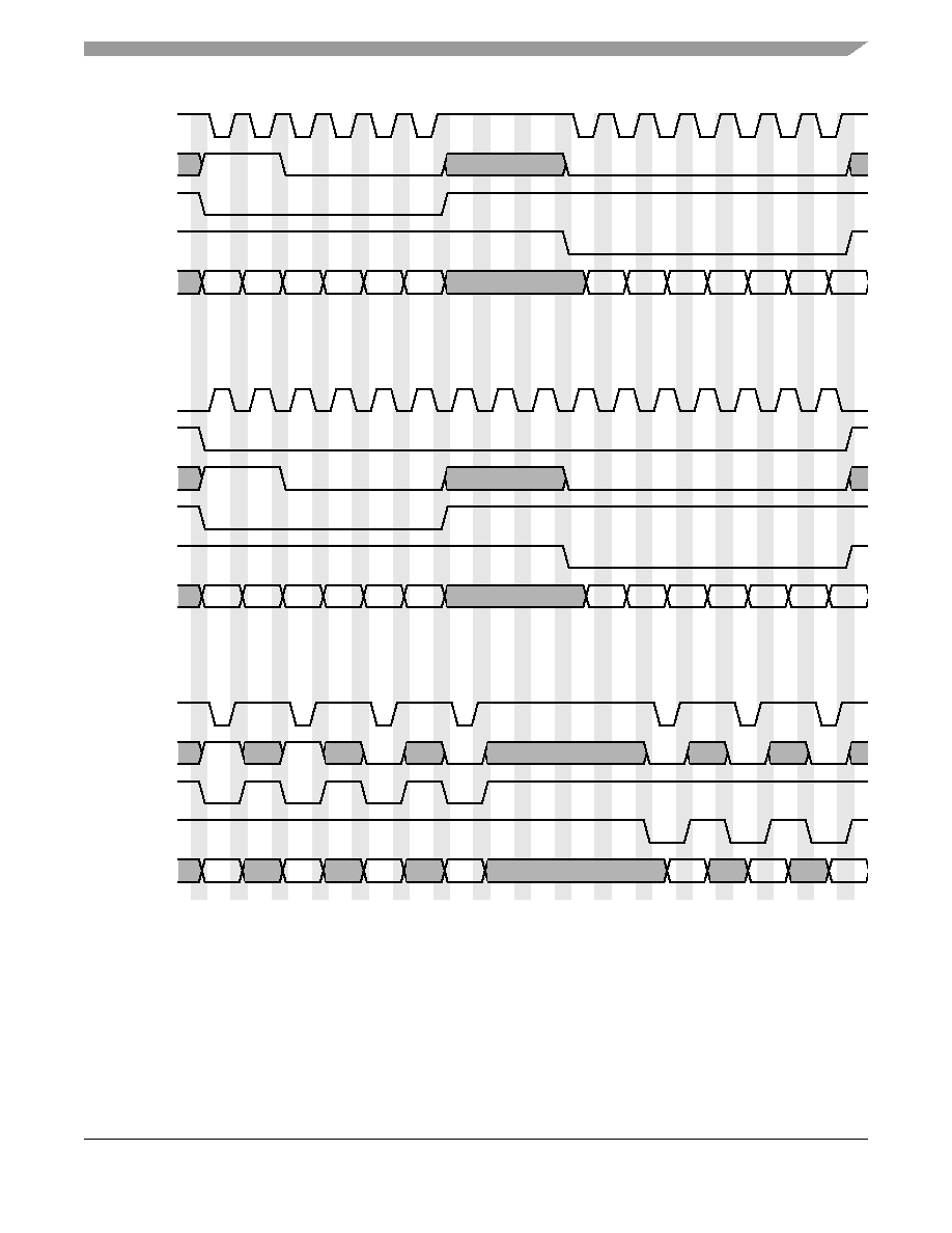
Electrical Characteristics
i.MX31/i.MX31L Advance Information, Rev. 1.4
Freescale Semiconductor
115
Preliminary
Figure 54. Asynchronous Parallel System 80 Interface (Type 1) Burst Mode Timing Diagram
DISPB_D#_CS
DISPB_PAR_RS
DISPB_WR
DISPB_RD
DISPB_DATA
DISPB_BCLK
DISPB_D#_CS
DISPB_PAR_RS
DISPB_WR
DISPB_RD
DISPB_DATA
DISPB_D#_CS
DISPB_PAR_RS
DISPB_WR
DISPB_RD
DISPB_DATA
Burst access mode with sampling by CS signal
Burst access mode with sampling by separate burst clock (BCLK)
Single access mode (all control signals are not active for one display interface clock after each display access)
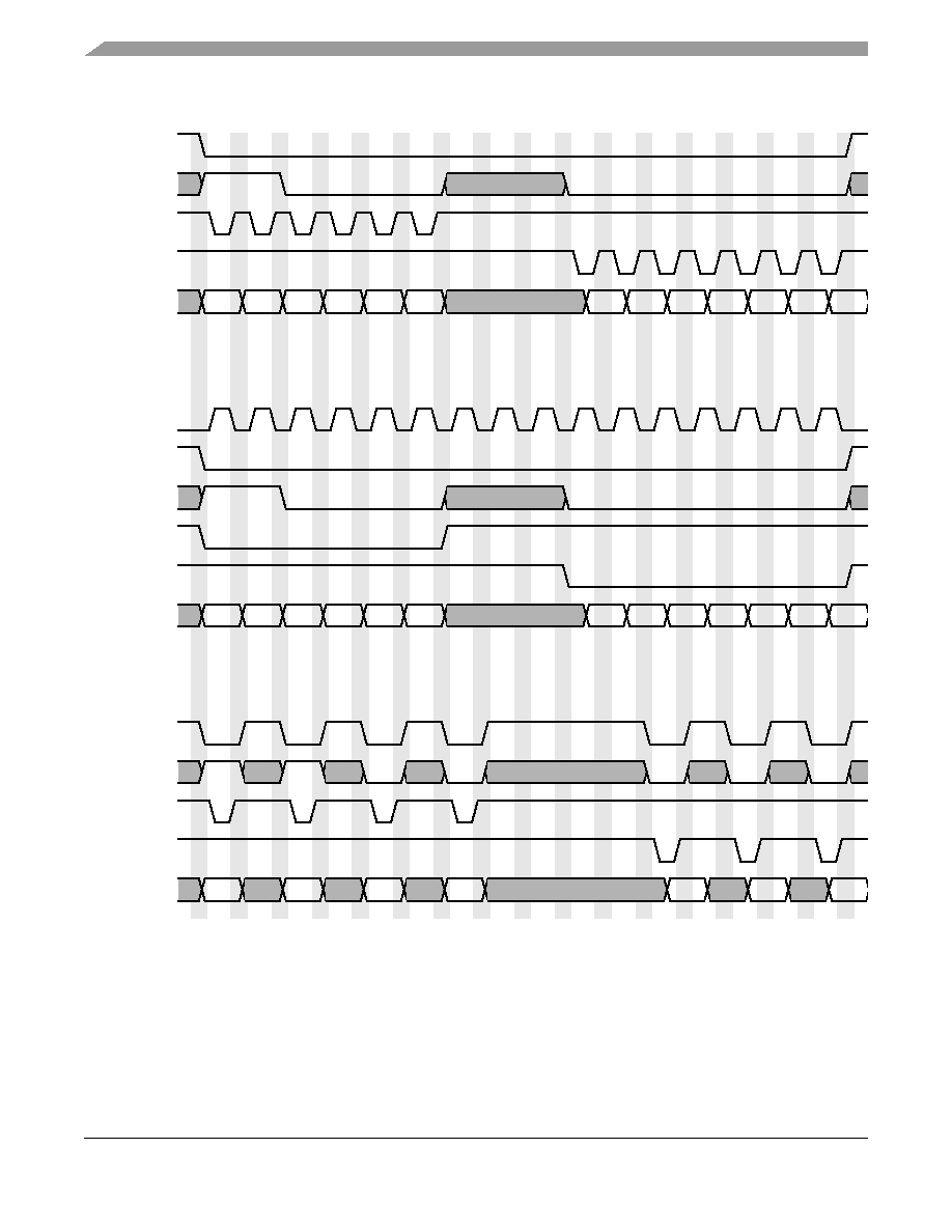
i.MX31/i.MX31L Advance Information, Rev. 1.4
116
Freescale Semiconductor
Preliminary
Electrical Characteristics
Figure 55. Asynchronous Parallel System 80 Interface (Type 2) Burst Mode Timing Diagram
DISPB_D#_CS
DISPB_PAR_RS
DISPB_WR
DISPB_RD
DISPB_DATA
DISPB_BCLK
DISPB_D#_CS
DISPB_PAR_RS
DISPB_WR
DISPB_RD
DISPB_DATA
DISPB_D#_CS
DISPB_PAR_RS
DISPB_WR
DISPB_RD
DISPB_DATA
Burst access mode with sampling by WR/RD signals
Burst access mode with sampling by separate burst clock (BCLK)
Single access mode (all control signals are not active for one display interface clock after each display access)
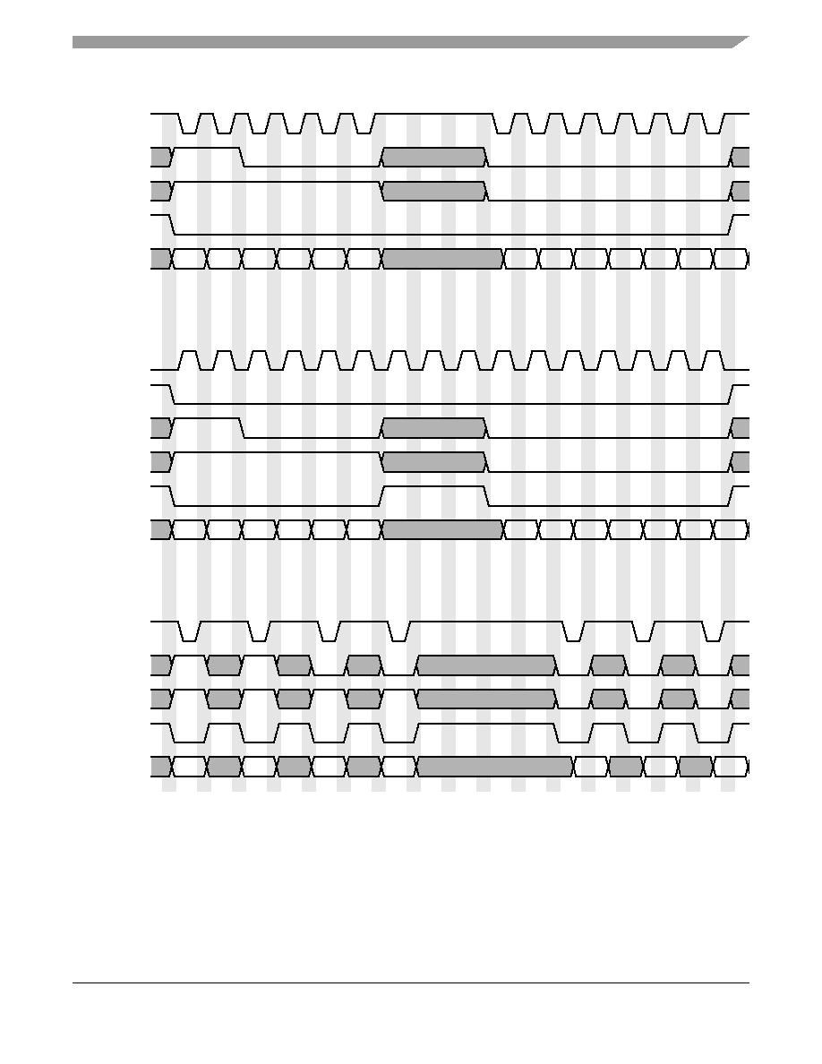
Electrical Characteristics
i.MX31/i.MX31L Advance Information, Rev. 1.4
Freescale Semiconductor
117
Preliminary
Figure 56. Asynchronous Parallel System 68k Interface (Type 1) Burst Mode Timing Diagram
DISPB_D#_CS
DISPB_WR
DISPB_RD
DISPB_DATA
DISPB_BCLK
DISPB_D#_CS
DISPB_PAR_RS
DISPB_WR
DISPB_RD
DISPB_DATA
DISPB_D#_CS
DISPB_WR
DISPB_RD
DISPB_DATA
(READ/WRITE)
(ENABLE)
DISPB_PAR_RS
DISPB_PAR_RS
(READ/WRITE)
(ENABLE)
(READ/WRITE)
(ENABLE)
Burst access mode with sampling by CS signal
Burst access mode with sampling by separate burst clock (BCLK)
Single access mode (all control signals are not active for one display interface clock after each display access)
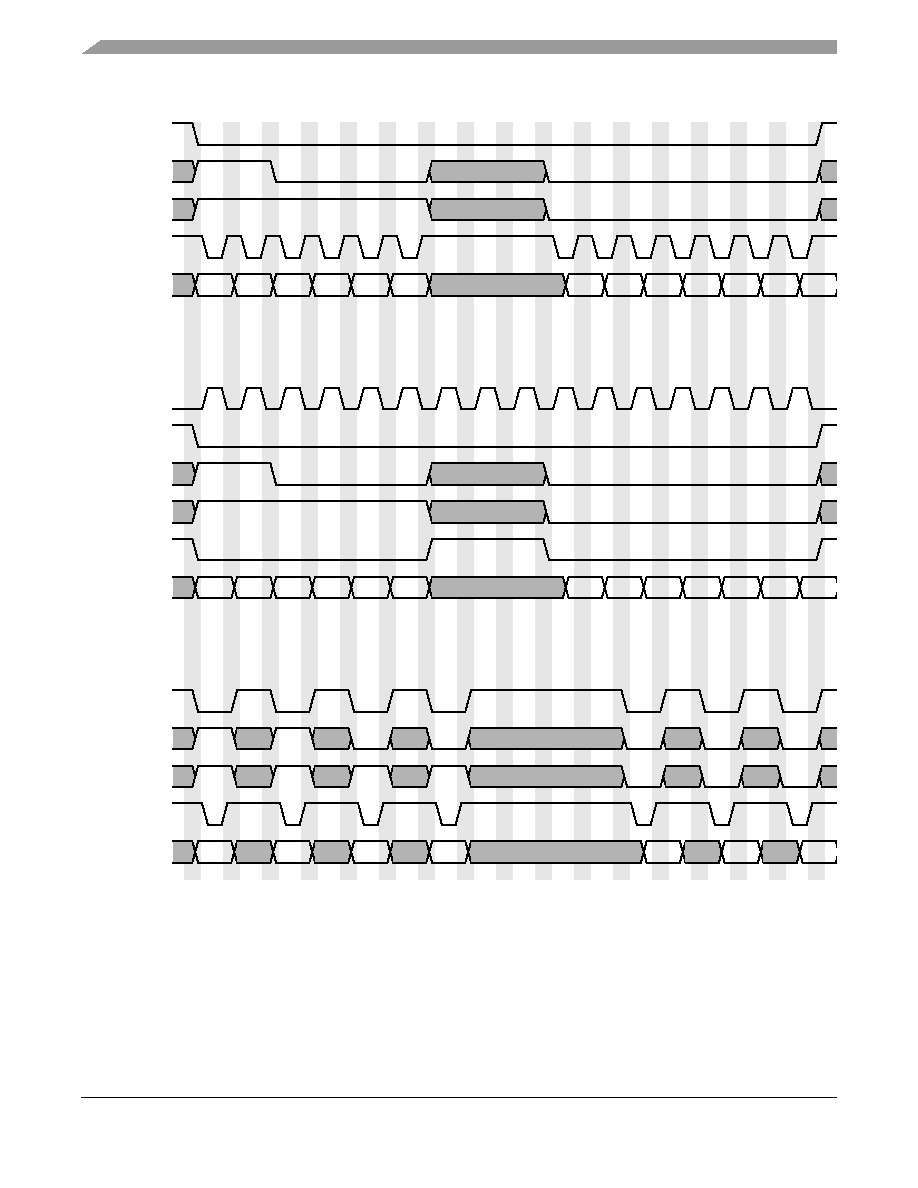
i.MX31/i.MX31L Advance Information, Rev. 1.4
118
Freescale Semiconductor
Preliminary
Electrical Characteristics
Figure 57. Asynchronous Parallel System 68k Interface (Type 2) Burst Mode TIming Diagram
Display read operation can be performed with wait states when each read access takes up to 4 display
interface clock cycles according to the DISP0_RD_WAIT_ST parameter in the
DI_DISP0_TIME_CONF_3, DI_DISP1_TIME_CONF_3, DI_DISP2_TIME_CONF_3 Registers.
Figure 58
shows timing of the parallel interface with read wait states.
DISPB_D#_CS
DISPB_PAR_RS
DISPB_WR
DISPB_RD
DISPB_DATA
DISPB_BCLK
DISPB_D#_CS
DISPB_PAR_RS
DISPB_WR
DISPB_RD
DISPB_DATA
DISPB_D#_CS
DISPB_PAR_RS
DISPB_WR
DISPB_RD
DISPB_DATA
(READ/WRITE)
(ENABLE)
(READ/WRITE)
(ENABLE)
(READ/WRITE)
(ENABLE)
Burst access mode with sampling by ENABLE signal
Burst access mode with sampling by separate burst clock (BCLK)
Single access mode (all control signals are not active for one display interface clock after each display access)
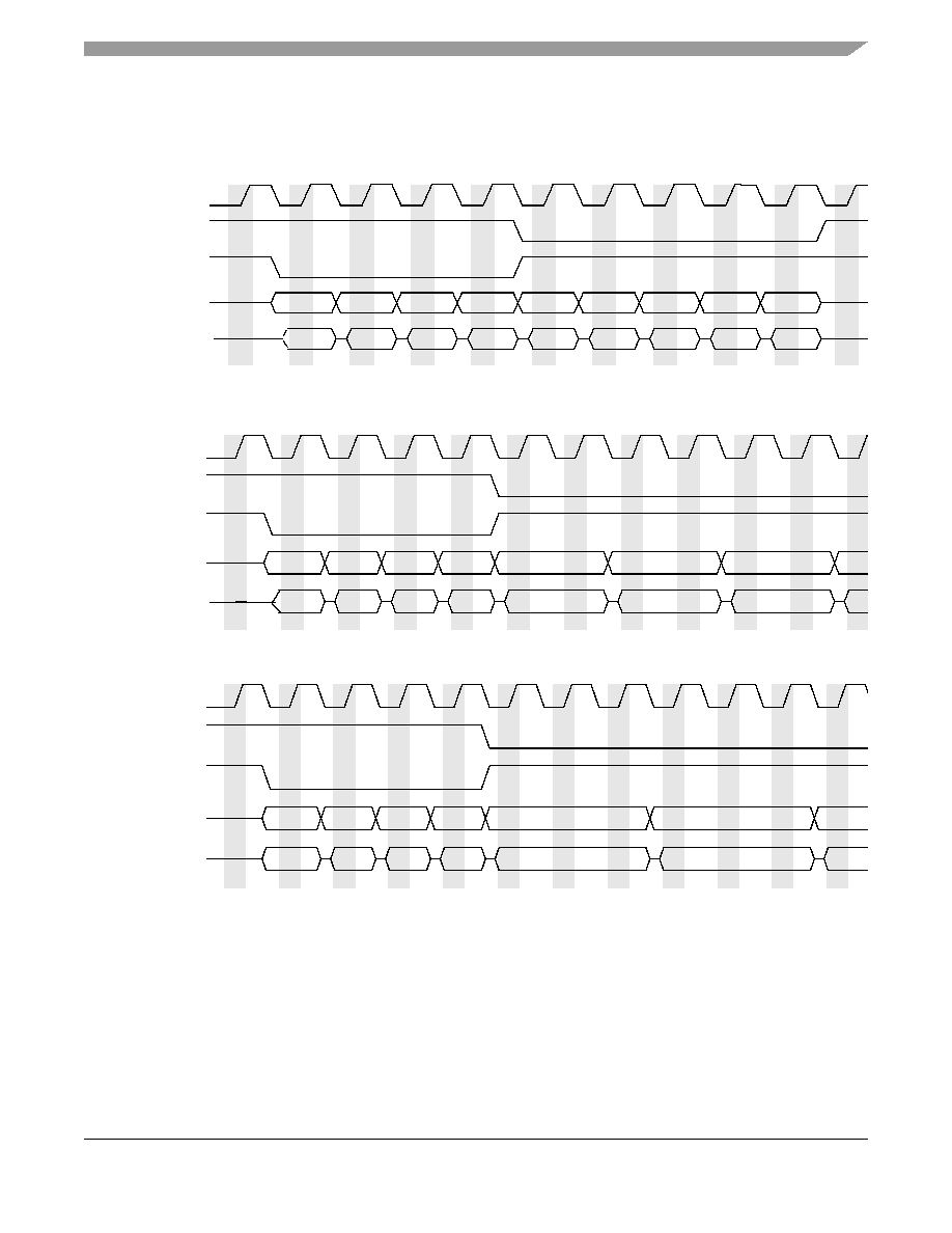
Electrical Characteristics
i.MX31/i.MX31L Advance Information, Rev. 1.4
Freescale Semiconductor
119
Preliminary
Figure 58. Parallel Interface Timing Diagram--Read Wait States
4.3.15.5.2
Parallel Interfaces
, Electrical Characteristics
Figure 59
,
Figure 61
,
Figure 60
, and
Figure 62
depict timing of asynchronous parallel interfaces based on
the system 80 and system 68k interfaces.
Table 51
lists the timing parameters at display access level. All
timing images are based on active low control signals (signals polarity is controlled via the
DI_DISP_SIG_POL Register).
WRITE OPERATION
READ OPERATION
DISPB_D#_CS
DISPB_RD
DISPB_WR
DISPB_PAR_RS
DISPB_D#_CS
DISPB_RD
DISPB_WR
DISPB_PAR_RS
DISPB_DATA
DISPB_D#_CS
DISPB_RD
DISPB_WR
DISPB_PAR_RS
DISPB_DATA
DISPB_DATA
DISP0_RD_WAIT_ST=00
DISP0_RD_WAIT_ST=01
DISP0_RD_WAIT_ST=10
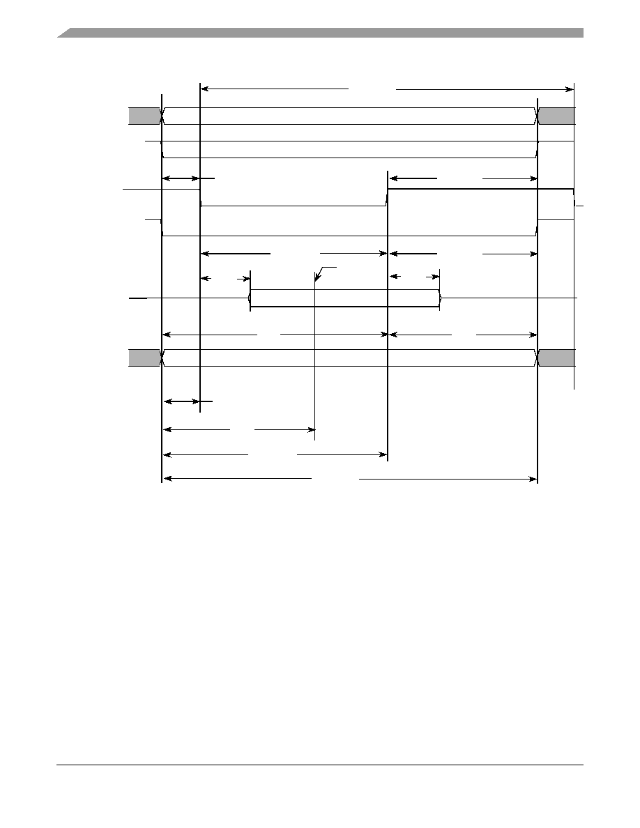
i.MX31/i.MX31L Advance Information, Rev. 1.4
120
Freescale Semiconductor
Preliminary
Electrical Characteristics
Figure 59. Asynchronous Parallel System 80 Interface (Type 1) Timing Diagram
IP28, IP27
Read Data
IP32, IP30
IP37
IP38
DISPB_PAR_RS
DISPB_DATA
DISPB_DATA
DISPB_WR (WRITE_L)
(Input)
(Output)
IP35, IP33
IP36, IP34
IP31, IP29
IP40
IP39
IP46,IP44
IP47
IP45, IP43
IP42, IP41
DISPB_RD (READ_L)
DISPB_D#_CS
DISPB_DATA[16]
DISPB_DATA[17]
read point
(WRITE_H)
(READ_H)
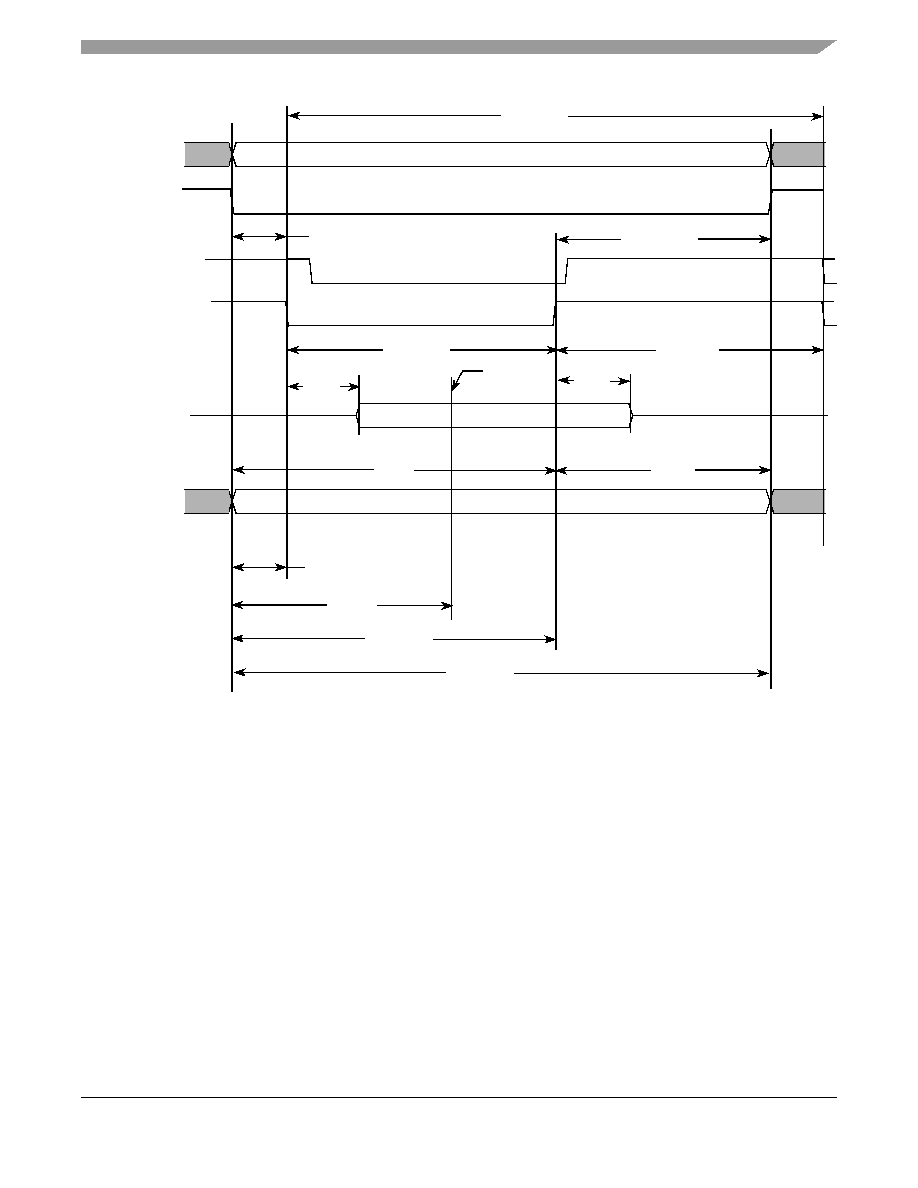
Electrical Characteristics
i.MX31/i.MX31L Advance Information, Rev. 1.4
Freescale Semiconductor
121
Preliminary
Figure 60. Asynchronous Parallel System 80 Interface (Type 2) Timing Diagram
IP28, IP27
Read Data
IP32, IP30
DISPB_PAR_RS
DISPB_DATA
DISPB_DATA
DISPB_WR (WRITE_L)
(Input)
(Output)
IP36, IP34
IP31, IP29
IP40
IP39
IP47
IP45, IP43
IP42, IP41
DISPB_RD (READ_L)
DISPB_D#_CS
DISPB_DATA[16]
DISPB_DATA[17]
(WRITE_H)
(READ_H)
IP38
IP35, IP33
IP37
read point
IP46,IP44
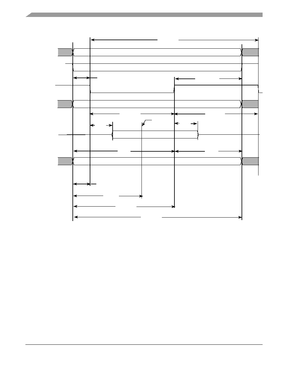
i.MX31/i.MX31L Advance Information, Rev. 1.4
122
Freescale Semiconductor
Preliminary
Electrical Characteristics
Figure 61. Asynchronous Parallel System 68k Interface (Type 1) Timing Diagram
IP28, IP27
Read Data
IP32, IP30
IP37
IP38
DISPB_PAR_RS
DISPB_DATA
DISPB_DATA
DISPB_WR
(Input)
(Output)
IP35,IP33
IP36, IP34
IP31, IP29
IP40
IP39
IP47
IP45, IP43
IP42, IP41
DISPB_RD (ENABLE_L)
DISPB_D#_CS
(READ/WRITE)
DISPB_DATA[17]
(ENABLE_H)
read point
IP46,IP44
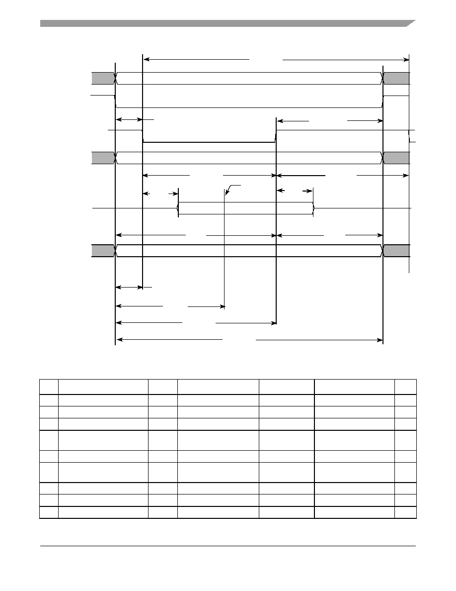
Electrical Characteristics
i.MX31/i.MX31L Advance Information, Rev. 1.4
Freescale Semiconductor
123
Preliminary
Figure 62. Asynchronous Parallel System 68k Interface (Type 2) Timing Diagram
Table 51. Asynchronous Parallel Interface Timing Parameters--Access Level
ID
Parameter
Symbol
Min.
Typ.
1
Max.
Units
IP27 Read system cycle time
Tcycr
Tdicpr-1.5
Tdicpr
2
Tdicpr+1.5
ns
IP28 Write system cycle time
Tcycw
Tdicpw-1.5
Tdicpw
3
Tdicpw+1.5
ns
IP29 Read low pulse width
Trl
Tdicdr-Tdicur-1.5
Tdicdr
4
-Tdicur
5
Tdicdr-Tdicur+1.5
ns
IP30 Read high pulse width
Trh
Tdicpr-Tdicdr+Tdicur-1.5
Tdicpr-Tdicdr+
Tdicur
Tdicpr-Tdicdr+Tdicur+1.5
ns
IP31 Write low pulse width
Twl
Tdicdw-Tdicuw-1.5
Tdicdw
6
-Tdicuw
7
Tdicdw-Tdicuw+1.5
ns
IP32 Write high pulse width
Twh
Tdicpw-Tdicdw+
Tdicuw-1.5
Tdicpw-Tdicdw+
Tdicuw
Tdicpw-Tdicdw+
Tdicuw+1.5
ns
IP33 Controls setup time for read
Tdcsr
Tdicur-1.5
Tdicur
≠
ns
IP34 Controls hold time for read
Tdchr
Tdicpr-Tdicdr-1.5
Tdicpr-Tdicdr
≠
ns
IP35 Controls setup time for write
Tdcsw
Tdicuw-1.5
Tdicuw
≠
ns
IP28, IP27
Read Data
IP32, IP30
IP37
IP38
DISPB_PAR_RS
DISPB_DATA
DISPB_DATA
DISPB_WR
(Input)
(Output)
IP35,IP33
IP36, IP34
IP31, IP29
IP40
IP39
IP45, IP43
IP42, IP41
DISPB_RD (ENABLE_L)
DISPB_D#_CS
(READ/WRITE)
DISPB_DATA[17]
(ENABLE_H)
read point
IP46,IP44
IP47
i.MX31/i.MX31L Advance Information, Rev. 1.4
124
Freescale Semiconductor
Preliminary
Electrical Characteristics
IP36 Controls hold time for write
Tdchw
Tdicpw-Tdicdw-1.5
Tdicpw-Tdicdw
≠
ns
IP37 Slave device data delay
8
Tracc
0
≠
Tdrp
9
-Tlbd
10
-Tdicur-1.5
ns
IP38 Slave device data hold time
8
Troh
Tdrp-Tlbd-Tdicdr+1.5
≠
Tdicpr-Tdicdr-1.5
ns
IP39 Write data setup time
Tds
Tdicdw-1.5
Tdicdw
≠
ns
IP40 Write data hold time
Tdh
Tdicpw-Tdicdw-1.5
Tdicpw-Tdicdw
≠
ns
IP41 Read period
2
Tdicpr
Tdicpr-1.5
Tdicpr
Tdicpr+1.5
ns
IP42 Write period
3
Tdicpw
Tdicpw-1.5
Tdicpw
Tdicpw+1.5
ns
IP43 Read down time
4
Tdicdr
Tdicdr-1.5
Tdicdr
Tdicdr+1.5
ns
IP44 Read up time
5
Tdicur
Tdicur-1.5
Tdicur
Tdicur+1.5
ns
IP45 Write down time
6
Tdicdw
Tdicdw-1.5
Tdicdw
Tdicdw+1.5
ns
IP46 Write up time
7
Tdicuw
Tdicuw-1.5
Tdicuw
Tdicuw+1.5
ns
IP47 Read time point
9
Tdrp
Tdrp-1.5
Tdrp
Tdrp+1.5
ns
1
The exact conditions have not been finalized, but will likely match the current customer requirement for their specific display.
These conditions may be chip specific.
2
Display interface clock period value for read:
3
Display interface clock period value for write:
4
Display interface clock down time for read:
5
Display interface clock up time for read:
6
Display interface clock down time for write:
7
Display interface clock up time for write:
8
This parameter is a requirement to the display connected to the IPU
9
Data read point
10
Loopback delay Tlbd is the cumulative propagation delay of read controls and read data. It includes an IPU output delay, a
chip-level output delay, board delays, a chip-level input delay, an IPU input delay. This value is chip specific.
Table 51. Asynchronous Parallel Interface Timing Parameters--Access Level (continued)
ID
Parameter
Symbol
Min.
Typ.
1
Max.
Units
Tdicpr
THSP_CLK ceil
DISP#_IF_CLK_PER_RD
HSP_CLK_PERIOD
----------------------------------------------------------------
=
Tdicpw
THSP_CLK ceil
DISP#_IF_CLK_PER_WR
HSP_CLK_PERIOD
------------------------------------------------------------------
=
Tdicdr
1
2
---
THSP_CLK ceil
2 DISP#_IF_CLK_DOWN_RD
HSP_CLK_PERIOD
-------------------------------------------------------------------------------
=
Tdicur
1
2
---
THSP_CLK ceil
2 DISP#_IF_CLK_UP_RD
HSP_CLK_PERIOD
--------------------------------------------------------------------
=
Tdicdw
1
2
---
THSP_CLK ceil
2 DISP#_IF_CLK_DOWN_WR
HSP_CLK_PERIOD
---------------------------------------------------------------------------------
=
Tdicuw
1
2
---
THSP_CLK ceil
2 DISP#_IF_CLK_UP_WR
HSP_CLK_PERIOD
----------------------------------------------------------------------
=
Tdrp
THSP_CLK ceil
DISP#_READ_EN
HSP_CLK_PERIOD
--------------------------------------------------
=
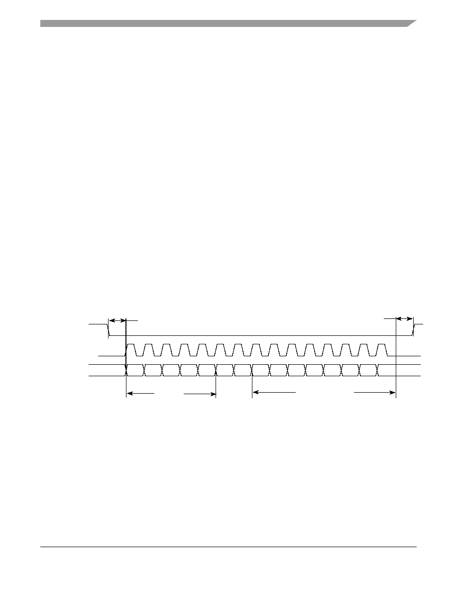
Electrical Characteristics
i.MX31/i.MX31L Advance Information, Rev. 1.4
Freescale Semiconductor
125
Preliminary
The DISP#_IF_CLK_PER_WR, DISP#_IF_CLK_PER_RD, HSP_CLK_PERIOD,
DISP#_IF_CLK_DOWN_WR, DISP#_IF_CLK_UP_WR, DISP#_IF_CLK_DOWN_RD,
DISP#_IF_CLK_UP_RD and DISP#_READ_EN parameters are programmed via the
DI_DISP#_TIME_CONF_1, DI_DISP#_TIME_CONF_2 and DI_HSP_CLK_PER Registers.
4.3.15.5.3
Serial Interfaces
, Functional Description
The IPU supports the following types of asynchronous serial interfaces:
∑
3-wire (with bidirectional data line)
∑
4-wire (with separate data input and output lines)
∑
5-wire type 1 (with sampling RS by the serial clock)
∑
5-wire type 2 (with sampling RS by the chip select signal)
Figure 63
depicts timing of the 3-wire serial interface. The timing images correspond to active-low
DISPB_D#_CS signal and the straight polarity of the DISPB_SD_D_CLK signal.
For this interface, a bidirectional data line is used outside the chip. The IPU still uses separate input and
output data lines (IPP_IND_DISPB_SD_D and IPP_DO_DISPB_SD_D). The I/O mux should provide
joining the internal data lines to the bidirectional external line according to the IPP_OBE_DISPB_SD_D
signal provided by the IPU.
Each data transfer can be preceded by an optional preamble with programmable length and contents. The
preamble is followed by read/write (RW) and address (RS) bits. The order of the these bits is
programmable. The RW bit can be disabled. The following data can consist of one word or of a whole
burst. The interface parameters are controlled by the DI_SER_DISP1_CONF and DI_SER_DISP2_CONF
Registers.
Figure 63. 3-wire Serial Interface Timing Diagram
Figure 64
depicts timing of the 4-wire serial interface. For this interface, there are separate input and output
data lines both inside and outside the chip.
Preamble
DISPB_D#_CS
DISPB_SD_D_CLK
DISPB_SD_D
RW
RS
Input or output data
D7
D6
D5
D4
D3
D2
D1
D0
1 display IF
clock cycle
1 display IF
clock cycle
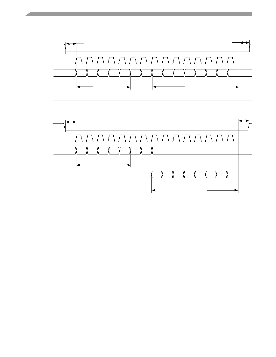
i.MX31/i.MX31L Advance Information, Rev. 1.4
126
Freescale Semiconductor
Preliminary
Electrical Characteristics
Figure 64. 4-wire Serial Interface Timing Diagram
Figure 65
depicts timing of the 5-wire serial interface (Type 1). For this interface, a separate RS line is
added. When a burst is transmitted within single active chip select interval, the RS can be changed at
boundaries of words.
Preamble
DISPB_D#_CS
DISPB_SD_D_CLK
DISPB_SD_D
RW
RS
Output data
D7
D6
D5
D4
D3
D2
D1
D0
DISPB_SD_D
(Output)
(Input)
Preamble
DISPB_D#_CS
DISPB_SD_D_CLK
DISPB_SD_D
RW
RS
Input data
DISPB_SD_D
D7
D6
D5
D4
D3
D2
D1
D0
(Output)
(Input)
Write
Read
1 display IF
clock cycle
1 display IF
clock cycle
1 display IF
clock cycle
1 display IF
clock cycle
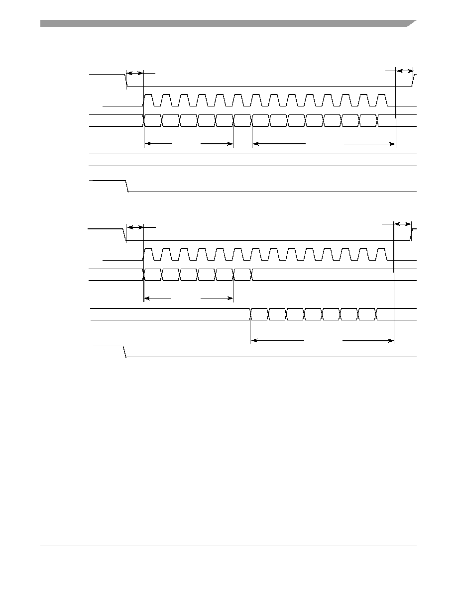
Electrical Characteristics
i.MX31/i.MX31L Advance Information, Rev. 1.4
Freescale Semiconductor
127
Preliminary
Figure 65. 5-wire Serial Interface (Type 1) Timing Diagram
Preamble
DISPB_D#_CS
DISPB_SD_D_CLK
DISPB_SD_D
RW
D7
D6
D5
D4
D3
D2
D1
D0
DISPB_SD_D
(Output)
(Input)
DISPB_D#_CS
DISPB_SD_D_CLK
DISPB_SD_D
RW
DISPB_SD_D
D7
D6
D5
D4
D3
D2
D1
D0
(Output)
(Input)
Write
Read
DISPB_SER_RS
DISPB_SER_RS
1 display IF
clock cycle
1 display IF
clock cycle
Output data
1 display IF
clock cycle
1 display IF
clock cycle
Preamble
Input data
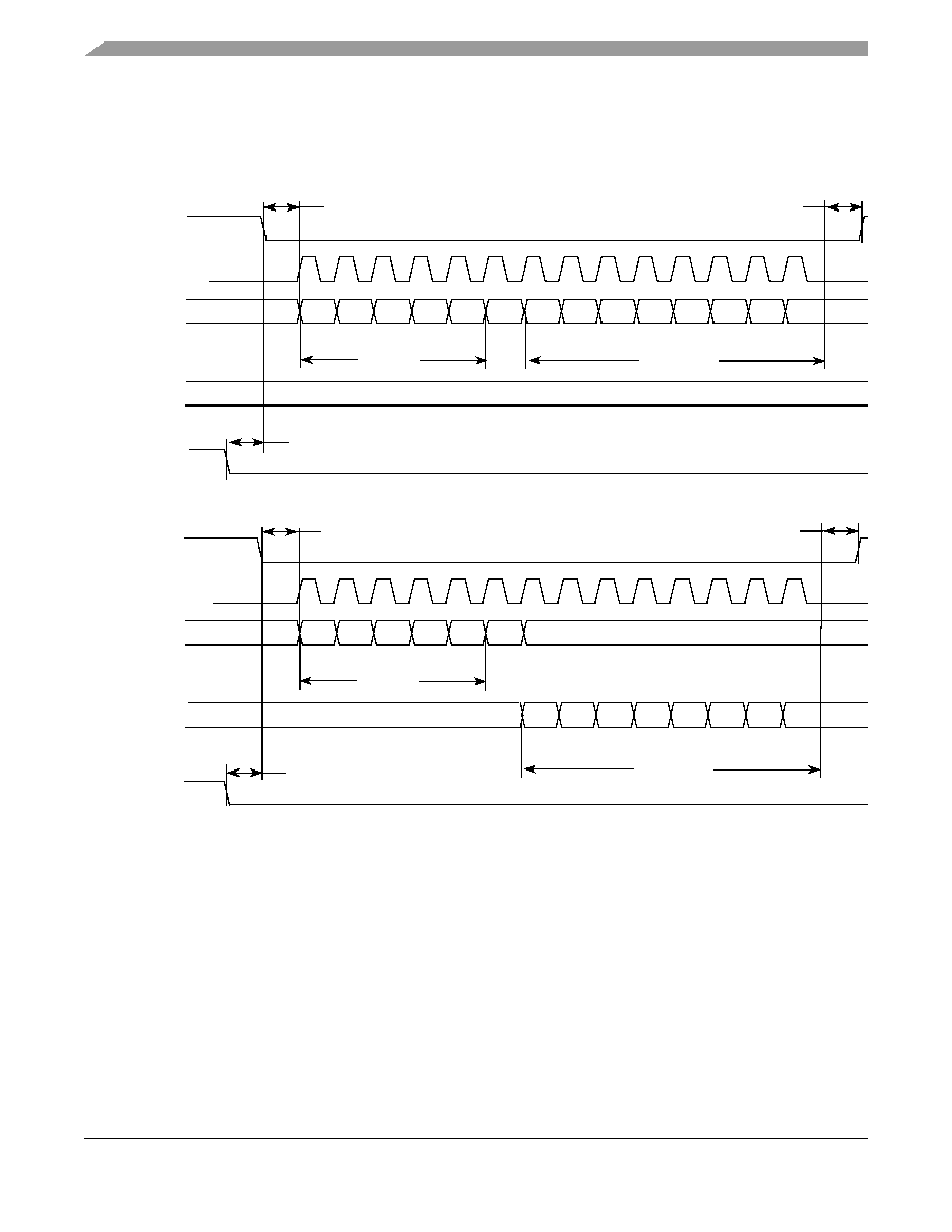
i.MX31/i.MX31L Advance Information, Rev. 1.4
128
Freescale Semiconductor
Preliminary
Electrical Characteristics
Figure 66
depicts timing of the 5-wire serial interface (Type 2). For this interface, a separate RS line is
added. When a burst is transmitted within single active chip select interval, the RS can be changed at
boundaries of words.
Figure 66. 5-wire Serial Interface (Type 2) Timing Diagram
Preamble
DISPB_D#_CS
DISPB_SD_D_CLK
DISPB_SD_D
RW
Output data
D7
D6
D5
D4
D3
D2
D1
D0
DISPB_SD_D
(Output)
(Input)
Preamble
DISPB_D#_CS
DISPB_SD_D_CLK
DISPB_SD_D
RW
Input data
DISPB_SD_D
D7
D6
D5
D4
D3
D2
D1
D0
(Output)
(Input)
Write
Read
DISPB_SER_RS
DISPB_SER_RS
1 display IF
clock cycle
1 display IF
clock cycle
1 display IF
clock cycle
1 display IF
clock cycle
1 display IF
clock cycle
1 display IF
clock cycle
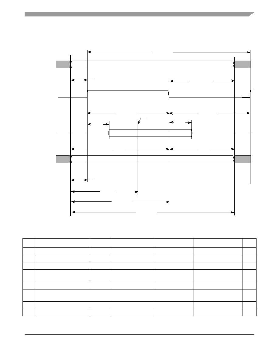
Electrical Characteristics
i.MX31/i.MX31L Advance Information, Rev. 1.4
Freescale Semiconductor
129
Preliminary
4.3.15.5.4
Serial Interfaces,
Electrical Characteristics
Figure 67
depicts timing of the serial interface.
Table 52
lists the timing parameters at display access level.
Figure 67. Asynchronous Serial Interface Timing Diagram
Table 52. Asynchronous Serial Interface Timing Parameters--Access Level
ID
Parameter
Symbol
Min.
Typ.
1
Max.
Units
IP48 Read system cycle time
Tcycr
Tdicpr-1.5
Tdicpr
2
Tdicpr+1.5
ns
IP49 Write system cycle time
Tcycw
Tdicpw-1.5
Tdicpw
3
Tdicpw+1.5
ns
IP50 Read clock low pulse width
Trl
Tdicdr-Tdicur-1.5
Tdicdr
4
-Tdicur
5
Tdicdr-Tdicur+1.5
ns
IP51 Read clock high pulse width
Trh
Tdicpr-Tdicdr+Tdicur-
1.5
Tdicpr-Tdicdr+
Tdicur
Tdicpr-Tdicdr+Tdicur+1.5
ns
IP52 Write clock low pulse width
Twl
Tdicdw-Tdicuw-1.5
Tdicdw
6
-Tdicuw
7
Tdicdw-Tdicuw+1.5
ns
IP53 Write clock high pulse width
Twh
Tdicpw-Tdicdw+
Tdicuw-1.5
Tdicpw-Tdicdw+
Tdicuw
Tdicpw-Tdicdw+
Tdicuw+1.5
ns
IP54 Controls setup time for read
Tdcsr
Tdicur-1.5
Tdicur
≠
ns
IP55 Controls hold time for read
Tdchr
Tdicpr-Tdicdr-1.5
Tdicpr-Tdicdr
≠
ns
IP49, IP48
Read Data
IP51, IP53
IP58
IP59
DISPB_SER_RS
DISPB_DATA
DISPB_DATA
(Input)
(Output)
IP56,IP54
IP57, IP55
IP50, IP52
IP61
IP60
IP67,IP65
IP47
IP64, IP66
IP62, IP63
DISPB_SD_D_CLK
read point
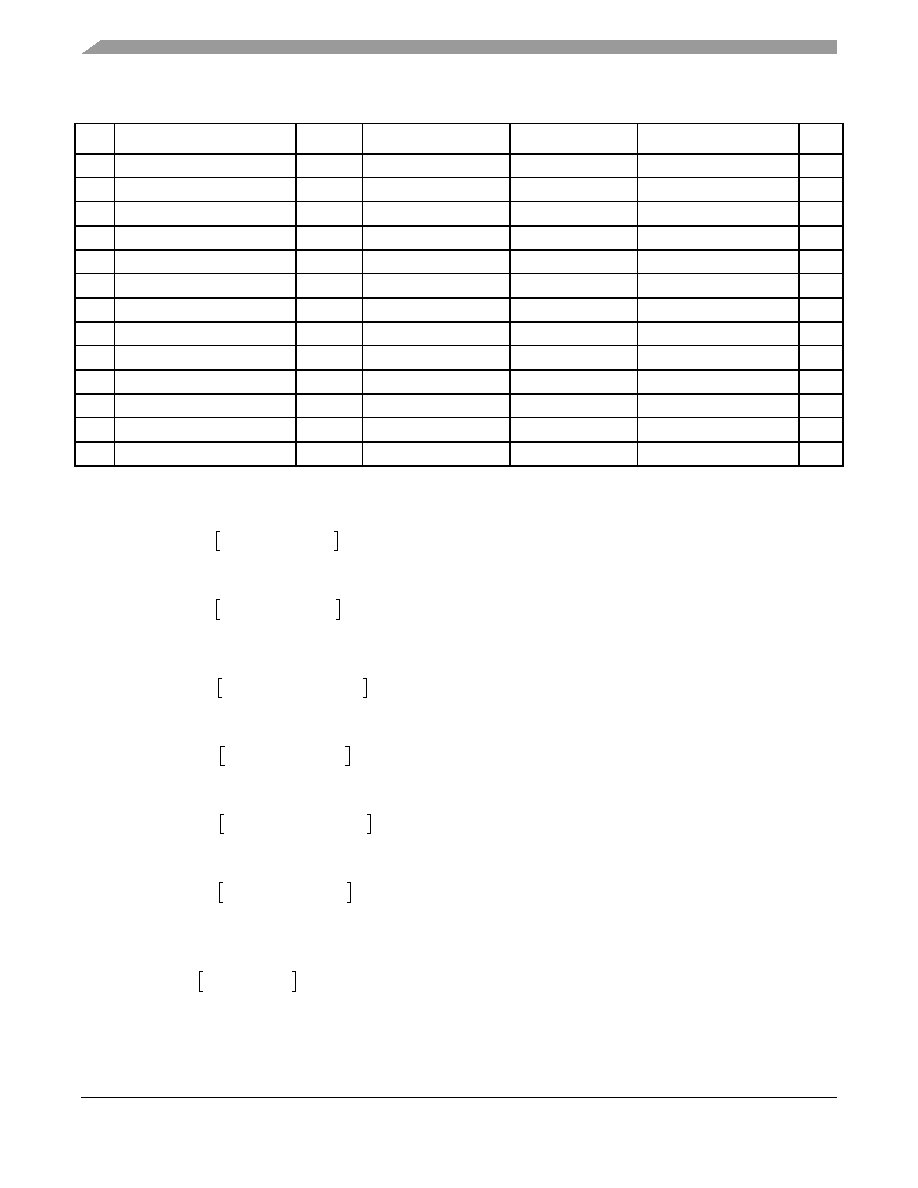
i.MX31/i.MX31L Advance Information, Rev. 1.4
130
Freescale Semiconductor
Preliminary
Electrical Characteristics
IP56 Controls setup time for write
Tdcsw
Tdicuw-1.5
Tdicuw
≠
ns
IP57 Controls hold time for write
Tdchw
Tdicpw-Tdicdw-1.5
Tdicpw-Tdicdw
≠
ns
IP58 Slave device data delay
8
Tracc
0
≠
Tdrp
9
-Tlbd
10
-Tdicur-1.5
ns
IP59 Slave device data hold time
8
Troh
Tdrp-Tlbd-Tdicdr+1.5
≠
Tdicpr-Tdicdr-1.5
ns
IP60 Write data setup time
Tds
Tdicdw-1.5
Tdicdw
≠
ns
IP61 Write data hold time
Tdh
Tdicpw-Tdicdw-1.5
Tdicpw-Tdicdw
≠
ns
IP62 Read period
2
Tdicpr
Tdicpr-1.5
Tdicpr
Tdicpr+1.5
ns
IP63 Write period
3
Tdicpw
Tdicpw-1.5
Tdicpw
Tdicpw+1.5
ns
IP64 Read down time
4
Tdicdr
Tdicdr-1.5
Tdicdr
Tdicdr+1.5
ns
IP65 Read up time
5
Tdicur
Tdicur-1.5
Tdicur
Tdicur+1.5
ns
IP66 Write down time
6
Tdicdw
Tdicdw-1.5
Tdicdw
Tdicdw+1.5
ns
IP67 Write up time
7
Tdicuw
Tdicuw-1.5
Tdicuw
Tdicuw+1.5
ns
IP68 Read time point
9
Tdrp
Tdrp-1.5
Tdrp
Tdrp+1.5
ns
1
The exact conditions have not been finalized, but will likely match the current customer requirement for their specific display. These
conditions may be chip specific.
2
Display interface clock period value for read:
3
Display interface clock period value for write:
4
Display interface clock down time for read:
5
Display interface clock up time for read:
6
Display interface clock down time for write:
7
Display interface clock up time for write:
8
This parameter is a requirement to the display connected to the IPU.
9
Data read point:
10
Loopback delay Tlbd is the cumulative propagation delay of read controls and read data. It includes an IPU output delay, a
chip-level output delay, board delays, a chip-level input delay, an IPU input delay. This value is chip specific.
Table 52. Asynchronous Serial Interface Timing Parameters--Access Level (continued)
ID
Parameter
Symbol
Min.
Typ.
1
Max.
Units
Tdicpr
THSP_CLK ceil
DISP#_IF_CLK_PER_RD
HSP_CLK_PERIOD
----------------------------------------------------------------
=
Tdicpw
THSP_CLK ceil
DISP#_IF_CLK_PER_WR
HSP_CLK_PERIOD
------------------------------------------------------------------
=
Tdicdr
1
2
---
THSP_CLK ceil
2 DISP#_IF_CLK_DOWN_RD
HSP_CLK_PERIOD
-------------------------------------------------------------------------------
=
Tdicur
1
2
---
THSP_CLK ceil
2 DISP#_IF_CLK_UP_RD
HSP_CLK_PERIOD
--------------------------------------------------------------------
=
Tdicdw
1
2
---
THSP_CLK ceil
2 DISP#_IF_CLK_DOWN_WR
HSP_CLK_PERIOD
---------------------------------------------------------------------------------
=
Tdicuw
1
2
---
THSP_CLK ceil
2 DISP#_IF_CLK_UP_WR
HSP_CLK_PERIOD
----------------------------------------------------------------------
=
Tdrp
THSP_CLK ceil
DISP#_READ_EN
HSP_CLK_PERIOD
--------------------------------------------------
=
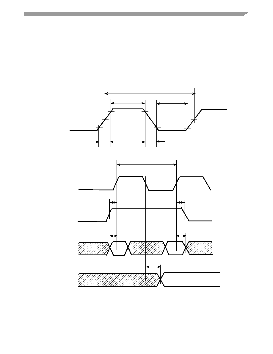
Electrical Characteristics
i.MX31/i.MX31L Advance Information, Rev. 1.4
Freescale Semiconductor
131
Preliminary
The DISP#_IF_CLK_PER_WR, DISP#_IF_CLK_PER_RD, HSP_CLK_PERIOD,
DISP#_IF_CLK_DOWN_WR, DISP#_IF_CLK_UP_WR, DISP#_IF_CLK_DOWN_RD,
DISP#_IF_CLK_UP_RD and DISP#_READ_EN parameters are programmed via the
DI_DISP#_TIME_CONF_1, DI_DISP#_TIME_CONF_2 and DI_HSP_CLK_PER Registers.
4.3.16
Memory Stick Host Controller (MSHC)
Figure 68
,
Figure 69
, and
Figure 70
depict the MSHC timings, and
Table 53
and
Table 54
list the timing
parameters.
Figure 68. MSHC_CLK Timing Diagram
Figure 69. Transfer Operation Timing Diagram (Serial)
tSCLKwh
tSCLKwl
tSCLKc
tSCLKr
tSCLKf
MSHC_SCLK
tSCLKc
MSHC_SCLK
tBSsu
tBSh
tDsu
tDh
MSHC_BS
MSHC_DATA
(Output)
tDd
MSHC_DATA
(Intput)
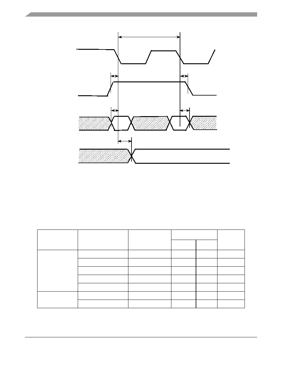
i.MX31/i.MX31L Advance Information, Rev. 1.4
132
Freescale Semiconductor
Preliminary
Electrical Characteristics
Figure 70. Transfer Operation Timing Diagram (Parallel)
NOTE
The Memory Stick Host Controller is designed to meet the timing
requirements per Sony's Memory Stick Pro Format Specifications document.
Tables in this section details the specifications requirements for parallel and
serial modes, and not the i.MX31/i.MX31L timing. The timing will be
provided once IC characterization is complete.
Table 53. Serial Interface Timing Parameters
Signal
Parameter
Symbol
Standards
Unit
Min.
Max.
MSHC_SCLK
Cycle
tSCLKc
50
≠
ns
H pulse length
tSCLKwh
15
≠
ns
L pulse length
tSCLKwl
15
≠
ns
Rise time
tSCLKr
≠
10
ns
Fall time
tSCLKf
≠
10
ns
MSHC_BS
Setup time
tBSsu
5
≠
ns
Hold time
tBSh
5
≠
ns
tSCLKc
MSHC_SCLK
tBSsu
tBSh
tDsu
tDh
MSHC_BS
MSHC_DATA
(Output)
tDd
MSHC_DATA
(Intput)
Electrical Characteristics
i.MX31/i.MX31L Advance Information, Rev. 1.4
Freescale Semiconductor
133
Preliminary
4.3.17
Personal Computer Memory Card International Association
(PCMCIA)
Figure 71
and
Figure 72
depict the timings pertaining to the PCMCIA module, each of which is an
example of one clock of strobe set-up time and one clock of strobe hold time.
Table 55
lists the timing
parameters.
MSHC_DATA
Setup time
tDsu
5
≠
ns
Hold time
tDh
5
≠
ns
Output delay time
tDd
≠
15
ns
Table 54. Parallel Interface Timing Parameters
Signal
Parameter
Symbol
Standards
Unit
Min
Max
MSHC_SCLK
Cycle
tSCLKc
25
≠
ns
H pulse length
tSCLKwh
5
≠
ns
L pulse length
tSCLKwl
5
≠
ns
Rise time
tSCLKr
≠
10
ns
Fall time
tSCLKf
≠
10
ns
MSHC_BS
Setup time
tBSsu
8
≠
ns
Hold time
tBSh
1
≠
ns
MSHC_DATA
Setup time
tDsu
8
≠
ns
Hold time
tDh
1
≠
ns
Output delay time
tDd
≠
15
ns
Table 53. Serial Interface Timing Parameters (continued)
Signal
Parameter
Symbol
Standards
Unit
Min.
Max.
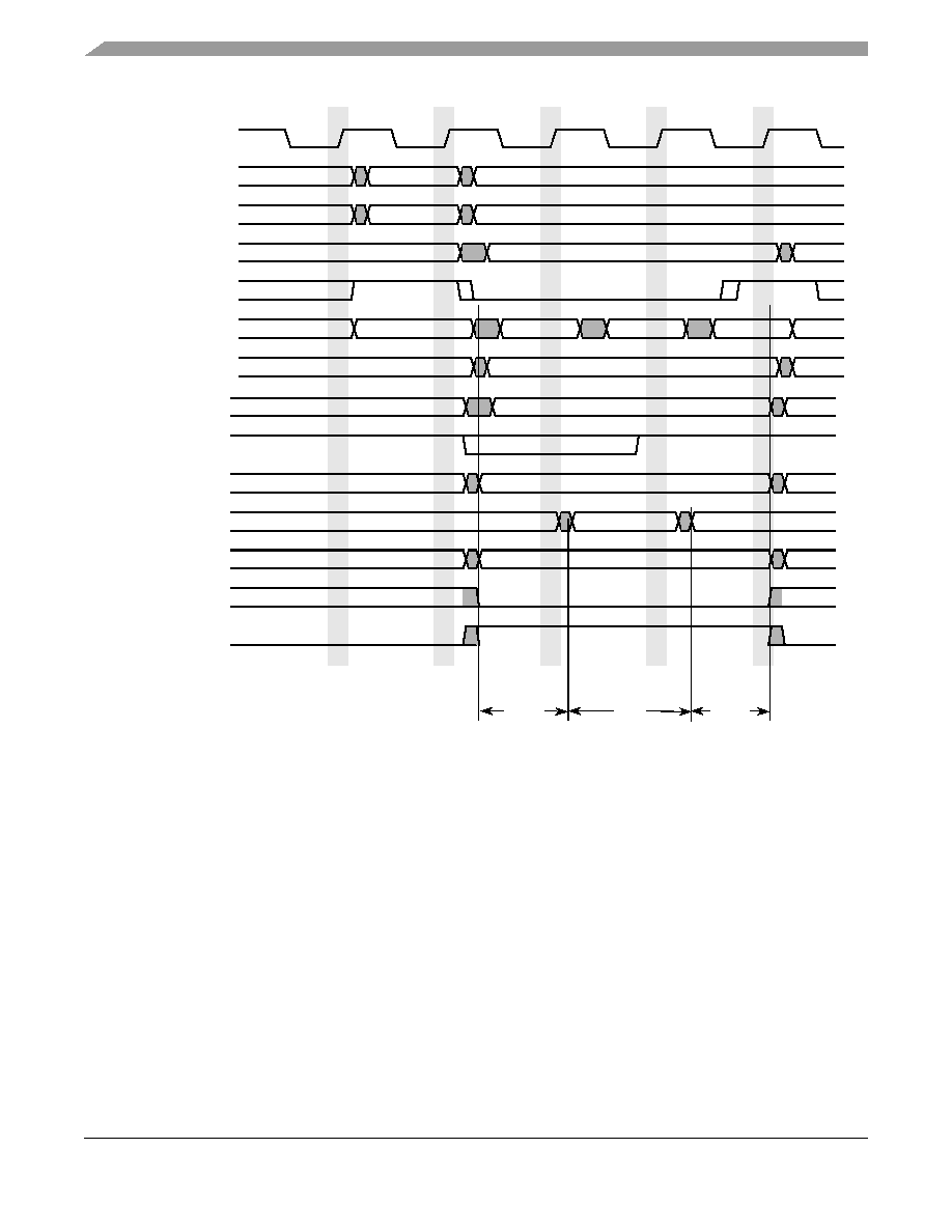
i.MX31/i.MX31L Advance Information, Rev. 1.4
134
Freescale Semiconductor
Preliminary
Electrical Characteristics
Figure 71. Write Accesses Timing Diagram--PSHT=1, PSST=1
HCLK
HADDR
ADDR 1
CONTROL
CONTROL 1
HWDATA
DATA write 1
HREADY
HRESP
OKAY
OKAY
OKAY
A[25:0]
ADDR 1
D[15:0]
DATA write 1
WAIT
REG
REG
OE/WE/IORD/IOWR
CE1/CE2
RD/WR
POE
PSST
PSHT
PSL
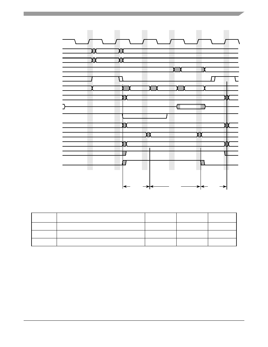
Electrical Characteristics
i.MX31/i.MX31L Advance Information, Rev. 1.4
Freescale Semiconductor
135
Preliminary
Figure 72. Read Accesses Timing Diagram--PSHT=1, PSST=1
4.3.18
PWM Electrical Specifications
This section describes the electrical information of the PWM. The PWM can be programmed to select one
of three clock signals as its source frequency. The selected clock signal is passed through a prescaler before
being input to the counter. The output is available at the pulse-width modulator output (PWMO) external
pin.
Table 55. PCMCIA Write and Read Timing Parameters
Symbol
Parameter
Min
Max
Unit
PSHT
PCMCIA strobe hold time
0
63
clock
PSST
PCMCIA strobe set up time
1
63
clock
PSL
PCMCIA strobe length
1
128
clock
HCLK
HADDR
ADDR 1
CONTROL
CONTROL 1
RWDATA
DATA read 1
HREADY
HRESP
OKAY
OKAY
OKAY
A[25:0]
ADDR 1
D[15:0]
WAIT
REG
REG
OE/WE/IORD/IOWR
CE1/CE2
RD/WR
POE
PSST
PSHT
PSL
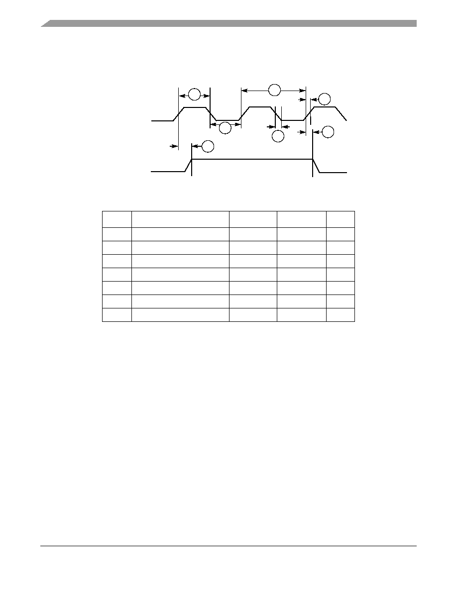
i.MX31/i.MX31L Advance Information, Rev. 1.4
136
Freescale Semiconductor
Preliminary
Electrical Characteristics
4.3.18.1
PWM Timing
Figure 73
depicts the timing of the PWM, and
Table 56
lists the PWM timing characteristics.
Figure 73. PWM Timing
Table 56. PWM Output Timing Parameters
ID
Parameter
Min
Max
Unit
1
System CLK frequency
1
1
CL of PWMO = 30 pF
0
ipg_clk
MHz
2a
Clock high time
12.29
≠
ns
2b
Clock low time
9.91
≠
ns
3a
Clock fall time
≠
0.5
ns
3b
Clock rise time
≠
0.5
ns
4a
Output delay time
≠
9.37
ns
4b
Output setup time
8.71
≠
ns
System Clock
2a
1
PWM Output
3b
2b
3a
4b
4a
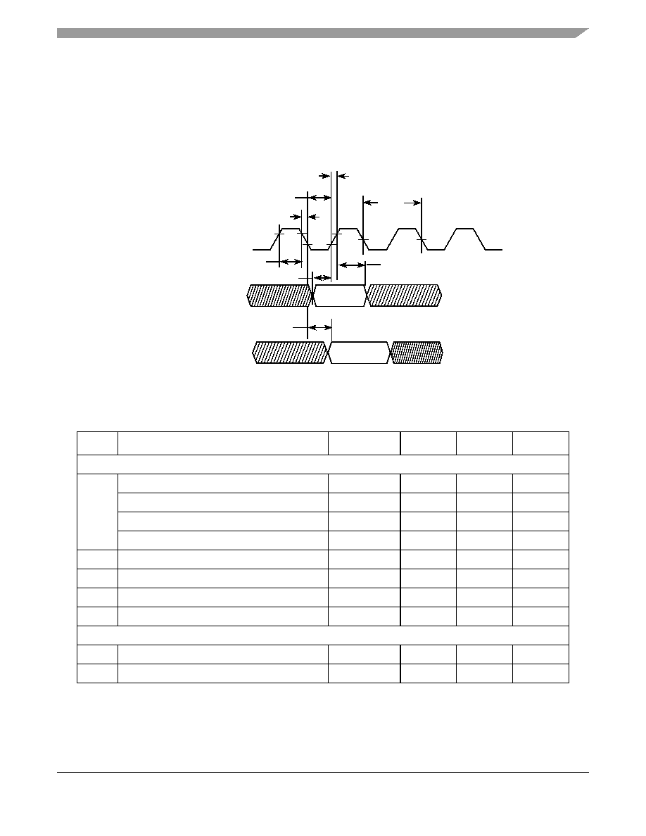
Electrical Characteristics
i.MX31/i.MX31L Advance Information, Rev. 1.4
Freescale Semiconductor
137
Preliminary
4.3.19
SDHC Electrical Specifications
This section describes the electrical information of the SDHC.
4.3.19.1
SDHC Timing
Figure 74
depicts the timings of the SDHC, and
Table 57
lists the timing parameters.
Figure 74. SDHC Timing Diagram
.
Table 57. SDHC Interface Timing Parameters
ID
Parameter
Symbol
Min
Max
Unit
Card Input Clock
SD1
Clock Frequency (Low Speed)
f
PP
1
0
400
kHz
Clock Frequency (SD/SDIO Full Speed)
f
PP
2
0
25
MHz
Clock Frequency (MMC Full Speed)
f
PP
3
0
20
MHz
Clock Frequency (Identification Mode)
f
OD
4
100
400
kHz
SD2
Clock Low Time
t
WL
10
≠
ns
SD3
Clock High Time
t
WH
10
≠
ns
SD4
Clock Rise Time
t
TLH
≠
10
ns
SD5
Clock Fall Time
t
THL
≠
10
ns
SDHC output / Card Inputs CMD, DAT (Reference to CLK)
SD6
SDHC output / Card input Set-up Time
t
ISU
5
≠
ns
SD7
SDHC output / Card input Hold Time
t
IH
5
≠
ns
SD1
SD3
SD5
SD7
SD4
SD8
MMCx_CLK
MMCx_CMD
output from SDHC to card
MMCx_DAT_1
MMCx_DAT_2
MMCx_DAT_3
MMCx_DAT_0
MMCx_CMD
input from card to SDHC
MMCx_DAT_1
MMCx_DAT_2
MMCx_DAT_3
MMCx_DAT_0
MMCx_CLK
SD2
SD6
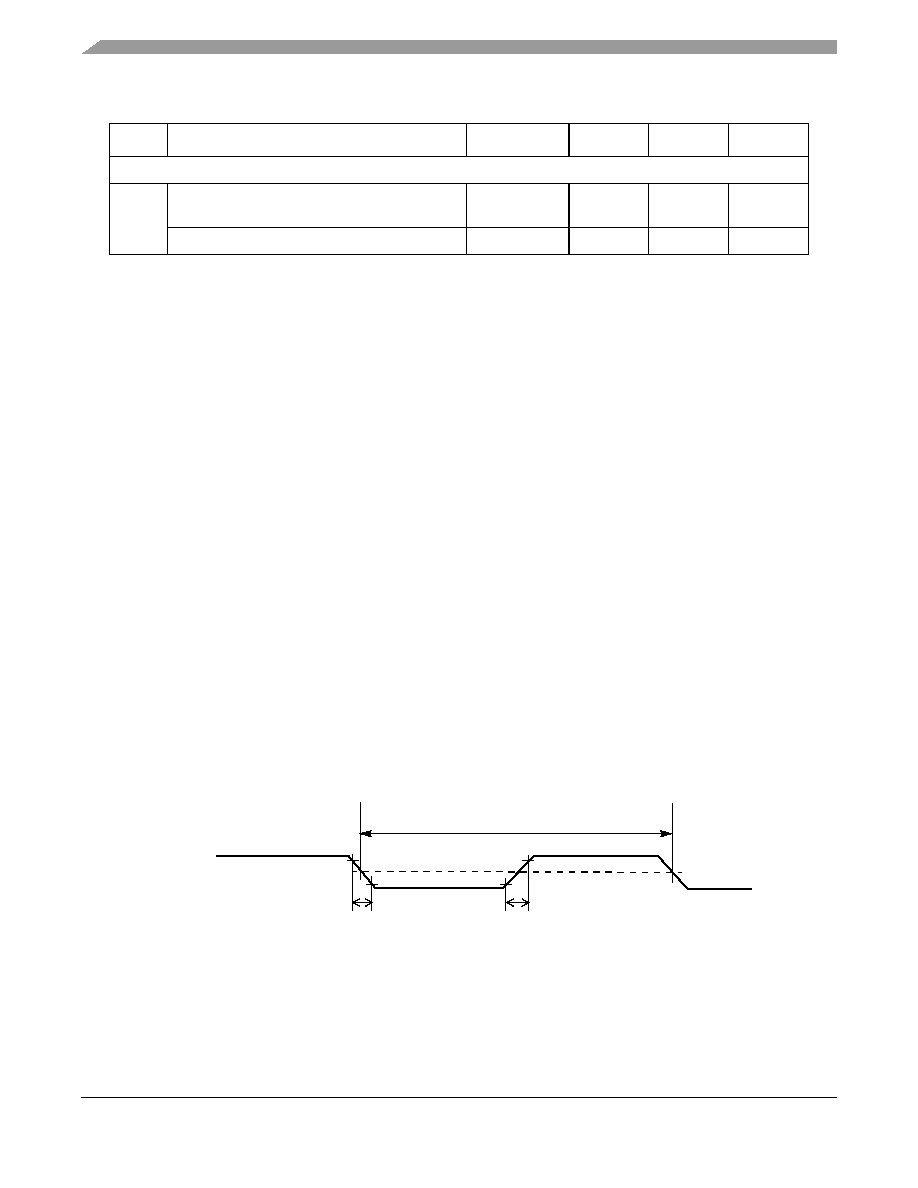
i.MX31/i.MX31L Advance Information, Rev. 1.4
138
Freescale Semiconductor
Preliminary
Electrical Characteristics
4.3.20
SIM Electrical Specifications
Each SIM card interface consist of a total of 12 pins (for 2 separate ports of 6 pins each. Mostly one port
with 5 pins is used).
The interface is meant to be used with synchronous SIM cards. This means that the SIM module provides
a clock for the SIM card to use. The frequency of this clock is normally 372 times the data rate on the
TX/RX pins, however SIM module can work with CLK equal to 16 times the data rate on TX/RX pins.
There is no timing relationship between the clock and the data. The clock that the SIM module provides
to the aim card will be used by the SIM card to recover the clock from the data much like a standard UART.
All six (or 5 in case bi directional TXRX is used) of the pins for each half of the SIM module are
asynchronous to each other.
There are no required timing relationships between the pads in normal mode, but there are some in two
specific cases: reset and power down sequences.
4.3.20.1
General Timing Requirements
Figure 75
shows the timing of the SIM module, and
Figure 58
lists the timing parameters.
Figure 75. SIM Clock Timing Diagram
SDHC input / Card Outputs CMD, DAT (Reference to CLK)
SD8
Card Output Delay Time during Data Transfer
Mode
t
ODLY
5
0
14
ns
Output Delay time during Identification Mode
t
ODLY
6
0
50
ns
1
In low speed mode, card clock must be lower than 400 kHz, voltage ranges from 2.7 to 3.6 V.
2
In normal data transfer mode for SD/SDIO card, clock frequency can be any value between 0 ~ 25 MHz.
3
In normal data transfer mode for MMC card, clock frequency can be any value between 0 ~ 20 MHz.
4
In card identification mode, card clock must be l100 kHz ~ 400 kHz, voltage ranges from 2.7 to 3.6 V.
5
In identification mode, card output delay time should be less than 50 ns.
6
In data transfer mode, card output delay time should be less than 14 ns.
Table 57. SDHC Interface Timing Parameters (continued)
ID
Parameter
Symbol
Min
Max
Unit
CLK
Srise
Sfall
1/Sfreq
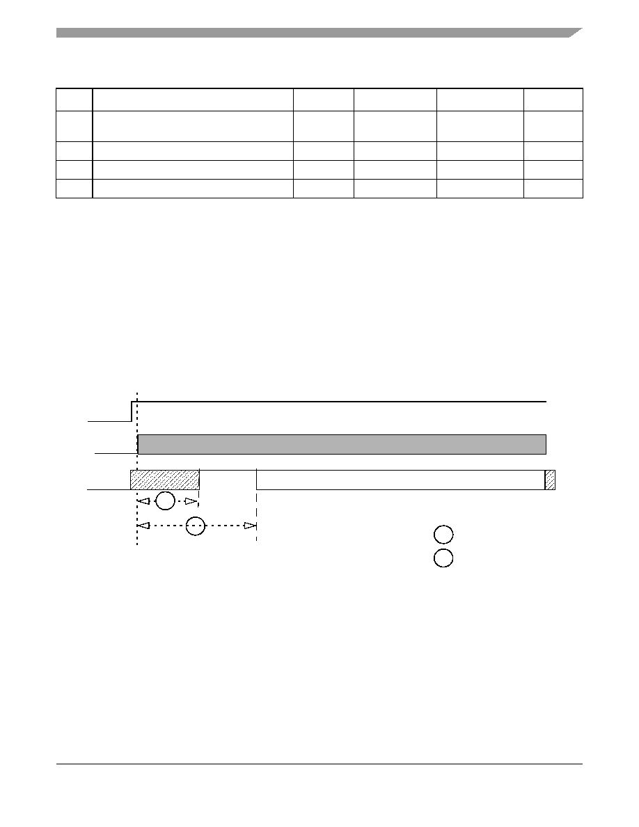
Electrical Characteristics
i.MX31/i.MX31L Advance Information, Rev. 1.4
Freescale Semiconductor
139
Preliminary
4.3.20.2
Reset Sequence
4.3.20.2.1
Cards with Internal Reset
The sequence of reset for this kind of SIM Cards is as follows (see
Figure 76
):
∑
After powerup, the clock signal is enabled on SGCLK (time T0)
∑
After 200 clock cycles, RX must be high.
∑
The card must send a response on RX acknowledging the reset between 400 and 40000 clock cycles
after T0.
Figure 76. Internal-Reset Card Reset Sequence
4.3.20.2.2
Cards with Active Low Reset
The sequence of reset for this kind of card is as follows (see
Figure 77
):
1. After powerup, the clock signal is enabled on CLK (time T0)
2. After 200 clock cycles, RX must be high.
3. RST must remain Low for at least 40000 clock cycles after T0 (no response is to be received on
RX during those 40000 clock cycles)
4. RST is set High (time T1)
Table 58. SIM Timing Specification--High Drive Strength
Num
Description
Symbol
Min
Max
Unit
1
SIM Clock Frequency (CLK)
1
1
50% duty cycle clock
S
freq
0.01
5 (Some new cards
may reach 10)
MHz
2
SIM CLK Rise Time
2
2
With C = 50pF
S
rise
≠
20
ns
3
SIM CLK Fall Time
3
3
With C = 50pF
S
fall
≠
20
ns
4
SIM Input Transition Time (RX, SIMPD)
S
trans
≠
25
ns
SVEN
CLK
RX
2
T0
1
response
2
1
< 200 clock cycles
< 40000 clock cycles
400 clock cycles <
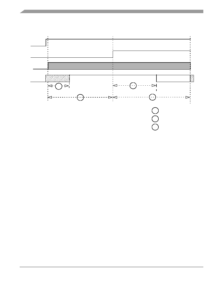
i.MX31/i.MX31L Advance Information, Rev. 1.4
140
Freescale Semiconductor
Preliminary
Electrical Characteristics
5. RST must remain High for at least 40000 clock cycles after T1 and a response must be received
on RX between 400 and 40000 clock cycles after T1.
Figure 77. Active-Low-Reset Card Reset Sequence
4.3.20.3
Power Down Sequence
Power down sequence for SIM interface is as follows:
1. SIMPD port detects the removal of the SIM Card
2. RST goes Low
3. CLK goes Low
4. TX goes Low
5. VEN goes Low
Each of this steps is done in one CKIL period (usually 32 kHz). Power down can be started because of a
SIM Card removal detection or launched by the processor.
Figure 78
and
Table 59
show the usual timing
requirements for this sequence, with Fckil = CKIL frequency value.
SVEN
CLK
RX
2
T0
1
response
RST
T1
1
2
< 200 clock cycles
< 40000 clock cycles
400 clock cycles <
3
3
3
400000 clock cycles <
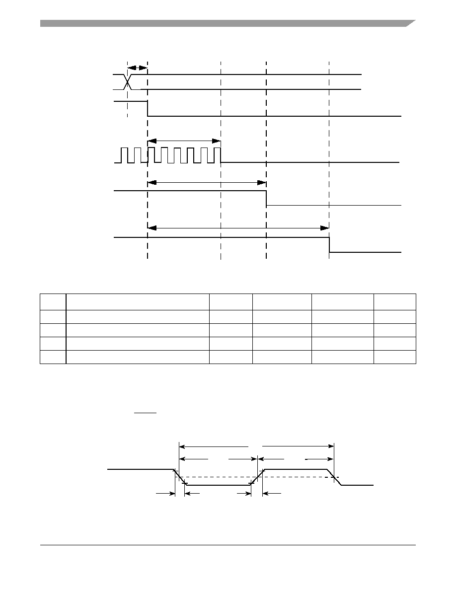
Electrical Characteristics
i.MX31/i.MX31L Advance Information, Rev. 1.4
Freescale Semiconductor
141
Preliminary
Figure 78. SmartCard Interface Power Down AC Timing
4.3.21
SJC Electrical Specifications
This section details the electrical characteristics for the SJC module.
Figure 79
depicts the SJC test clock
input timing.
Figure 80
depicts the SJC boundary scan timing,
Figure 81
depicts the SJC test access port,
Figure 82
depicts the SJC TRST timing, and
Table 60
lists the SJC timing parameters.
Figure 79. Test Clock Input Timing Diagram
Table 59. Timing Requirements for Power Down Sequence
Num
Description
Symbol
Min
Max
Unit
1
SIM reset to SIM clock stop
S
rst2clk
0.9*1/FCKIL
0.8
µs
2
SIM reset to SIM TX data low
S
rst2dat
1.8*1/FCKIL
1.2
µs
3
SIM reset to SIM Voltage Enable Low
S
rst2ven
2.7*1/FCKIL
1.8
µs
4
SIM Presence Detect to SIM reset Low
S
pd2rst
0.9*1/FCKIL
25
ns
SIMPD
RST
CLK
DATA_TX
SVEN
Srst2clk
Srst2dat
Srst2ven
Spd2rst
TCK
(Input)
VM
VM
VIH
VIL
SJ1
SJ2
SJ2
SJ3
SJ3
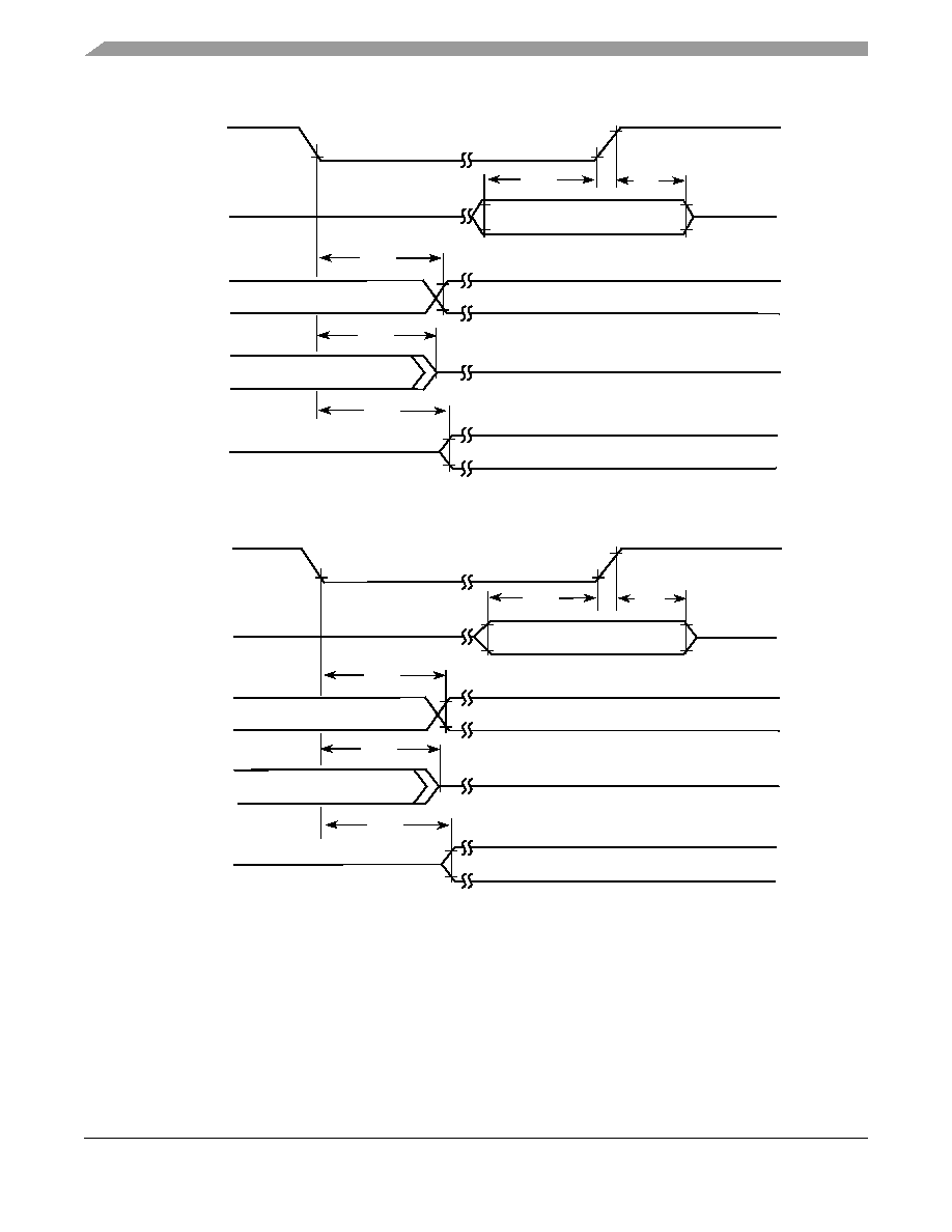
i.MX31/i.MX31L Advance Information, Rev. 1.4
142
Freescale Semiconductor
Preliminary
Electrical Characteristics
Figure 80. Boundary Scan (JTAG) Timing Diagram
Figure 81. Test Access Port Timing Diagram
TCK
(Input)
Data
Inputs
Data
Outputs
Data
Outputs
Data
Outputs
VIH
VIL
Input Data Valid
Output Data Valid
Output Data Valid
SJ4
SJ5
SJ6
SJ7
SJ6
TCK
(Input)
TDI
(Input)
TDO
(Output)
TDO
(Output)
TDO
(Output)
VIH
VIL
Input Data Valid
Output Data Valid
Output Data Valid
TMS
SJ8
SJ9
SJ10
SJ11
SJ10
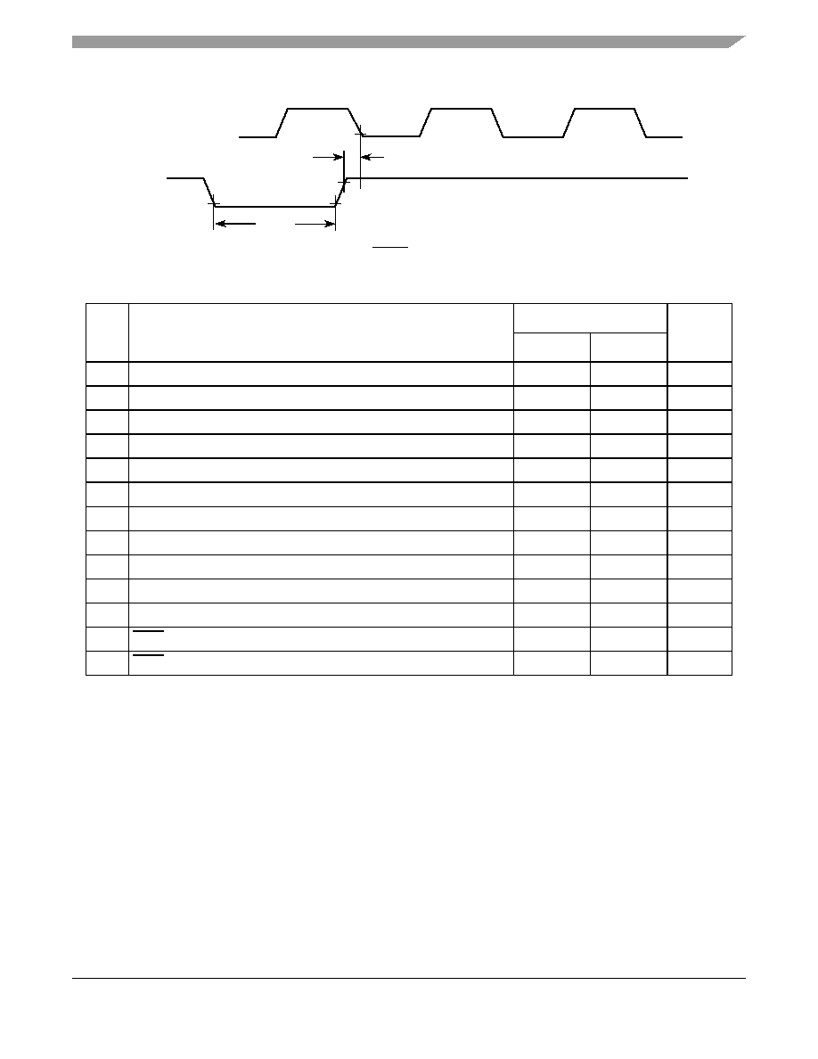
Electrical Characteristics
i.MX31/i.MX31L Advance Information, Rev. 1.4
Freescale Semiconductor
143
Preliminary
Figure 82. TRST Timing Diagram
4.3.22
SSI Electrical Specifications
This section describes the electrical information of SSI.
4.3.22.1
SSI Transmitter Timing with Internal Clock
Figure 83
depicts the SSI transmitter timing with internal clock, and
Table 61
lists the timing parameters.
Table 60. SJC Timing Parameters
ID
Parameter
1
All Frequencies
Unit
Min Max
SJ1
TCK cycle time
100.0
≠
ns
SJ2
TCK clock pulse width measured at
V
M
1
1
V
M -
mid point voltage
40.0
≠
ns
SJ3
TCK rise and fall times
≠
3.0
ns
SJ4
Boundary scan input data set-up time
10.0
≠
ns
SJ5
Boundary scan input data hold time
50.0
≠
ns
SJ6
TCK low to output data valid
≠
40.0
ns
SJ7
TCK low to output high impedance
≠
40.0
ns
SJ8
TMS, TDI data set-up time
10.0
≠
ns
SJ9
TMS, TDI data hold time
50.0
≠
ns
SJ10
TCK low to TDO data valid
≠
44.0
ns
SJ11
TCK low to TDO high impedance
≠
44.0
ns
SJ12
TRST assert time
100.0
≠
ns
SJ13
TRST set-up time to TCK low
40.0
≠
ns
TCK
(Input)
TRST
(Input)
SJ13
SJ12
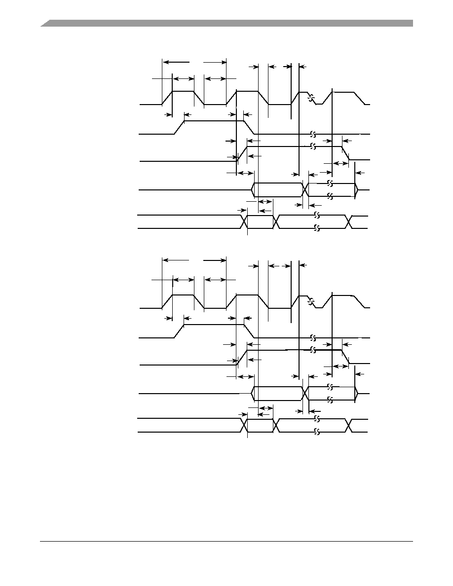
i.MX31/i.MX31L Advance Information, Rev. 1.4
144
Freescale Semiconductor
Preliminary
Electrical Characteristics
Figure 83. SSI Transmitter with Internal Clock Timing Diagram
SS19
AD1_TXC
AD1_TXFS (bl)
AD1_TXFS (wl)
SS1
AD1_TXD
AD1_RXD
SS2
SS4
SS3
SS5
SS6
SS8
SS10
SS12
SS14
SS18
SS15
SS17
SS16
SS43
SS42
Note: SRXD Input in Synchronous mode only
(Output)
(Output)
(Output)
(Output)
(Input)
SS19
DAM1_T_CLK
DAM1_T_FS (bl)
DAM1_T_FS (wl)
SS1
DAM1_TXD
DAM1_RXD
SS2
SS4
SS3
SS5
SS6
SS8
SS10
SS12
SS14
SS18
SS15
SS17
SS16
SS42
Note: SRXD Input in Synchronous mode only
(Output)
(Output)
(Output)
(Output)
(Input)
SS43
Electrical Characteristics
i.MX31/i.MX31L Advance Information, Rev. 1.4
Freescale Semiconductor
145
Preliminary
∑
All the timings for the SSI are given for a non-inverted serial clock polarity (TSCKP/RSCKP = 0)
and a non-inverted frame sync (TFSI/RFSI = 0). If the polarity of the clock and/or the frame sync
have been inverted, all the timing remains valid by inverting the clock signal STCK/SRCK and/or
the frame sync STFS/SRFS shown in the tables and in the figures.
∑
All timings are on AUDMUX pads when SSI is being used for data transfer.
∑
"Tx" and "Rx" refer to the Transmit and Receive sections of the SSI.
∑
For internal Frame Sync operation using external clock, the FS timing will be same as that of Tx
Data (for example, during AC97 mode of operation).
Table 61. SSI Transmitter with Internal Clock Timing Parameters
ID
Parameter
Min
Max
Unit
Internal Clock Operation
SS1
(Tx/Rx) CK clock period
81.4
≠
ns
SS2
(Tx/Rx) CK clock high period
36.0
≠
ns
SS3
(Tx/Rx) CK clock rise time
≠
6
ns
SS4
(Tx/Rx) CK clock low period
36.0
≠
ns
SS5
(Tx/Rx) CK clock fall time
≠
6
ns
SS6
(Tx) CK high to FS (bl) high
≠
15.0
ns
SS8
(Tx) CK high to FS (bl) low
≠
15.0
ns
SS10
(Tx) CK high to FS (wl) high
≠
15.0
ns
SS12
(Tx) CK high to FS (wl) low
≠
15.0
ns
SS14
(Tx/Rx) Internal FS rise time
≠
6
ns
SS15
(Tx/Rx) Internal FS fall time
≠
6
ns
SS16
(Tx) CK high to STXD valid from high
impedance
≠
15.0
ns
SS17
(Tx) CK high to STXD high/low
≠
15.0
ns
SS18
(Tx) CK high to STXD high impedance
≠
15.0
ns
SS19
STXD rise/fall time
≠
6
ns
Synchronous Internal Clock Operation
SS42
SRXD setup before (Tx) CK falling
10.0
≠
ns
SS43
SRXD hold after (Tx) CK falling
0
≠
ns
SS52
Loading ≠
25
pF
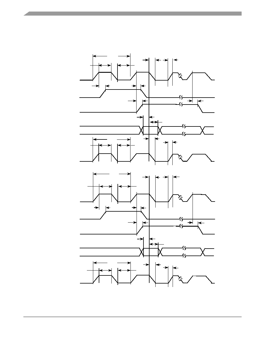
i.MX31/i.MX31L Advance Information, Rev. 1.4
146
Freescale Semiconductor
Preliminary
Electrical Characteristics
4.3.22.2
SSI Receiver Timing with Internal Clock
Figure 84
depicts the SSI receiver timing with internal clock, and
Table 62
lists the timing parameters.
Figure 84. SSI Receiver with Internal Clock Timing Diagram
SS50
SS48
AD1_TXC
AD1_TXFS (bl)
AD1_TXFS (wl)
AD1_RXD
AD1_RXC
SS1
SS4
SS2
SS51
SS20
SS21
SS49
SS7
SS9
SS11
SS13
SS47
(Output)
(Output)
(Output)
(Input)
(Output)
SS3
SS5
SS50
SS48
DAM1_T_CLK
DAM1_T_FS (bl)
DAM1_T_FS (wl)
DAM1_RXD
DAM1_R_CLK
SS3
SS1
SS4
SS2
SS5
SS51
SS20
SS21
SS49
SS7
SS9
SS11
SS13
SS47
(Output)
(Output)
(Output)
(Input)
(Output)
Electrical Characteristics
i.MX31/i.MX31L Advance Information, Rev. 1.4
Freescale Semiconductor
147
Preliminary
NOTE
All the timings for the SSI are given for a non-inverted serial clock polarity
(TSCKP/RSCKP = 0) and a non-inverted frame sync (TFSI/RFSI = 0). If the
polarity of the clock and/or the frame sync have been inverted, all the timing
remains valid by inverting the clock signal STCK/SRCK and/or the frame
sync STFS/SRFS shown in the tables and in the figures.
NOTE
All timings are on AUDMUX pads when SSI is being used for data transfer.
NOTE
"Tx" and "Rx" refer to the Transmit and Receive sections of the SSI.
NOTE
For internal Frame Sync operation using external clock, the FS timing is the
same as that of Tx Data, for example, during the AC97 mode of operation.
Table 62. SSI Receiver with Internal Clock Timing Parameters
ID
Parameter
Min
Max
Unit
Internal Clock Operation
SS1
(Tx/Rx) CK clock period
81.4
≠
ns
SS2
(Tx/Rx) CK clock high period
36.0
≠
ns
SS3
(Tx/Rx) CK clock rise time
≠
6
ns
SS4
(Tx/Rx) CK clock low period
36.0
≠
ns
SS5
(Tx/Rx) CK clock fall time
≠
6
ns
SS7
(Rx) CK high to FS (bl) high
≠
15.0
ns
SS9
(Rx) CK high to FS (bl) low
≠
15.0
ns
SS11
(Rx) CK high to FS (wl) high
≠
15.0
ns
SS13
(Rx) CK high to FS (wl) low
≠
15.0
ns
SS20
SRXD setup time before (Rx) CK low
10.0
≠
ns
SS21
SRXD hold time after (Rx) CK low
0
≠
ns
Oversampling Clock Operation
SS47
Oversampling clock period
15.04
≠
ns
SS48
Oversampling clock high period
6
≠
ns
SS49
Oversampling clock rise time
≠
3
ns
SS50
Oversampling clock low period
6
≠
ns
SS51
Oversampling clock fall time
≠
3
ns
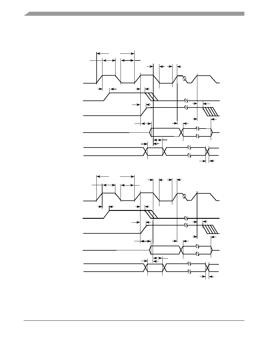
i.MX31/i.MX31L Advance Information, Rev. 1.4
148
Freescale Semiconductor
Preliminary
Electrical Characteristics
4.3.22.3
SSI Transmitter Timing with External Clock
Figure 85
depicts the SSI transmitter timing with external clock, and
Table 63
lists the timing parameters.
Figure 85. SSI Transmitter with External Clock Timing Diagram
SS45
SS33
SS24
SS26
SS25
SS23
AD1_TXC
AD1_TXFS (bl)
AD1_TXFS (wl)
AD1_TXD
AD1_RXD
Note: SRXD Input in Synchronous mode only
SS31
SS29
SS27
SS22
SS44
SS39
SS38
SS37
SS46
(Input)
(Input)
(Input)
(Output)
(Input)
SS45
SS33
SS24
SS26
SS25
SS23
DAM1_T_CLK
DAM1_T_FS (bl)
DAM1_T_FS (wl)
DAM1_TXD
DAM1_RXD
Note: SRXD Input in Synchronous mode only
SS31
SS29
SS27
SS22
SS44
SS39
SS38
SS37
SS46
(Input)
(Input)
(Input)
(Output)
(Input)
Electrical Characteristics
i.MX31/i.MX31L Advance Information, Rev. 1.4
Freescale Semiconductor
149
Preliminary
NOTE
All the timings for the SSI are given for a non-inverted serial clock polarity
(TSCKP/RSCKP = 0) and a non-inverted frame sync (TFSI/RFSI = 0). If the
polarity of the clock and/or the frame sync have been inverted, all the timing
remains valid by inverting the clock signal STCK/SRCK and/or the frame
sync STFS/SRFS shown in the tables and in the figures.
NOTE
All timings are on AUDMUX pads when the SSI is being used for data
transfer.
NOTE
"Tx" and "Rx" refer to the Transmit and Receive sections of the SSI.
NOTE
For internal Frame Sync operation using external clock, the FS timing will
be same as that of Tx Data, for example, during the AC97 mode of
operation.
Table 63. SSI Transmitter with External Clock Timing Parameters
ID
Parameter
Min
Max
Unit
External Clock Operation
SS22
(Tx/Rx) CK clock period
81.4
≠
ns
SS23
(Tx/Rx) CK clock high period
36.0
≠
ns
SS24
(Tx/Rx) CK clock rise time
≠
6.0
ns
SS25
(Tx/Rx) CK clock low period
36.0
≠
ns
SS26
(Tx/Rx) CK clock fall time
≠
6.0
ns
SS27
(Tx) CK high to FS (bl) high
≠10.0
15.0
ns
SS29
(Tx) CK high to FS (bl) low
10.0
≠
ns
SS31
(Tx) CK high to FS (wl) high
≠10.0
15.0
ns
SS33
(Tx) CK high to FS (wl) low
10.0
≠
ns
SS37
(Tx) CK high to STXD valid from high
impedance
≠
15.0
ns
SS38
(Tx) CK high to STXD high/low
≠
15.0
ns
SS39
(Tx) CK high to STXD high impedance
≠
15.0
ns
Synchronous External Clock Operation
SS44
SRXD setup before (Tx) CK falling
10.0
≠
ns
SS45
SRXD hold after (Tx) CK falling
2.0
≠
ns
SS46
SRXD rise/fall time
≠
6.0
ns
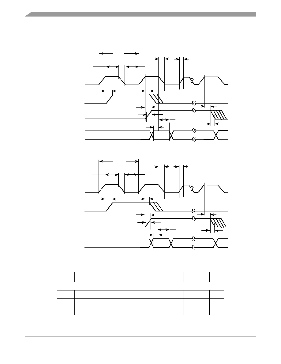
i.MX31/i.MX31L Advance Information, Rev. 1.4
150
Freescale Semiconductor
Preliminary
Electrical Characteristics
4.3.22.4
SSI Receiver Timing with External Clock
Figure 86
depicts the SSI receiver timing with external clock, and
Table 64
lists the timing parameters.
Figure 86. SSI Receiver with External Clock Timing Diagram
Table 64. SSI Receiver with External Clock Timing Parameters
ID
Parameter
Min
Max
Unit
External Clock Operation
SS22
(Tx/Rx) CK clock period
81.4
≠
ns
SS23
(Tx/Rx) CK clock high period
36.0
≠
ns
SS24
(Tx/Rx) CK clock rise time
≠
6.0
ns
SS24
SS34
SS35
SS30
SS28
SS26
SS25
SS23
AD1_TXC
AD1_TXFS (bl)
AD1_TXFS (wl)
AD1_RXD
SS40
SS22
SS32
SS36
SS41
(Input)
(Input)
(Input)
(Input)
SS24
SS34
SS35
SS30
SS28
SS26
SS25
SS23
DAM1_T_CLK
DAM1_T_FS (bl)
DAM1_T_FS (wl)
DAM1_RXD
SS40
SS22
SS32
SS36
SS41
(Input)
(Input)
(Input)
(Input)
Electrical Characteristics
i.MX31/i.MX31L Advance Information, Rev. 1.4
Freescale Semiconductor
151
Preliminary
NOTE
All the timings for the SSI are given for a non-inverted serial clock polarity
(TSCKP/RSCKP = 0) and a non-inverted frame sync (TFSI/RFSI = 0). If the
polarity of the clock and/or the frame sync have been inverted, all the timing
remains valid by inverting the clock signal STCK/SRCK and/or the frame
sync STFS/SRFS shown in the tables and in the figures.
NOTE
All timings are on AUDMUX pads when the SSI is being used for data
transfer.
NOTE
"Tx" and "Rx" refer to the Transmit and Receive sections of the SSI.
NOTE
For internal Frame Sync operation using external clock, the FS timing will
be same as that of Tx Data, for example, during the AC97 mode of
operation.
4.3.23
USB Electrical Specifications
This section describes the electrical information of the USBOTG port. The OTG port supports both serial
and parallel interfaces.
The high speed (HS) interface is supported via the ULPI (Ultra Low Pin Count Interface).
Figure 87
depicts the USB ULPI timing diagram, and
Table 65
lists the timing parameters.
SS25
(Tx/Rx) CK clock low period
36.0
≠
ns
SS26
(Tx/Rx) CK clock fall time
≠
6.0
ns
SS28
(Rx) CK high to FS (bl) high
≠10.0
15.0
ns
SS30
(Rx) CK high to FS (bl) low
10.0
≠
ns
SS32
(Rx) CK high to FS (wl) high
≠10.0
15.0
ns
SS34
(Rx) CK high to FS (wl) low
10.0
≠
ns
SS35
(Tx/Rx) External FS rise time
≠
6.0
ns
SS36
(Tx/Rx) External FS fall time
≠
6.0
ns
SS40
SRXD setup time before (Rx) CK low
10.0
≠
ns
SS41
SRXD hold time after (Rx) CK low
2.0
≠
ns
Table 64. SSI Receiver with External Clock Timing Parameters (continued)
ID
Parameter
Min
Max
Unit
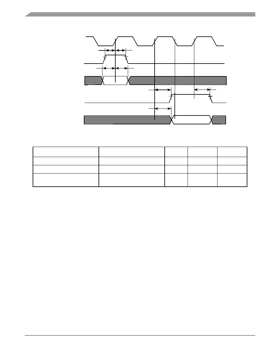
i.MX31/i.MX31L Advance Information, Rev. 1.4
152
Freescale Semiconductor
Preliminary
Package Information and Pinout
Figure 87. USB ULPI Interface Timing Diagram
5
Package Information and Pinout
This section includes the following:
∑
Pin/contact assignment information--usually in the form of a pin-out or contact connection
diagram--for every applicable package, unless this information appears in
Section 3, "Signal
Descriptions."
NOTE:
Either pin or contact is used throughout the data sheet, as appropriate for the
device.
∑
Mechanical package drawing for every applicable package
∑
Ordering information (if this information isn't included on page 1).
The i.MX31 and i.MX31L devices are available in the following package:
∑
457 MAPBGA 14 x 14 mm 0.5 mm pitch package for production (
Figure 88
).
Table 65. USB ULPI Interface Timing Specification
1
1
Timing parameters are given as viewed by transceiver side.
Parameter Symbol
Min
Max
Units
Setup time (control in, 8-bit data in)
T
SC
, T
SD
6.0
ns
Hold time (control in, 8-bit data in)
T
HC
, T
HD
0.0
ns
Output delay (control out, 8-bit data
out)
T
DC
, T
DD
9.0
ns
Clock
Control out (stp)
Data out
Control in (dir, nxt)
Data in
T
DD
T
DC
T
DC
T
SC
T
SD
T
HD
T
HC

Package Information and Pinout
i.MX31/i.MX31L Advance Information, Rev. 1.4
Freescale Semiconductor
153
Preliminary
5.1
MAPBGA Production Package 457 14 x 14 mm, 0.5 P
See
Figure 88
for package drawings and dimensions of the production package.
i.MX31/i.MX31L Advance Information, Rev. 1.4
154
Freescale Semiconductor
Preliminary
Package Information and Pinout
5.1.1
Production Package Outline Drawing
Figure 88. Production Package: Mechanical Drawing

Package Information and Pinout
i.MX31/i.MX31L Advance Information, Rev. 1.4
Freescale Semiconductor
155
Preliminary
5.1.2
MAPBGA Pinout for Production Package
Figure 89
shows the i.MX31/i.MX31L ball map of pad locations.
i.MX31/i.MX31L A
d
v
a
nce
In
f
o
rmat
ion
, Re
v
. 1.4
156
F
r
e
e
scale
Semico
nductor
Preli
m
i
nar
y
Pack
age
Informa
tion and Pinout
Figure 89. i.MX31/i.MX31L Ball Map
1
2
3
4
5
6
7
8
9
10
11
12
13
14
15
16
17
18
19
20
21
22
23
24
25
26
A
GND
GND
SFS5
CSPI2
_MISO
CSPI2_
SS2
USBOT
G_DAT
A7
USBOT
G_DAT
A3
USBOT
G_NXT
USB_B
YP
RXD1
DSR_D
CE1
DSR_D
TE1
RXD2
CE_CO
NTROL
KEY_R
OW3
KEY_R
OW7
KEY_C
OL3
KEY_C
OL7
TDO
SJC_M
OD
SVEN0
CAPTU
RE
GPIO1_
6
WATCH
DOG_R
ST
GND
GND
A
B
GND
GND
STXD4 SRXD
5
CSPI2_
SS0
CSPI2_
SPI_R
DY
USBOT
G_DAT
A5
USBOT
G_DAT
A1
USBOT
G_DIR
USB_P
WR
CTS1
DCD_D
CE1
DCD_D
TE1
RTS2
KEY_R
OW1
KEY_R
OW5
KEY_C
OL1
KEY_C
OL5
TCK
TRSTB SRX0
SCLK0
GPIO1_
1
GPIO1_
5
GND
GND
B
C
GND
GND
SRXD4 SCK4 STXD5 CSPI2_
SS1
CSPI2_
SCLK
USBOT
G_DAT
A4
USBOT
G_STP
USB_O
C
DTR_D
CE1
DTR_D
TE1
TXD2
KEY_R
OW2
KEY_C
OL0
KEY_C
OL4
RTCK
DE
SRST0 GPIO1
_2
BOOT_
MODE1
BOOT_
MODE3
CLKO
GND
GND
GND
C
D
GND
CSPI3_
MOSI
SCK5
BOOT_
MODE2
GND
BOOT_
MODE4
D
E
CSPI3_
SCLK
ATA_DI
OR
CSPI2_
MOSI
NVCC5
GND
GND
DVFS0
POWER
_FAIL
E
F
ATA_D
MACK
ATA_C
S1
SFS4
NVCC5 BATT_
LINE
USBOT
G_DAT
A6
USBOT
G_DAT
A0
TXD1
RI_DC
E1
DTR_D
CE2
KEY_R
OW0
KEY_R
OW6
KEY_C
OL6
TDI
STX0
GPIO1
_0
GPIO1
_4
BOOT_
MODE
0
GND
CKIH
GPIO1_
3
VSTBY
F
G
PWMO PC_R
W
CSPI3_
MISO
CSPI3_
SPI_R
DY
NVCC5
USBOT
G_DAT
A2
USBOT
G_CLK
RTS1
RI_DT
E1
CTS2
KEY_R
OW4
KEY_C
OL2
TMS
SIMPD
0
COMP
ARE
NVCC1
NVCC1
DVFS1
VPG0
CLKSS
G
H
PC_RS
T
PC_BV
D1
ATA_R
ESET
ATA_DI
OW
CKIL
POR
I2C_DA
T
GPIO3_
1
H
J
PC_VS
1
PC_RE
ADY
IOIS16
ATA_C
S0
PC_PO
E
QVCC1 QVCC1 NVCC8 NVCC8 QVCC
NVCC6 NVCC6 NVCC9
VPG1
RESET_
IN
I2C_CL
K
CSI_VS
YNC
CSI_PIX
CLK
J
K
PC_CD
2
SD1_D
ATA3
PC_P
WRON
PC_BV
D2
PC_VS
2
QVCC1
NVCC6
NVCC1
CSI_H
SYNC
GPIO3_
0
CSI_MC
LK
CSI_D5 CSI_D7
K
L
SD1_D
ATA1
SD1_C
MD
SD1_D
ATA2
PC_WA
IT
PC_CD
1
NVCC3
QVCC1 GND
QVCC
QVCC
QVCC
QVCC
NVCC4 NVCC4 CSI_D8 CSI_D4
CSI_D6 CSI_D9 CSI_D1
1
L
M
USBH2
_DATA0
USBH2
_STP
USBH2
_DATA1
SD1_D
ATA0
SD1_C
LK
NVCC3
GND
GND
GND
GND
GND
GND
QVCC
CSI_D1
4
CSI_D1
2
CSI_D1
0
CSI_D1
3
CSI_D1
5
M
N
USBH2
_CLK
CSPI1_
SCLK
CSPI1_
SPI_R
DY
USBH2
_NXT
USBH2
_DIR
QVCC4
NVCC3 GND
GND
GND
GND
GND
NVCC7
SD_D_I FPSHIF
T
VSYNC
0
HSYNC DRDY0
N
P
CSPI1_
SS1
CSPI1_
MOSI
CSPI1_
SS0
CSPI1_
SS2
CSPI1_
MISO
NVCC1
0
NVCC1
0
GND
GND
GND
GND
GND
NVCC7
READ
LCS1
SD_D_
CLK
SD_D_I
O
LCS0
P
R
STXD3 SCK3
SRXD3
SFS3
SRXD6
QVCC4
NVCC1
0
GND
GND
GND
GND
GND
NVCC7
D3_CL
S
PAR_RS
CONTR
AST
WRITE
VSYNC
3
R
T
STXD6 SCK6
SFS6
NFCE
NFWE
QVCC4
NVCC1
0
GND
GND
SGND
MGND UGND
NVCC7
LD4
LD2
LD0
SER_R
S
D3_REV
T
U
NFRB
NFWP NFCLE
D15
D11
QVCC4
QVCC
TTM_P
AD
LD8
LD6
D3_SPL LD1
U
V
NFALE NFRE
D13
D9
D5
QVCC
QVCC
QVCC
QVCC
SVCC
MVCC UVCC
GND
LD17
LD13
LD10
LD3
LD5
V
W D14
D12
D7
D3
NVCC2
2
EB0
LD15
LD7
LD9
W
Y
D10
D8
D1
IOQVD
D
NVCC2
2
NVCC2
2
NVCC2
2
NVCC2
2
NVCC2
2
NVCC2
2
NVCC2
2
NVCC2
1
NVCC2
1
NVCC2
1
NVCC2 NVCC2 NVCC2 NVCC2 M_GRA
NT
EB1
LD11
LD12
Y
AA D6
D4
A4
NVCC2
2
SD31
SD28
SD27
SD23
SD21
SD18
SD16
SD13
SD9
SD7
SD5
SD3
SD2
DQM2
SDCLK
FVCC
LD14
LD16
AA
AB D2
D0
A6
A2
RW
FGND
OE
BCLK
AB
AC MA10
GND
A11
FUSE_V
DD
M_REQ
UEST
GND
AC
AD GND
GND
A12
A13
A8
A0
SDBA0 SDQS3 SD29
SD25
SDQS2 SD17
SD15
SD12
SD8
SDQS0 SD4
SD0
DQM1
CAS
SDCKE
0
CS3
ECB
GND
GND
GND
AD
AE GND
GND
A7
A3
SDBA1 SD30
SD26
SD24
SD22
SD20
SD19
SDQS1 SD14
SD11
SD10
SD6
SD1
DQM3
DQM0
SDCLK CS2
LBA
CS0
GND
GND
GND
AE
AF GND
GND
A9
A5
A1
A25
A24
A23
A22
A21
A20
A19
A18
A17
A16
A15
A14
A10
RAS
SDWE SDCKE
1
CS5
CS1
CS4
GND
GND
AF
1
2
3
4
5
6
7
8
9
10
11
12
13
14
15
16
17
18
19
20
21
22
23
24
25
26
Package Information and Pinout
i.MX31/i.MX31L Advance Information, Rev. 1.4
Freescale Semiconductor
157
Preliminary
Figure 66
shows the signal color and signal name legend.
Table 67
shows the device pin list, sorted by signal identification, excluding pad locations for ground and
power supply voltages.
Table 66. Signal Color/Name Legend
Color
Name
None
Signal name as listed
GND
NVCC1
NVCC2
NVCC3
NVCC4
NVCC5
NVCC6
NVCC7
NVCC8
NVCC9
NVCC10
NVCC21
NVCC22
QVCC
QVCC1
QVCC4
Table 67. i.MX31/i.MX31L 14 x 14 BGA (457 Signal ID by Pad Grid Location)
Signal ID
Pad Location
A0
AD6
A1
AF5
A10
AF18
A11
AC3
A12
AD3
A13
AD4
A14
AF17
A15
AF16
i.MX31/i.MX31L Advance Information, Rev. 1.4
158
Freescale Semiconductor
Preliminary
Package Information and Pinout
A16
AF15
A17
AF14
A18
AF13
A19
AF12
A2
AB5
A20
AF11
A21
AF10
A22
AF9
A23
AF8
A24
AF7
A25
AF6
A3
AE4
A4
AA3
A5
AF4
A6
AB3
A7
AE3
A8
AD5
A9
AF3
ATA_CS0
J6
ATA_CS1
F2
ATA_DIOR
E2
ATA_DIOW
H6
ATA_DMACK
F1
ATA_RESET
H3
BATT_LINE
F7
BCLK
AB26
BOOT_MODE0
F20
BOOT_MODE1
C21
BOOT_MODE2
D24
BOOT_MODE3
C22
BOOT_MODE4
D26
CAPTURE
A22
CAS
AD20
CE_CONTROL
A14
CKIH
F24
CKIL
H21
CLKO
C23
Table 67. i.MX31/i.MX31L 14 x 14 BGA (457 Signal ID by Pad Grid Location) (continued)
Signal ID
Pad Location
Package Information and Pinout
i.MX31/i.MX31L Advance Information, Rev. 1.4
Freescale Semiconductor
159
Preliminary
CLKSS
G26
COMPARE
G18
CONTRAST
R24
CS0
AE23
CS1
AF23
CS2
AE21
CS3
AD22
CS4
AF24
CS5
AF22
CSI_D10
M24
CSI_D11
L26
CSI_D12
M21
CSI_D13
M25
CSI_D14
M20
CSI_D15
M26
CSI_D4
L21
CSI_D5
K25
CSI_D6
L24
CSI_D7
K26
CSI_D8
L20
CSI_D9
L25
CSI_HSYNC
K20
CSI_MCLK
K24
CSI_PIXCLK
J26
CSI_VSYNC
J25
CSPI1_MISO
P7
CSPI1_MOSI
P2
CSPI1_SCLK
N2
CSPI1_SPI_RDY
N3
CSPI1_SS0
P3
CSPI1_SS1
P1
CSPI1_SS2
P6
CSPI2_MISO
A4
CSPI2_MOSI
E3
CSPI2_SCLK
C7
CSPI2_SPI_RDY
B6
CSPI2_SS0
B5
Table 67. i.MX31/i.MX31L 14 x 14 BGA (457 Signal ID by Pad Grid Location) (continued)
Signal ID
Pad Location

i.MX31/i.MX31L Advance Information, Rev. 1.4
160
Freescale Semiconductor
Preliminary
Package Information and Pinout
CSPI2_SS1
C6
CSPI2_SS2
A5
CSPI3_MISO
G3
CSPI3_MOSI
D2
CSPI3_SCLK
E1
CSPI3_SPI_RDY
G6
CTS1
B11
CTS2
G13
D0
AB2
D1
Y3
D10
Y1
D11
U7
D12
W2
D13
V3
D14
W1
D15
U6
D2
AB1
D3
W6
D3_CLS
R20
D3_REV
T26
D3_SPL
U25
D4
AA2
D5
V7
D6
AA1
D7
W3
D8
Y2
D9
V6
DCD_DCE1
B12
DCD_DTE1
B13
DE
C18
DQM0
AE19
DQM1
AD19
DQM2
AA20
DQM3
AE18
DRDY0
N26
DSR_DCE1
A11
DSR_DTE1
A12
Table 67. i.MX31/i.MX31L 14 x 14 BGA (457 Signal ID by Pad Grid Location) (continued)
Signal ID
Pad Location

Package Information and Pinout
i.MX31/i.MX31L Advance Information, Rev. 1.4
Freescale Semiconductor
161
Preliminary
DTR_DCE1
C11
DTR_DCE2
F12
DTR_DTE1
C12
DVFS0
E25
DVFS1
G24
EB0
W21
EB1
Y24
ECB
AD23
FGND
AB24
FPSHIFT
N21
FUSE_VDD
AC24
FVCC
AA24
GPIO1_0
F18
GPIO1_1
B23
GPIO1_2
C20
GPIO1_3
F25
GPIO1_4
F19
GPIO1_5
B24
GPIO1_6
A23
GPIO3_0
K21
GPIO3_1
H26
HSYNC
N25
I2C_CLK
J24
I2C_DAT
H25
IOIS16
J3
IOQVDD
Y6
KEY_COL0
C15
KEY_COL1
B17
KEY_COL2
G15
KEY_COL3
A17
KEY_COL4
C16
KEY_COL5
B18
KEY_COL6
F15
KEY_COL7
A18
KEY_ROW0
F13
KEY_ROW1
B15
KEY_ROW2
C14
Table 67. i.MX31/i.MX31L 14 x 14 BGA (457 Signal ID by Pad Grid Location) (continued)
Signal ID
Pad Location
i.MX31/i.MX31L Advance Information, Rev. 1.4
162
Freescale Semiconductor
Preliminary
Package Information and Pinout
KEY_ROW3
A15
KEY_ROW4
G14
KEY_ROW5
B16
KEY_ROW6
F14
KEY_ROW7
A16
LBA
AE22
LCS0
P26
LCS1
P21
LD0
T24
LD1
U26
LD10
V24
LD11
Y25
LD12
Y26
LD13
V21
LD14
AA25
LD15
W24
LD16
AA26
LD17
V20
LD2
T21
LD3
V25
LD4
T20
LD5
V26
LD6
U24
LD7
W25
LD8
U21
LD9
W26
M_GRANT
Y21
M_REQUEST
AC25
MA10
AC1
MGND
T15
MVCC
V15
NFALE
V1
NFCE
T6
NFCLE
U3
NFRB
U1
NFRE
V2
NFWE
T7
Table 67. i.MX31/i.MX31L 14 x 14 BGA (457 Signal ID by Pad Grid Location) (continued)
Signal ID
Pad Location
Package Information and Pinout
i.MX31/i.MX31L Advance Information, Rev. 1.4
Freescale Semiconductor
163
Preliminary
NFWP
U2
NVCC9
J17
OE
AB25
PAR_RS
R21
PC_BVD1
H2
PC_BVD2
K6
PC_CD1
L7
PC_CD2
K1
PC_POE
J7
PC_PWRON
K3
PC_READY
J2
PC_RST
H1
PC_RW
G2
PC_VS1
J1
PC_VS2
K7
PC_WAIT
L6
POR
H24
POWER_FAIL
E26
PWMO
G1
RAS
AF19
READ
P20
RESET_IN
J21
RI_DCE1
F11
RI_DTE1
G12
RTCK
C17
RTS1
G11
RTS2
B14
RW
AB22
RXD1
A10
RXD2
A13
SCK3
R2
SCK4
C4
SCK5
D3
SCK6
T2
SCLK0
B22
SD_D_CLK
P24
SD_D_I
N20
Table 67. i.MX31/i.MX31L 14 x 14 BGA (457 Signal ID by Pad Grid Location) (continued)
Signal ID
Pad Location
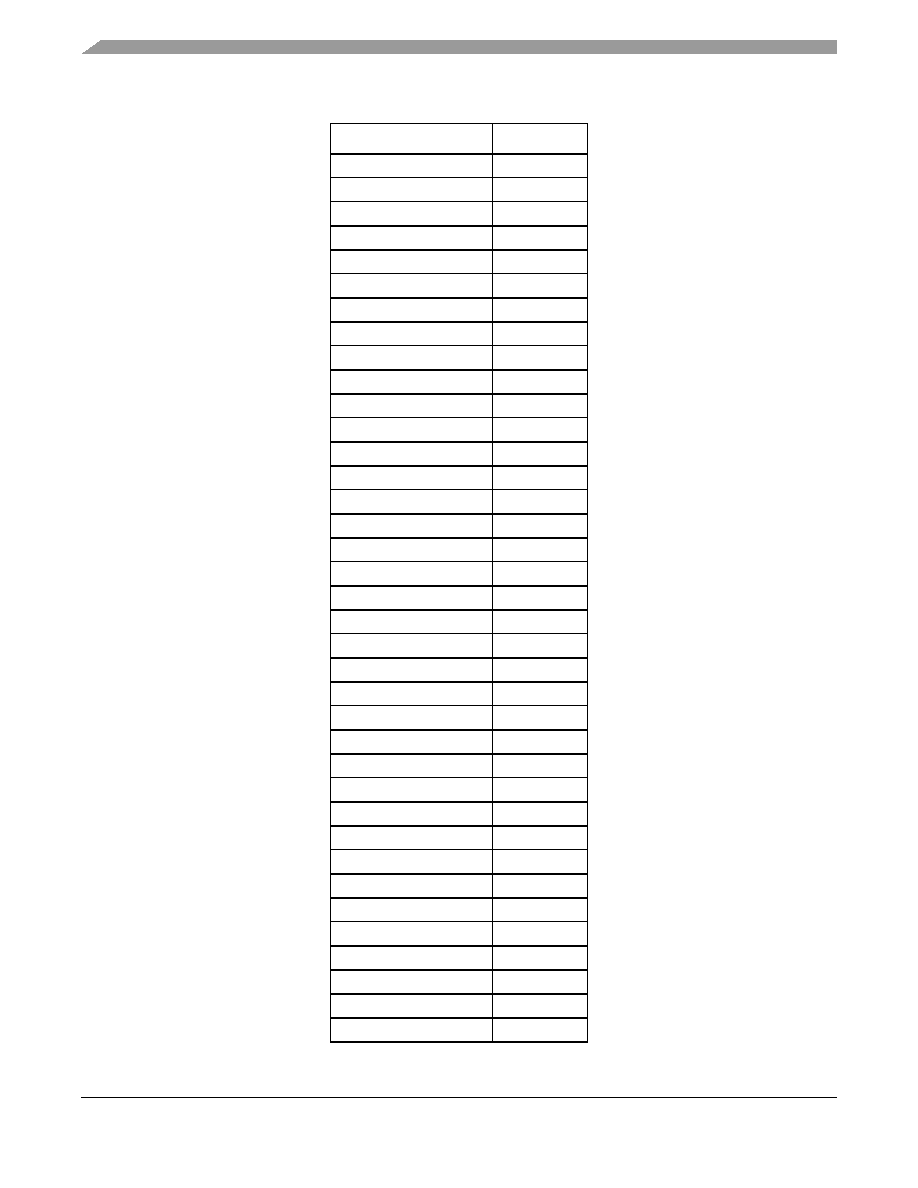
i.MX31/i.MX31L Advance Information, Rev. 1.4
164
Freescale Semiconductor
Preliminary
Package Information and Pinout
SD_D_IO
P25
SD0
AD18
SD1
AE17
SD1_CLK
M7
SD1_CMD
L2
SD1_DATA0
M6
SD1_DATA1
L1
SD1_DATA2
L3
SD1_DATA3
K2
SD10
AE15
SD11
AE14
SD12
AD14
SD13
AA14
SD14
AE13
SD15
AD13
SD16
AA13
SD17
AD12
SD18
AA12
SD19
AE11
SD2
AA19
SD20
AE10
SD21
AA11
SD22
AE9
SD23
AA10
SD24
AE8
SD25
AD10
SD26
AE7
SD27
AA9
SD28
AA8
SD29
AD9
SD3
AA18
SD30
AE6
SD31
AA7
SD4
AD17
SD5
AA17
SD6
AE16
SD7
AA16
Table 67. i.MX31/i.MX31L 14 x 14 BGA (457 Signal ID by Pad Grid Location) (continued)
Signal ID
Pad Location
Package Information and Pinout
i.MX31/i.MX31L Advance Information, Rev. 1.4
Freescale Semiconductor
165
Preliminary
SD8
AD15
SD9
AA15
SDBA0
AD7
SDBA1
AE5
SDCKE0
AD21
SDCKE1
AF21
SDCLK
AA21
SDCLK
AE20
SDQS0
AD16
SDQS1
AE12
SDQS2
AD11
SDQS3
AD8
SDWE
AF20
SER_RS
T25
SFS3
R6
SFS4
F3
SFS5
A3
SFS6
T3
SGND
T14
SIMPD0
G17
SJC_MOD
A20
SRST0
C19
SRX0
B21
SRXD3
R3
SRXD4
C3
SRXD5
B4
SRXD6
R7
STX0
F17
STXD3
R1
STXD4
B3
STXD5
C5
STXD6
T1
SVCC
V14
SVEN0
A21
TCK
B19
TDI
F16
TDO
A19
Table 67. i.MX31/i.MX31L 14 x 14 BGA (457 Signal ID by Pad Grid Location) (continued)
Signal ID
Pad Location
i.MX31/i.MX31L Advance Information, Rev. 1.4
166
Freescale Semiconductor
Preliminary
Package Information and Pinout
TMS
G16
TRSTB
B20
TTM_PAD
U20
TXD1
F10
TXD2
C13
UVCC
V16
USB_BYP
A9
USB_OC
C10
USB_PWR
B10
USBH2_CLK
N1
USBH2_DATA0
M1
USBH2_DATA1
M3
USBH2_DIR
N7
USBH2_NXT
N6
USBH2_STP
M2
USBOTG_CLK
G10
USBOTG_DATA0
F9
USBOTG_DATA1
B8
USBOTG_DATA2
G9
USBOTG_DATA3
A7
USBOTG_DATA4
C8
USBOTG_DATA5
B7
USBOTG_DATA6
F8
USBOTG_DATA7
A6
USBOTG_DIR
B9
USBOTG_NXT
A8
USBOTG_STP
C9
UGND
T16
VPG0
G25
VPG1
J20
VSTBY
F26
VSYNC0
N24
VSYNC3
R26
WATCHDOG_RST
A24
WRITE
R25
Table 67. i.MX31/i.MX31L 14 x 14 BGA (457 Signal ID by Pad Grid Location) (continued)
Signal ID
Pad Location

Product Documentation
i.MX31/i.MX31L Advance Information, Rev. 1.4
Freescale Semiconductor
167
Preliminary
6
Product Documentation
This Data Sheet is labeled as a particular type: Product Preview, Advance Information, or Technical Data.
Definitions of these types are available at: http://www.freescale.com.
6.1
Revision History
Table 68
summarizes revisions to this document since the release
of Rev. 1.2.
Table 68. Revision History
Location
Revision
Table 9, "DC Recommended Operating
Conditions," on page 61
Core Supply voltage--changed minimum voltage FROM 1.2 V TO 1.22 V.
Table 10, "Voltage versus Core Frequency,"
on page 62
∑ Min (V) for 1st row--changed value FROM 1.2 V to 1.22 V.
∑ Added footnotes.
Table 13, "Power Consumption (Typical
Values)," on page 64
Updated entire table.
Section 4.3.8, "DPLL Electrical
Specifications
" starting
on page 82
Updated DPLL section for content. Replaced HI/LO with content about external
clock source (CKIH) and FPM (Frequency Pre-Multiplier).
Table 34, "DDR/SDR SDRAM Read Cycle
Timing Parameters," on page 94
,
Table 35,
"SDR SDRAM Write Timing Parameters," on
page 96
∑ Changed SD4, SD6 min values FROM 1.8 V TO 2.0 V.
∑ Changed SD13 min value FROM 2.4 V TO 2.0 V.
Section 4.3.10, "ETM Electrical
Specifications
"
on page 100
,
Table 41, "ETM
Trace Data Timing Parameters," on page
101
.
At ETM Trace Data Timing Parameters table: Changed Ts Setup value FROM 3
TO 2, changed Th Hold value FROM 2 TO 1.
Table 60, "SJC Timing Parameters," on
page 143
∑ SJ1 row--Removed "in Crystal mode", changed min value FROM 45.0 ns TO
100.0 ns.
∑ Changed SJ2 min value FROM 22.5 ns TO 40.0 ns.
∑ Changed SJ4 min value FROM 5.0 ns TO 10.0 ns.
∑ Changed SJ5 min value FROM 24.0 ns TO 50.0 ns.
∑ Changed SJ8 min value FROM 5.0 ns TO 10.0 ns.
∑ Changed SJ9 min value FROM 25.0 ns TO 50.0 ns.
Section 4.3.2, "AC Electrical
Characteristics
" starting
on page 68
Updated section for figure, table values.
Section 2.1.1, "Performance
"
on page 4
Updated section.
Table 11, "Interface Frequency," on page 62
Updated.
Section 4.3.23, "USB Electrical
Specifications
"
on page 151
Revised section; added ULPI information.
Figure 89, "i.MX31/i.MX31L Ball Map," on
page 156
Revised for color, grid # ID.

i.MX31/i.MX31L Advance Information, Rev. 1.4
168
Freescale Semiconductor
Preliminary
Product Documentation
Table 23, "ATA Timing Parameters," on page
72
∑ Inserted the following values:
∑ ti_ds, 11 ns
∑ ti_dh, 6 ns
∑ tco, 15 ns
∑ tsu, 19 ns
∑ tsui, 9 ns
∑ thi, 5 ns
∑ Changed tskew1 value FROM 20 ns TO 7 ns.
Table 29, "CSPI Interface Timing
Parameters," on page 81
Changed CS4, CS5, CS6 min values FROM 30 ns TO 25 ns.
Table 33, "WEIM Bus Timing Parameters,"
on page 89
Updated entire table.
Table 49, "Synchronous Display Interface
Timing Parameters--Access Level," on
page 110
Changed IP18 min value FROM Tdicd-1.5 TO Tdicd-3.5.
Changed IP19 min value FROM Tdicp-Tdicd-1.5 TO Tdicp-Tdicd-3.5.
Changed IP20 min value FROM Tdicd-1.5 TO Tdicd-3.5.
Above
Figure 30, "Asynchronous Memory
Timing Diagram for Read
Access--WSC=1," on page 91
Changed pad voltage FROM 1.7 V TO 1.75 V.
Section 4.1, "i.MX31 and i.MX31L
Chip-Level Conditions
" starting
on page 60
∑
Table 9, "DC Recommended Operating Conditions," on page 61
--changed
Core Supply Voltage row max voltage FROM 1.6 V to 1.65 V, footnote value
FROM 1.6 V TO 1.65 V (2 plcs).
∑
Table 10, "Voltage versus Core Frequency," on page 62
--changed both max
values FROM 1.6 V TO 1.65 V; PMIC value in footnote FROM 1.575 V to 1.6 V.
∑
Table 12, "DC Absolute Maximum Operating Conditions," on page
63
--changed max value FROM 1.6 V to 1.65 V.
Section 4.3.9.3, "SDRAM (DDR and SDR)
Memory Controller
" starting
on page 93
Removed duplicate notes about pad voltages and signal values.
Figure 89, "i.MX31/i.MX31L Ball Map," on
page 156
Corrected pad locations for area of rows E through N, columns 4 through 26.
Table 68. Revision History (continued)
Location
Revision

Product Documentation
i.MX31/i.MX31L Advance Information, Rev. 1.4
Freescale Semiconductor
169
Preliminary

Document Number: MCIMX31
Rev. 1.4
04/2006
Preliminary
How to Reach Us:
Home Page:
www.freescale.com
E-mail:
support@freescale.com
USA/Europe or Locations Not Listed:
Freescale Semiconductor
Technical Information Center, CH370
1300 N. Alma School Road
Chandler, Arizona 85224
+1-800-521-6274 or +1-480-768-2130
support@freescale.com
Europe, Middle East, and Africa:
Freescale Halbleiter Deutschland GmbH
Technical Information Center
Schatzbogen 7
81829 Muenchen, Germany
+44 1296 380 456 (English)
+46 8 52200080 (English)
+49 89 92103 559 (German)
+33 1 69 35 48 48 (French)
support@freescale.com
Japan:
Freescale Semiconductor Japan Ltd.
Headquarters
ARCO Tower 15F
1-8-1, Shimo-Meguro, Meguro-ku,
Tokyo 153-0064, Japan
0120 191014 or +81 3 5437 9125
support.japan@freescale.com
Asia/Pacific:
Freescale Semiconductor Hong Kong Ltd.
Technical Information Center
2 Dai King Street
Tai Po Industrial Estate
Tai Po, N.T., Hong Kong
+800 2666 8080
support.asia@freescale.com
For Literature Requests Only:
Freescale Semiconductor Literature Distribution Center
P.O. Box 5405
Denver, Colorado 80217
1-800-521-6274 or 303-675-2140
Fax: 303-675-2150
LDCForFreescaleSemiconductor@hibbertgroup.com
Information in this document is provided solely to enable system and software implementers to use
Freescale Semiconductor products. There are no express or implied copyright licenses granted
hereunder to design or fabricate any integrated circuits or integrated circuits based on the information
in this document.
Freescale Semiconductor reserves the right to make changes without further notice to any products
herein. Freescale Semiconductor makes no warranty, representation or guarantee regarding the
suitability of its products for any particular purpose, nor does Freescale Semiconductor assume any
liability arising out of the application or use of any product or circuit, and specifically disclaims any
and all liability, including without limitation consequential or incidental damages. "Typical" parameters
that may be provided in Freescale Semiconductor data sheets and/or specifications can and do vary
in different applications and actual performance may vary over time. All operating parameters,
including "Typicals", must be validated for each customer application by customer's technical experts.
Freescale Semiconductor does not convey any license under its patent rights nor the rights of others.
Freescale Semiconductor products are not designed, intended, or authorized for use as components
in systems intended for surgical implant into the body, or other applications intended to support or
sustain life, or for any other application in which the failure of the Freescale Semiconductor product
could create a situation where personal injury or death may occur. Should Buyer purchase or use
Freescale Semiconductor products for any such unintended or unauthorized application, Buyer shall
indemnify and hold Freescale Semiconductor and its officers, employees, subsidiaries, affiliates, and
distributors harmless against all claims, costs, damages, and expenses, and reasonable attorney
fees arising out of, directly or indirectly, any claim of personal injury or death associated with such
unintended or unauthorized use, even if such claim alleges that Freescale Semiconductor was
negligent regarding the design or manufacture of the part.
FreescaleTM and the Freescale logo are trademarks of Freescale Semiconductor, Inc. ARM, ARM
Thumb, Jazelle, and the ARM Powered logo are registered trademarks of ARM Limited.
ARM1136JF-S, ARM11, Embedded Trace Kit, Embedded Trace Macrocell, ETM, Embedded Trace
Buffer, and ETB are trademarks of ARM Limited. All other product or service names are the property
of their respective owners. Java and all other Java-based marks are trademarks or registered
trademarks of Sun Microsystems, Inc. in the U.S. and other countries. France Telecom ≠ TDF ≠
Groupe des ecoles des telecommunications Turbo codes patents license.
© Freescale Semiconductor, Inc. 2005, 2006. All rights reserved.