MHV5IC1810NR2
1
RF Device Data
Freescale Semiconductor
RF LDMOS Wideband Integrated
Power Amplifier
The MHV5IC1810N wideband integrated circuit is designed with on -chip
matching that makes it usable from 1805 to 1990 MHz. This multi -stage
structure is rated for 24 to 32 Volt operation and covers all typical cellular base
station modulation formats.
Final Application
∑ Typical Two-Tone Performance: V
DD
= 28 Volts, I
DQ1
= 120 mA, I
DQ2
=
90 mA, P
out
= 5 Watts Avg., Full Frequency Band (1805-1880 MHz or
1930 -1990 MHz)
Power Gain -- 29 dB
Power Added Efficiency -- 29%
IMD -- -34 dBc
Driver Application
∑ Typical GSM EDGE Performance: V
DD
= 28 Volts, I
DQ1
= 105 mA, I
DQ2
=
95 mA, P
out
= 35 dBm, Full Frequency Band (1805-1880 MHz or
1930 -1990 MHz)
Power Gain -- 29 dB
Spectral Regrowth @ 400 kHz Offset = -67 dBc
Spectral Regrowth @ 600 kHz Offset = -76 dBc
EVM -- 1.1% rms
∑ Capable of Handling 3:1 VSWR, @ 28 Vdc, 1990 MHz, 10 Watts CW
Output Power
∑ Stable into a 3:1 VSWR. All Spurs Below -60 dBc @ 100 mW to 10 W CW
P
out
.
Features
∑ Characterized with Series Equivalent Large-Signal Impedance Parameters
and Common Source Scattering Parameters
∑ On-Chip Matching (50 Ohm Input, >5 Ohm Output)
∑ Integrated Quiescent Current Temperature Compensation
with Enable/Disable Function
∑ On-Chip Current Mirror g
m
Reference FET for Self Biasing Application
(1)
∑ Integrated ESD Protection
∑ RoHS Compliant
∑ In Tape and Reel. R2 Suffix = 1500 Units per 16 mm, 13 inch Reel.
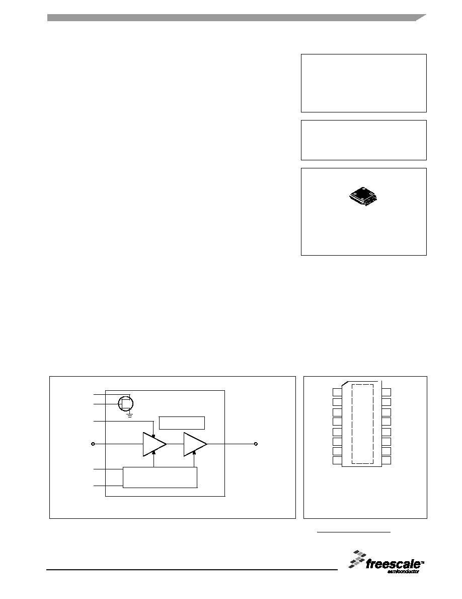
16
15
14
13
12
11
10
1
2
3
4
5
6
7
8
(Top View)
9
NC
V
DS1
GND
V
GS1
V
GS2
NC
V
DS2
/RF
out
V
DS2
/RF
out
V
DS2
/RF
out
V
DS2
/RF
out
V
DS2
/RF
out
V
DS2
/RF
out
NC
V
GS1
RF
in
V
DS1
V
GS2
RF
in
V
DS2
/RF
out
2 Stage IC
Quiescent Current
Temperature Compensation
V
RD1
V
RG1
V
RD1
V
RG1
Note: Exposed backside flag is source
terminal for transistors.
Figure 1. Functional Block Diagram
Figure 2. Pin Connections
1. Refer to AN1987, Quiescent Current Control for the RF Integrated Circuit Device Family. Go to http://www.freescale.com/rf.
Select Documentation/Application Notes - AN1987.
Document Number: MHV5IC1810N
Rev. 0, 5/2006
Freescale Semiconductor
Technical Data
MHV5IC1810NR2
1805 -1990 MHz, 5 W AVG., 28 V
GSM/GSM EDGE
RF LDMOS WIDEBAND
INTEGRATED POWER AMPLIFIER
CASE 978-03
PFP -16
PLASTIC
16
1
© Freescale Semiconductor, Inc., 2006. All rights reserved.
2
RF Device Data
Freescale Semiconductor
MHV5IC1810NR2
Table 1. Maximum Ratings
Rating
Symbol
Value
Unit
Drain-Source Voltage
V
DSS
-0.5, +65
Vdc
Gate-Source Voltage
V
GS
-0.5, +12
Vdc
Storage Temperature Range
T
stg
-65 to +150
∞C
Operating Junction Temperature
T
J
150
∞C
Input Power
P
in
12
dBm
Table 2. Thermal Characteristics
Characteristic
Symbol
Value
(1)
Unit
Thermal Resistance, Junction to Case
Final Application
Stage 1, 28 Vdc, I
DQ1
= 120 mA
(P
out
= 10 W CW)
Stage 2, 28 Vdc, I
DQ2
= 90 mA
Driver Application
Stage 1, 28 Vdc, I
DQ1
= 120 mA
(P
out
= 2.25 W CW)
Stage 2, 28 Vdc, I
DQ2
= 90 mA
R
JC
9.2
3.3
10
3.5
∞C/W
Table 3. ESD Protection Characteristics
Test Methodology
Class
Human Body Model (per JESD22-A114)
0 (Minimum)
Machine Model (per EIA/JESD22-A115)
A (Minimum)
Charge Device Model (per JESD22-C101)
III (Minimum)
Table 4. Moisture Sensitivity Level
Test Methodology
Rating
Package Peak Temperature
Unit
Per JESD 22-A113, IPC/JEDEC J-STD-020
3
260
∞C
Table 5. Electrical Characteristics
(T
C
= 25∞C unless otherwise noted)
Characteristic
Symbol
Min
Typ
Max
Unit
Functional Tests (In Freescale Wideband 1930-1990 MHz Test Fixture, 50 ohm system) V
DD
= 28 Vdc, I
DQ1
= 120 mA, I
DQ2
= 90 mA,
P
out
= 5 W Avg., f1 = 1990 MHz, f2 = 1990.1 MHz, Two-Tone Test
Power Gain
G
ps
26.5
29
--
dB
Power Added Efficiency
PAE
25
29
--
%
Intermodulation Distortion
IMD
--
-34
-27
dBc
Input Return Loss
IRL
--
-10
dB
Typical
Two-Tone Performances (In Freescale Test Fixture, 50 hm system) V
DD
= 28 Vdc, I
DQ1
= 120 mA, I
DQ2
= 90 mA, P
out
=
5 W Avg., 1805-1880 MHz
Power Gain
G
ps
--
29
--
dB
Power Added Efficiency
PAE
--
29
--
%
Intermodulation Distortion
IMD
--
-34
--
dBc
Input Return Loss
IRL
--
-15
--
dB
Typical GSM EDGE Performances (In Freescale GSM EDGE Test Fixture, 50 hm system) V
DD
= 28 Vdc, I
DQ1
= 105 mA, I
DQ2
= 95 mA,
P
out
= 3.2 W Avg., 1805-1880 MHz or 1930-1990 MHz EDGE Modulation
Power Gain
G
ps
--
29
--
dB
Error Vector Magnitude
EVM
--
1.1
--
% rms
Spectral Regrowth at 400 kHz Offset
SR1
--
-67
--
dBc
Spectral Regrowth at 600 kHz Offset
SR2
--
-76
--
dBc
1. Refer to AN1955, Thermal Measurement Methodology of RF Power Amplifiers. Go to http://www.freescale.com/rf.
Select Documentation/Application Notes - AN1955.

MHV5IC1810NR2
3
RF Device Data
Freescale Semiconductor
Table 5. Electrical Characteristics -- continued
(T
C
= 25∞C unless otherwise noted) (
continued)
Characteristic
Symbol
Min
Typ
Max
Unit
Typical CW Performances (In Freescale CW Test Fixture, 50 hm system) V
DD
= 28 Vdc, I
DQ1
= 120 mA, I
DQ2
= 90 mA, P
out
=
2.25 W Avg., 1805-1990 MHz
Power Gain
G
ps
--
29
--
dB
Power Added Efficiency
PAE
--
19
--
%
Input Return Loss
IRL
--
-13
--
dB
4
RF Device Data
Freescale Semiconductor
MHV5IC1810NR2
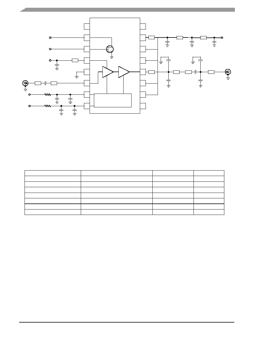
Z7
0.917 x 0.050 Microstrip
Z8
0.304 x 0.050 Microstrip
Z9
0.710 x 0.050 Microstrip
Z10
1.296 x 0.400 Microstrip
PCB
Rogers 4350, 0.020,
r
= 3.50
Z1
0.120 x 0.044 Microstrip
Z2
0.257 x 0.044 Microstrip
Z3
0.103 x 0.170 Microstrip
Z4
0.195 x 0.122 Microstrip
Z5
0.388 x 0.084 Microstrip
Z6
0.273 x 0.044 Microstrip
Figure 3. MHV5IC1810NR2
Test Circuit Schematic -- 1930-1990 MHz
RF
OUTPUT
RF
INPUT
Z10
Z1
Z2
C2
V
GS2
R2
C8
V
GS1
R1
C10
C7
C5
Z8
C9
Z3
Z4
Z5
Z6
C6
C13
C12
NC
NC
V
DS2
V
DS1
V
RG1
V
RD1
NC
Quiescent Current
Temperature Compensation
1
2
3
4
5
6
7
8
16
15
14
13
12
11
10
9
C3
C4
C14
C15
Z9
Z7
C11
Table 6. MHV5IC1810NR2 Test Circuit Component Designations and Values -- 1930-1990 MHz
Part
Description
Part Number
Manufacturer
C2
22 pF 100A Chip Capacitor
100A220GWT
ATC
C3, C4, C5, C6
8.2 pF 100A Chip Capacitors
100A8R2CW
ATC
C7, C8, C9
10 nF Chip Capacitors (0805)
08055C103KAT
AVX
C10, C11
6.8 F Chip Capacitors (1812)
C4532X5R1H685MT
TDK
C12, C13
3.3 pF 100A Chip Capacitors
100A3R3BW
ATC
C14, C15
0.5 pF 100A Chip Capacitors
100A0R5BW
ATC
R1, R2
1 k, 1/8 W Chip Resistors (0805)
MHV5IC1810NR2
5
RF Device Data
Freescale Semiconductor
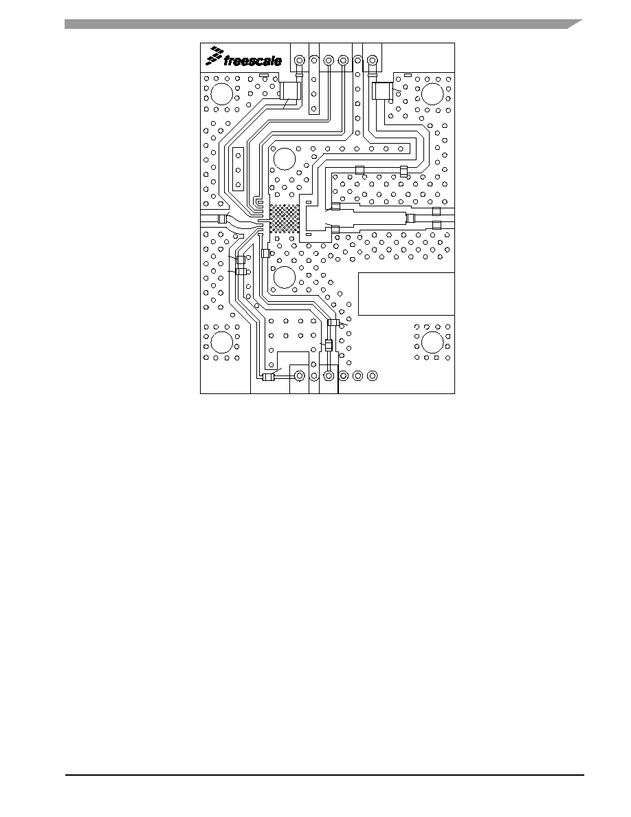
Figure 4. MHV5IC1810NR2 Test Circuit Component Layout -- 1930-1990 MHz
MHV5IC1810N
Rev. 0
C10
V
D1
V
D2
C11
C5
C9
C13
C12
C6
C14
C15
C2
C3
C7
C4
C8
V
GS1
R1
V
GS2
R2